
 Open Access Article
 This Open Access Article is licensed under a Creative Commons Attribution-Non Commercial 3.0 Unported Licence
Large-scale high-numerical-aperture super-oscillatory lens fabricated by direct laser writing lithography
Haibin Ni†
ab,
Guanghui Yuan†c,
Liangdong Suna,
Ning Changa,
Di Zhanga,
Ruipeng Chena,
Liyong Jiangd,
Hongyuan Chene,
Zhongze Gua and
Xiangwei Zhao *a
*a
aState Key Laboratory of Bioelectronics, School of Biological Science and Medical Engineering, National Demonstration Center for Experimental Biomedical Engineering Education, Southeast University, Nanjing 210096, China. E-mail: xwzhao@seu.edu.cn
bJiangsu Key Laboratory of Meteorological Observation and Information Processing, Nanjing University of Information Science and Technology, Nanjing 210044, China
cCentre for Disruptive Photonic Technologies, TPI, SPMS, Nanyang Technological University, Singapore 637371, Singapore
dDepartment of Physics, School of Science, Nanjing University of Science and Technology, Nanjing 210094, China
eState Key Laboratory of Analytical Chemistry for Life Science, School of Chemistry and Chemical Engineering, Nanjing University, Nanjing 210093, China
First published on 4th June 2018
Abstract
In this study, direct laser writing (DLW) lithography is employed to fabricate a large-scale and high-numerical-aperture super-oscillatory lens (SOL), which is capable of achieving a sub-Abbe–Rayleigh diffraction limit focus in the optical far-field region by delicate interference. Large-diameter (600 μm), amplitude-modulated and phase-type SOLs with the smallest annular ring width of 1 μm are fabricated, and they have high quality. The dependence of DLW printing on the fabrication parameters including substrate materials, laser power, and scanning speed is well investigated. A standard procedure to manufacture high-quality binary amplitude SOLs is presented, which avoids direct printing patterns on metal films and reduces the surface roughness dramatically. Random displacements between squares constituting SOLs are discussed, and their influence on the focusing performance is studied by both numerical simulations and experiments. The optical performances of the SOLs fabricated by the DLW method are experimentally characterized, and a needle-like focus with a spot size of 0.42λ and a depth of focus of ∼6 μm are confirmed at a working distance of 100 μm for λ = 633 nm, thus giving an effective numerical aperture as high as 1.19 in air. As a complementary sub-micrometer fabrication method between traditional lithography and nanofabrication method, DLW is proved to be a promising approach to manufacture SOLs, presenting advantages of relatively high speed, low equipment volume, less complexity and sub-micrometer lateral resolution. Such SOLs can be very useful in high resolution bio-imaging on rough surfaces and in the related research fields.
Introduction
Large-scale and high-numerical-aperture planar optical lenses with long working distance, efficient optical throughput and high resolution are highly desirable for applications in mobile devices, camera lenses, and super-resolved imaging. Currently, conventional diffractive optical elements such as zone plates and planar lenses are used, and they utilize properly designed optical masks. An alternative solution can be optical meta-surface lenses, which are assemblies of sub-wavelength-thickness resonant metallic or dielectric optical elements capable of fully controlling local intensity, phase, polarization and spectral responses; these lenses are thus attracting more and more research interest in the nano-photonic fields in the recent years.Among various kinds of planar optical components, the recently developed super-oscillatory lens (SOL) is an interesting candidate, which can meet the requirements of long working distance, high numerical aperture and high resolution. A SOL is a nanostructured mask and on illumination with a coherent light source, it creates a sub-Abbe–Rayleigh diffraction limit focus at a distance in the optical far-field region.1–3 This is related to the fact that band-limited functions are able to locally oscillate arbitrarily faster than their highest Fourier component, and this is a counter-intuitive physical phenomenon now known as super-oscillation.2 By delicate interference of multiple propagating waves, a SOL can also form a needle-like focused beam with extremely long depth of focus in the propagation plane while keeping the sub-diffraction features in the transverse plane. Since their development, SOLs have been used in optical beam lithography,4 super-resolution imaging,1,5 particle acceleration,6 and high-density optical data storage.7,8 Linearly, radially and azimuthally polarized light can be focused to form a needle-like shape with sub-diffraction spot size by diffraction from a phase or amplitude-modulated SOL mask.3,9–16 Achromatic SOLs in the visible range were also proposed recently.1,17 Furthermore, visible-range reconfigurable bi-chromatic and multi-focus SOLs and Fresnel zone plates have also been demonstrated.18 According to the genetic algorithm (GA) or Particle Swarm Optimization (PSO) algorithm,7,14,17,19 the parameters of SOLs can be flexibly tuned by adjusting annular ring numbers and width depending on specific applications.
In the aspect of fabrication, although it is now possible to design efficient wavefront-shaping meta-surfaces with performance comparable to that of the state-of-the-art commercial optical components,20,21 the meta-surface components mostly suffer from constrained fabrication throughput abilities as they generally need line resolution in tens of nanometres, which can now only be achieved by the focused ion beam (FIB) or electron beam lithography (EBL) methods. These two commonly used nanofabrication methods have succeeded in achieving sub-10 nm resolution, but they require expensive facilities, long fabrication time and high vacuum environment, which limits the use of some materials, such as hydrogels, as substrates. Alternative micro/nano fabrication methods requiring less complex facilities and exhibiting relatively higher throughput efficiency have therefore been developed including nanosphere lithography, nanoimprint lithography, holography and direct laser writing. However, most of these are constrained by limited pattern fabrication ability except direct laser writing (DLW), which is more flexible in arbitrary three dimensional pattern productions. A combination of the DLW method and FIB lithography method has also been studied to produce nano-structured micro-optical elements.22
As for SOLs, the line widths of SOL annular ring belts are typically in the range of hundreds of nanometres. Although previously reported SOLs have been mostly fabricated by the FIB/EBL method, it is not necessary to use such a high resolution fabrication method, especially for large-scale SOL masks, due to the aforementioned limitations. In contrast, the conventional optical lithography method, which uses a violet light source, can typically deliver ∼1 μm line width. Clearly, there is a resolution/line width gap between tens of nanometres and one thousand nanometres, which is appropriate for the manufacture of SOLs. The DLW method can fill this gap since it can exhibit sufficient fabrication precision, and it does not need vacuum conditions, which makes it more tolerable to water-containing substrates.
In this study, we propose to employ DLW to fabricate large-scale SOLs. Amplitude-modulated SOLs with a diameter of 600 μm and the smallest annular ring belt width of 1 μm are first fabricated and characterized. At a selected wavelength of 633 nm, focal spots with full width at half maximum (FWHM) of 0.42λ and a depth of focus of 6 μm are experimentally observed at a working distance of 100 μm, which is quite consistent with our theoretical predictions. The effective numerical aperture is as high as 1.19 in air. The substrate effects in DLW printing are investigated, and the standard route to fabricate amplitude-modulated SOLs is presented. Due to limited printing area in a certain time, SOLs with a diameter larger than 300 μm have to be divided into several square regions with a side length less than 300 μm. The effect of inevitable random mismatch between different writing areas on the focusing properties is taken into account by using angular spectrum simulation. Moreover, a phase-modulated SOL with similar focusing performance is also manufactured by DLW on an Si3N4 film with a much simpler process, and it is then optically characterized.
Results and discussions
Principle of DLW lithography for SOL
Due to very high intensities in the laser focus, the probability of a nonlinear optical process called two-photon absorption is increased. This process is promoted by femtosecond laser pulses with very high peak intensities (see Fig. 1(a)), and this leads to a spatially confined absorption volume in the laser focus, thus triggering photo polymerization of a volume pixel (voxel) of typically ellipsoidal shape. This voxel is scalable in size depending on the irradiated laser intensity and focusing optics and allows for feature sizes down to 100 nm. By moving the substrate stage or collimating lens in the optical path, three dimensional structures can be printed.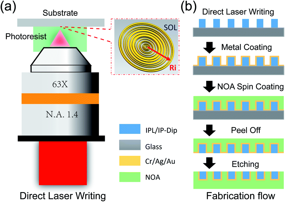 | ||
| Fig. 1 Schematic diagrams of direct laser writing (a) and fabrication flow of an SOL (b). | ||
Fabrication of an amplitude-modulated SOL
The fabrication flow of an amplitude-modulated SOL by inverse etching is shown in Fig. 1(b) and described in the Methods section. Morphologies of DLW-printed structures are determined by several key fabrication parameters such as mesh grid size, laser power (LP), scanning speed (SS), and substrates. To obtain high-quality printed patterns, different substrates and other fabrication parameters are explored and optimized in our experiments. Compromising high printing speed and minimum line width, the Galvo mode with a 63× objective is used in all laser writing processes.Substrates, pre-treatment, laser power and mesh grid size
To fabricate an amplitude-modulated SOL, metal films such as Cr, Ag or Au are usually used as an opaque mask to block the light. Considering the insoluble natures of cured IPL and IP-dip photoresists, the use of a photoresist to print an etching mask directly on a metal film followed by metal etching seems an easy approach to fabricate SOLs. Unfortunately, the patterns directly printed on Cr and Ag films have very poor quality. As shown in Fig. 2, the printed patterns suffer from poor line shape (a) and surface roughness (b and c) as well as missing parts (a and b) at sub-square boundaries. Similar effects occur when varied laser power (LP) is applied in printing (d–f). These problems are due to the high reflection and different surface properties of metals, which causes an increase in the interference intensity between the incident and reflected laser beams, and this affects the local light intensity above the substrate surface.23 As a result, it is very difficult to print directly on the metal films. | ||
| Fig. 2 Printed SOLs on glass/metal substrates with varied laser power, scanning speed and mesh grid size. Printed SOLs on substrates without silanization (a–c) with increased laser power on metal film (d–f) – (d) LP = 24 mW, (e) LP = 26 mW, (f) LP = 30 mW; SS = 10 mm s−1. Printed SOLs on glass cover slides (g–i) – (g) LP = 12 mW, (h) LP = 15 mW, (i) LP = 18 mW; SS = 6 mm s−1. Printed SOLs with increased mesh grid size (j) layer distance, 0.5 μm; contour number, 5; contour distance, 0.2 μm; and hatching distance, 0.2 μm. (k) Layer distance, 0.5 μm; contour number, 5; contour distance, 0.15 μm; and hatching distance, 0.2 μm. (l) Layer distance, 0.5 μm; contour number, 22; contour distance, 0.1 μm; and hatching distance, 0.2 μm. Contour line determines the laser spot along a route conformal to the surface of the structure. Scale bars in (a) and (b) are 40 μm, (c) and (j) are 4 μm, (d–i) are 10 μm, and (k) and (l) are 2 μm. | ||
To overcome or avoid the above-mentioned problems, dielectric substrates, which have been widely used and proved to be good substrates, were adopted. Hence, we printed patterns on dielectric substrates and then transferred the patterns onto the metal films. A method termed as inverse etching, as illustrated in Fig. 1(b), was proposed. In this process, problems faced by printing on a metal film were avoided without increasing fabrication complexity.
LP and SS as well as mesh grid density from the STL format in the DLW control software have significant influence on the final patterns, and all these factors are correlated to each other. Besides, substrate treatment also plays a vital role in the final patterns. We notice clear detachment of ring belts from dielectric substrates, mostly at the edges of the ring belts, if the substrates are not pretreated properly. In some extreme cases, a total writing area of the belts is detached; see Fig. 2(c) as an example. Moreover, outer rings usually suffer from more severe detachment than those in the centre. This detachment, attributed to the stress in the ring belts formed during the polymerization of a photoresist, can be eliminated by improved adhesion between photoresist ring belts and substrates. This is achieved by the silanization of substrate surfaces using 3-(trimethoxysilyl)propyl methacrylate before printing. Higher adhesion is required for ring-shaped patterns as they induce more stress inside the photoresist compared to linear patterns. Soaking in the 3-(trimethoxysilyl)propyl methacrylate solution affords chemical bonding between the substrate and polymerized photoresist, which can dramatically enhance the adhesion (see Fig. 2(g–l)).
We also found that metal films suffer from fewer adhesion problems, which is probably due to good heat conductivity and surface chemical properties of a metal. It should be noted that even after treatment by 3-(trimethoxysilyl)propyl methacrylate, vacancies still existed with varied LP.
Varied LP and mesh grid as well as scanning speed have been explored to produce SOLs, as indicated in Fig. 2 (g–l) and 3(e), (h) and (i). First, we set the scanning speed at 6 mm s−1 as an empirical parameter and then, we tune LP from 10 mW to 20 mW and choose a value that produces relatively high-quality patterns as the working LP; next, we optimize the mesh grid. In the experiment, LP = 18 mW results in relatively good morphology. Finally, we also investigate the effects of scanning speed on the quality of SOLs, which will be discussed in the next section.
 | ||
| Fig. 3 SEM images of printed patterns with high quality (a–c), with (d) and without displacements (e), after removing glass substrate and inspection of NOA transferring quality (f), after RIE etching of Cr film (g), relatively low scanning speed-induced connection between rings (h) and burrs on ring belt side wall (i). SOL produced by wet etching of Cr film after directly printing masks on the metal film (j). Scale bars in (a–c) are 100 μm, 40 μm and 10 μm and in (d), (e), (g–j) are 2 μm; (f) is 20 μm. | ||
Surface morphologies or roughness of the printed ring belts is largely dependent on mesh grid density, as seen in Fig. 2(j–l). This is important for the inverse etching method since metal film residue on top of these ring belts may act as an obstacle to scatter the light. Since the boundary lines between the contour line and hatching line can be clearly observed in Fig. 2(j and k), we use all contour lines to form ring belts as most ring belts in the SOL design are less than 4 μm in size. Thus, the contour number is set to 22, corresponding to ∼4.6 μm-wide lines. Layer distance is empirically set to 0.5 μm, which results in good SOL quality. Fused silica slabs and glass cover slides are used as substrates in our inverse etching process.
With optimized parameters, high quality patterns can be produced with stable reproducibility, and the parameters are LP = 18 mW, SS = 6 mm s−1, layer distance = 0.5 μm, contour number = 22, contour distance = 0.1 μm, and hatching distance = 0.2 μm (Fig. 3(a–e)). In the printed patterns, mismatches between different squares have been observed, as seen in Fig. 3(d–e). The statistics of displacements between different squares in both vertical (x) and longitudinal (y) directions are shown in Table 1. The origin and effect of these displacements on the SOL's focusing performance will be discussed below. In metal coating and PU infiltration processes, optical glue (NOA 61) completely infiltrates the gaps of the ring belts, and the metal film is in a complementary arrangement of SOL pattern after peeling off from the substrate, as depicted in Fig. 1(b) and 3(f).
| Direction | Displacement length | |||||
|---|---|---|---|---|---|---|
| Δ < 100 (nm) | 100 < Δ < 200 (nm) | 200 < Δ < 300 (nm) | 300 < Δ < 400 (nm) | 500 < Δ < 600 (nm) | Total number | |
| Vertical (x) direction | 11 ± 5 | 10 ± 3 | 6 ± 2 | 3 ± 2 | 0 | 30 |
| Longitudinal (y) direction | 15 ± 5 | 11 ± 3 | 3 ± 1 | 1 ± 1 | 0 | 30 |
To further explore the inverted structure, we scratch the inverted surface, as shown in Fig. 3(f). The dark cracked areas are printed ring belts, and the bright areas correspond to the deposited metal films. As we expected, the inverted surface is totally flat, and the inverted structure of the printed patterns can be obtained without any clear damage.
Etching conditions and scanning speed
According to the inverted mask fabrication scheme shown in Fig. 1(b), lateral etching can be largely eliminated if the metal film deposition is highly directional and thus, sidewalls of the printed structures can be free of the metal film. Hence, the method gives good tolerance for wet etching time where lateral etching is concerned. Even if the sidewalls are coated with a thin layer of metal film, their etching rate in an extremely narrow gap is rather slow. Moreover, the printed structures have a height of 2 μm and thus, the process is tolerant to wet etching time in the experiments. This method has remarkable advantage over the traditional mask etching method in which lateral etching is inevitable. As an alternative etching approach, argon-reactive ion etching of Cr/Ag can also be used to remove metals from the top surface, but the etching selectivity for Cr with argon and a photoresist is low, as shown in Fig. 3(g). Similar to that observed for wet etching, the ending points in this etching process also exhibit much more tolerance.Another interesting finding is that during the etching process, we could clearly observe that the roughness of the sidewalls was sensitive to SS when SS was in the range from 3 mm s−1 to 6 mm s−1 with an interval of 1 mm s−1. High SS for the same LP value resulted in thinner line width, whereas low SS could produce some burrs on the sidewall of the ring belts (Fig. 3 (h–i)), which contributed to slightly increased exposure dose of light. Please note that the polarization effect needs to be taken into account while fabricating high resolution structures, for example, when the line width is reduced to 250 nm in our case.24 As a result, carefully adjusted LP and SS as well as mesh grid size are essential to produce high-quality SOLs. For a direct comparison with our wet etching method, an SOL formed by directly printing on metal film is shown in Fig. 3(j), and its quality is poor as expected.
Random displacement-induced focusing performance degradation
Even after using the optimized fabrication parameters, we observe that displacements between the adjacent squares of printed patterns still exist. We have checked all the displacements between divided squares of three printed SOLs by examining their optical and SEM images, and the results are summarized in Table 1. All the three SOLs printed with the same optimized parameters have good quality, but they exhibit displacements; the displacements are found to be randomly distributed. For the Galvo mode, the area printed in a certain time is limited to the objective, and the maximum value is 130 μm in diameter for 63× objective with Cartesian coordinates. Therefore, larger patterns should be split into several parts, and multiple printings are required, which inevitably results in random displacements less than 1 μm in size between adjacent square regions during movements. To evaluate the influence of the random displacements on focus performance of SOLs, angular spectrum simulations are performed by assuming a random shift, Δ, in both vertical (x) and longitudinal (y) directions in each square. To fit the experimental conditions, an SOL with a diameter of 600 μm in the simulation is divided into squares with dimensions of 7 × 7 with a side length of 110 μm. We assume that| x = xi + rand(0,Δ) |
| y = yj + rand(0,Δ) |
To evaluate the optical qualities of the printed SOLs, we studied their focusing performance. A linearly polarized laser beam with 633 nm wavelength was projected on a fabricated binary amplitude SOL and its optical and scanning electron images are given in Fig. 4(a), (b) and (c), respectively. After transmitting through the SOL, the theoretical focusing performance was calculated using the angular spectrum method. A needle-like focus could be observed at a distance of 100 μm from the SOL plane, as seen from Fig. 4(d); its transverse spot size in terms of FWHM was around 0.42λ within the depth of focus of 6 μm in the axial direction, which can be inferred from Fig. 4(e). This corresponded to an effective numerical aperture of NAeff = 1.19 using the definition of FWHM = λ/2NAeff. In the experiment, we observed bright foci at several sliced focal distances (98 μm, 100 μm, and 102 μm), as shown in Fig. 4(h), and the focus did not change much across an axial distance over ±3 μm; these results agreed well with the simulation results given in Fig. 4(g). Considering the pixel size of the camera (5.3 μm) and magnification of the imaging system (500×), the effective pixel size in the experiment was found to be 10.6 nm, and the average spot size was estimated to be 0.45λ, which was slightly larger than the simulation results, but it was still in the sub-diffraction level as designed. Another finding was that the ring shape sidebands, which were clearly observed in the simulation, become distorted; this can be explained by the slight misalignment of incoming light, fabrication imperfection of the sample, and in particular by displacement. The simulation results on the focusing performance at several random displacements with Δ = 0, 100 nm, 200 nm, 300 nm, 400 nm and 600 nm are shown in Fig. 4(i), and they were based on the model shown in Fig. 4(f); these results confirmed that the random displacements did not affect the focal spot dramatically when they were below 400 nm.
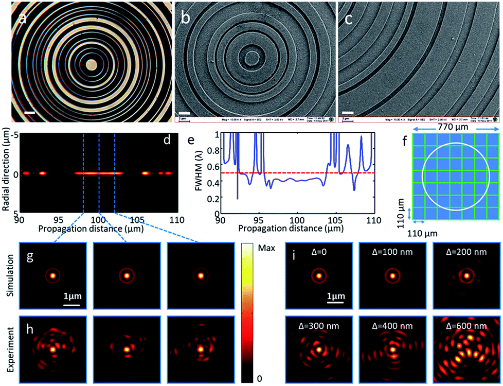 | ||
| Fig. 4 Optical (a) and scanning electron (b and c) images of amplitude-modulated SOLs. Simulated (d, e and g) and experimental (h) focusing properties of the SOLs. (f and i) Angular spectrum calculated diffraction patterns of SOLs with displacements between squares randomly distributed in range of 0–Δ, Δ = 0, 100 nm, 200 nm, 300 nm, 400 nm and 600 nm at z = 100 μm at 633 nm. Scale bars in (a–c) is 2 μm. | ||
Near the focal plane of z = 100 μm, the intensity ratio between the highest sideband and the central spot observed in the experiment ranges from 35% to 48%, which is in reasonable agreement with the simulated counterparts of 45% (Δ = 300 nm), 28% (Δ = 200 nm) and 23% (Δ = 100 nm). In the ideal case (Δ = 0), the simulated ratio is 19.8%, which is much lower than the experimental data. Above 600 nm (around one wavelength), the focusing performance degrades considerably due to the increased random phase noise in shaping the focus.
Binary phase SOL
To improve the transmission efficiency, in addition to binary amplitude SOLs, a transparent binary phase SOL with alternating ‘0’ and ‘π’ phase modulated zones has also been manufactured by the DLW method but with reduced procedures. Only two steps, printing and etching, are involved as the metal film is replaced by dielectric materials. Moreover, dry etching, such as reactive ion etching (RIE), is applied to remove the dielectric film and to achieve high precision in etching depth. Here, Si3N4 film with a refractive index of 1.917 is selected as a phase delay film. For 633 nm wavelength, 345 nm-thick Si3N4 film deposited on silica substrate is used to create the binary phase delay. The optical and SEM images of the fabricated SOL are shown in Fig. 5(a), (b) and (c), respectively. After mask pattern printing and RIE etching, the residual photoresist mask on Si3N4 ring belts is removed by O2 plasma etching, as shown in Fig. 5(d–f). Few particle residuals can be observed on Si3N4 after O2 etching, which is probably due to carbon or undissolved photoresist in the etching process.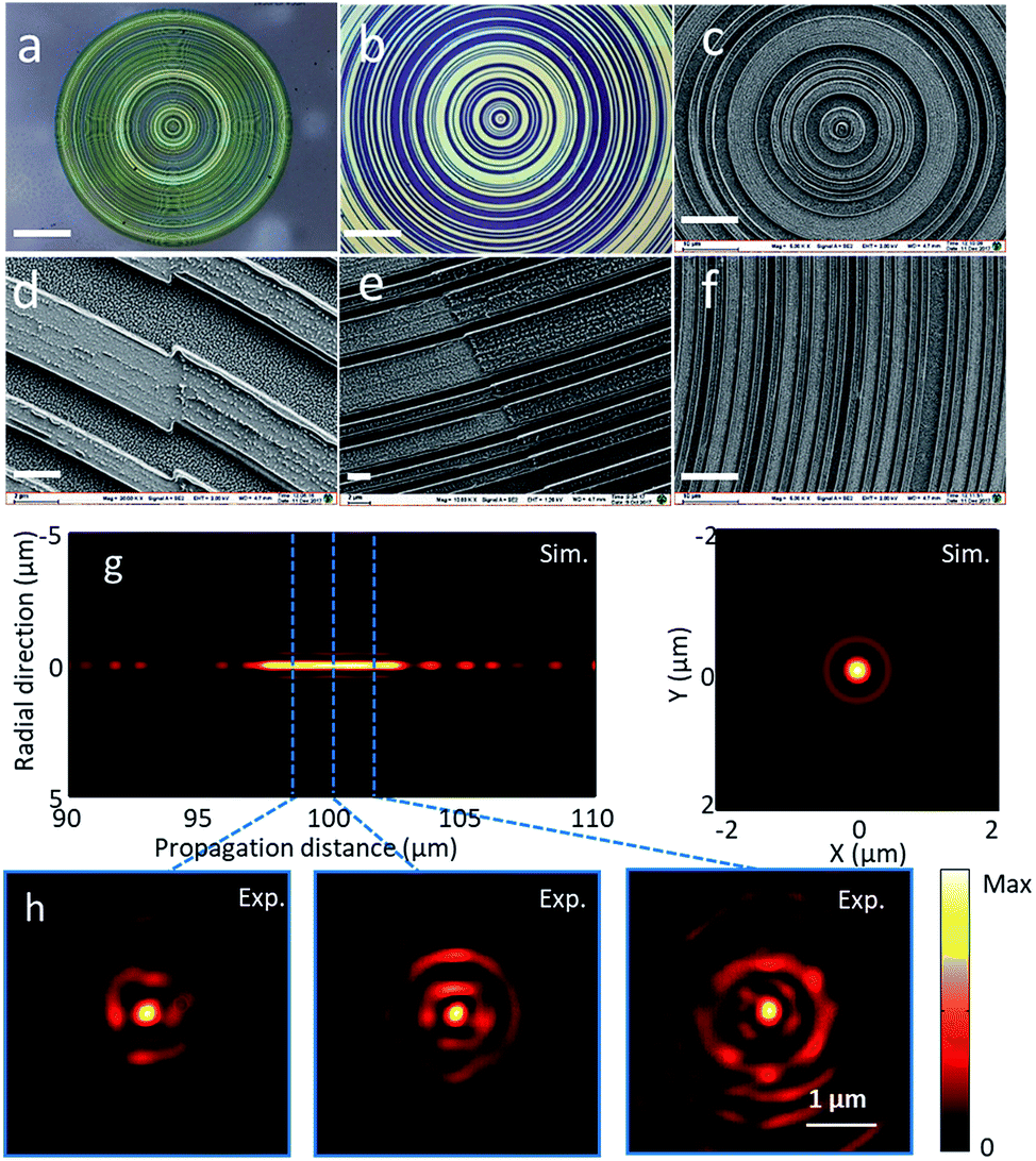 | ||
| Fig. 5 Characteristics of binary phase SOL. (a) and (b) optical microscope images, (c–f) SEM images at varied magnification. (g) Simulated focusing properties of SOLs in the longitudinal (left) and transverse (right, z = 100 μm) cross-sections. The three experimental images in (h) are taken at z = 98 μm, 100 μm, and 102 μm, respectively. Scale bars in (a–c) are 150 μm, 20 μm and 10 μm and in (d–f) are 2 μm, 2 μm and 10 μm. | ||
As evidenced by experimental results, the particle residues do not dramatically affect the focusing performance of SOLs because their sizes are less than 100 nm. Experimentally, the measured needle-like focus created by the binary phase SOL, as shown in Fig. 5(h), is ∼0.46λ in FWHM, and the depth of focus is ∼6 μm at a focal distance of ∼100 μm, which is in accordance with the simulation results, as shown in Fig. 5(g).
Conclusion
In conclusion, SOLs with a large diameter (up to 600 μm) and an effective numerical aperture of 1.19 have been successfully produced by the direct laser writing method with a smallest line width resolution of 1 μm. Substrate effects, laser power, scanning speed, and mesh grid size dependence are well investigated, and high-quality ring belts on dielectric substrates are obtained with the following optimized printing parameters: LP = 18 mW, SS = 6 mm s−1, layer distance = 0.5 μm, contour number = 22, contour distance = 0.1 μm, and hatching distance = 0.2 μm. Though random displacements between squares constituting the SOL cannot be avoided, focus spot size can be retained when the displacement is below 400 nm. As a complementary sub-micrometre fabrication method between traditional lithography and nanofabrication method, DLW can be a promising approach to manufacture SOLs, and this method has the advantages of relatively high speed, low equipment volume, less complexity and sub-micrometre lateral resolution.Methods
Fabrication flow of amplitude and phase SOLs
Photonic Professional GT (Nanoscribe GmbH) was used to print the SOL masks. The operation laser was 780 nm in wavelength. The peak irradiance at the focal spot could be calculated by the power, P, the pulse width, τ, and the repetition rate, f, of the laser:25,26Here, the unit of I0 is GW cm−2. The beam waist, ω0, with a 3D Gaussian distribution could be calculated as 480 nm. In our experiments, the pulse width is τ = 180 fs, and the repetition rate is f = 80 MHz. First, SOL patterns were printed on a glass cover slip using IPL/IP-dip photoresist by DLW. The patterns were first molded by the 3D drawing software according to designed results and then meshed through the Describe software. Cover slips were silanized with 3-(trimethoxysilyl)propyl methacrylate (Sigma) for half an hour before use to increase adhesion between substrates and photoresist. Then, the cover slip was coated with a layer of 150 nm-thick Ag/Cr film by e-beam evaporation, followed by spin coating a layer of polymer (NOA 61, PU) on the pattern and then curing by UV light for 30 s. A piece of PMMA as the supporting substrate was placed on PU before UV curing. After this, PU was peeled from the glass cover slide substrate. Alternatively, the glass substrate could be etched by HF solution to release the PU film. Finally, the PU film was placed bottom up, and the top bare metal layer was removed by wet etching. A chromium wet etching solution, which consisted of ceric ammonium nitrate
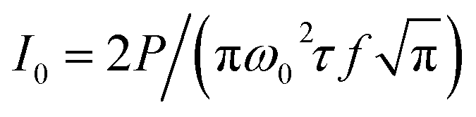
![[thin space (1/6-em)]](https://www.rsc.org/images/entities/char_2009.gif) :perchloric acid:H2O = 10.9%:4.25%:84.85%, was used in the wet etching process. Etching rates for Cr and Ag were ∼2 nm s−1 and 5 nm s−1, respectively. Thus, we obtained amplitude-modulated SOLs. We required 16 minutes to print one 600 μm-diameter SOL, 25 minutes to develop it, and about three hours for metal film deposition using e-beam evaporation. The following procedures including transferring SOL to NOA substrate and metal film etching required about 10–20 minutes. Thus, the total time for writing an SOL was typically around 4 hours. Since the height of a printed SOL was set to 2 μm throughout the experiments, a further decrease in the height decreased the printing time proportionally. Moreover, for phase SOLs, the printed structure only acts as an etching mask, morphologies of the top surface of printed SOL did not affect the final SOL quality; thus, a further increase in the mesh grid size could decrease the overall printing time.
:perchloric acid:H2O = 10.9%:4.25%:84.85%, was used in the wet etching process. Etching rates for Cr and Ag were ∼2 nm s−1 and 5 nm s−1, respectively. Thus, we obtained amplitude-modulated SOLs. We required 16 minutes to print one 600 μm-diameter SOL, 25 minutes to develop it, and about three hours for metal film deposition using e-beam evaporation. The following procedures including transferring SOL to NOA substrate and metal film etching required about 10–20 minutes. Thus, the total time for writing an SOL was typically around 4 hours. Since the height of a printed SOL was set to 2 μm throughout the experiments, a further decrease in the height decreased the printing time proportionally. Moreover, for phase SOLs, the printed structure only acts as an etching mask, morphologies of the top surface of printed SOL did not affect the final SOL quality; thus, a further increase in the mesh grid size could decrease the overall printing time.
For the phase-modulated SOLs, to remove Si3N4 by RIE, 10 sccm CF4 and 20 sccm CHF3 were used as etching gases. The etching pressure was set at 5 Pa, and power was set at 350 W. The etching rate was ∼5 nm s−1. O2 RIE parameter was 80 sccm O2, 10 Pa, and power was 150 W. Usually, we required 3–5 minutes to remove residual photoresists from Si3N4.
Design and characterization of SOL
For the design of SOLs, we use the binary particle swarm optimization (BPSO) algorithm,21,27 which optimizes a problem regarding a given merit function using a population of ‘particles’ in the N-dimensional search space. For a ring mask, the radial direction is divided into N equally spaced zones. Each zone has either a unit (‘1’) or zero (‘0’) value, which corresponds to transparent or opaque for the amplitude modified mask and two phase levels ‘0’ or ‘π’ for the phase-modified mask. The BPSO algorithm searches for the best arrangement of these binary values. As a result, a designed SOL usually consists of a series of concentric ring belts with different widths and radii. We choose a diameter of 600 μm for moderate fabrication time and ease of optical characterization.To characterize the performance of SOLs, linearly polarized 633 nm laser beam was impinged on the SOL, and the focused light was collected by a 150× objective lens (NA = 0.95), subsequently magnified an additional 4 times with a telescope system and finally imaged by a CMOS camera. The effective magnification was 500 after calibration. Since super-oscillatory focus is formed by interference of propagating waves, it can be projected and imaged into the optical far-field region.
Conflicts of interest
The authors declare no conflict of interest.Acknowledgements
Haibin Ni and Guanghui Yuan contributed equally. We would like to thank Dr Hongcheng Gu, Haibo Ding and Liuxiao Jiang for useful suggestions for printing. We also thank Dr Muhammad Shemyal Nisar for language polishing. This work was financially supported by the National Key Research and Development Program of China (No. 2017YFA0205700), National Natural Science Foundation of China (Grants 21373046, 61605082 and 21327902), the Natural Science Foundation of Jiangsu Province (BK20160969), the Natural Science Foundation of the Jiangsu Higher Education Institutions of China (16KJB510020), and the Priority Academic Program Development of Jiangsu Higher Education Institutions (PAPD). China Postdoctoral Science Foundation Funded Project (2017M611654). Jiangsu Postdoctoral Science Foundation Funded Project (1701074B). The Startup Foundation for Introducing Talent of NUIST (2015r040). Open Project of Jiangsu Key Laboratory of Meteorological Observation and Information Processing under Grant KDXS1506. Jiangsu Science and Technology Department (Grant No. BE2014707), the Program for New Century Excellent Talents in University, Fundamental Research Funds for the Central Universities, and Six Talent Peaks Project of Jiangsu Province. GHY would like to thank the financial support from the Singapore Ministry of Education (Grant MOE2011-T3-1-005), ASTAR QTE Programme Grant (SERC A1685b0005) and useful suggestions from Prof Nikolay Zheludev.Notes and references
- E. T. Rogers, J. Lindberg, T. Roy, S. Savo, J. E. Chad, M. R. Dennis and N. I. Zheludev, Nat. Mater., 2012, 11, 432–435 CrossRef PubMed.
- T. Roy, E. T. F. Rogers, G. H. Yuan and N. I. Zheludev, Appl. Phys. Lett., 2014, 104, 231109 Search PubMed.
- G. Chen, Y. Li, A. Yu, Z. Wen, L. Dai, L. Chen, Z. Zhang, S. Jiang, K. Zhang, X. Wang and F. Lin, Sci. Rep., 2016, 6, 29068 CrossRef PubMed.
- Z. Gan, Y. Cao, R. A. Evans and M. Gu, Nat. Commun., 2013, 4, 2061 CrossRef PubMed.
- F. Qin, K. Huang, J. F. Wu, J. H. Teng, C. W. Qiu and M. H. Hong, Adv. Mater., 2017, 29, 1602721 CrossRef PubMed.
- B. K. Singh, H. Nagar, Y. Roichman and A. Arie, Light: Sci. Appl., 2017, 6, e17050 CrossRef.
- G. H. Yuan, E. T. F. Rogers, T. Roy, G. Adamo, Z. X. Shen and N. I. Zheludev, Sci. Rep., 2014, 4, 6333 CrossRef PubMed.
- G. Yuan, E. T. Rogers, T. Roy, Z. Shen and N. I. Zheludev, Opt. Express, 2014, 22, 6428–6437 CrossRef PubMed.
- X. Chen, M. Chen, M. Q. Mehmood, D. Wen, F. Yue, C.-W. Qiu and S. Zhang, Adv. Opt. Mater., 2015, 3, 1201–1206 CrossRef.
- J. S. Diao, W. Z. Yuan, Y. T. Yu, Y. C. Zhu and Y. Wu, Opt. Express, 2016, 24, 1924–1933 CrossRef PubMed.
- T. Liu, Q. Liu, S. M. Yang, Z. D. Jiang, T. Wang and X. K. Yang, Opt. Commun., 2017, 393, 72–76 CrossRef.
- E. T. F. Rogers, S. Savo, J. Lindberg, T. Roy, M. R. Dennis and N. I. Zheludev, Appl. Phys. Lett., 2013, 102, 031108 CrossRef.
- S. S. Stafeev, A. G. Nalimov, M. V. Kotlyar, D. Gibson, S. Song, L. O'Faolain and V. V. Kotlyar, Opt. Express, 2016, 24, 29801–29814 CrossRef PubMed.
- A. P. Yu, G. Chen, Z. H. Zhang, Z. Q. Wen, L. R. Dai, K. Zhang, S. L. Jiang, Z. X. Wu, Y. Y. Li, C. T. Wang and X. G. Luo, Sci. Rep., 2016, 6, 38859 CrossRef PubMed.
- Y. H. Zhang, W. H. Zhong, D. M. Liu, Y. Zhang, M. Xiao and IEEE, in 2016 Conference on Lasers and Electro-Optics, 2016 Search PubMed.
- G. Chen, K. Zhang, A. P. Yu, X. Y. Wang, Z. H. Zhang, Y. Y. Li, Z. Q. Wen, C. Li, L. R. Dai, S. L. Jiang and F. Lin, Opt. Express, 2016, 24, 11002–11008 CrossRef PubMed.
- G. H. Yuan, E. T. F. Rogers and N. I. Zheludev, Light: Sci. Appl., 2017, 6, e17036 CrossRef.
- Q. Wang, E. T. F. Rogers, B. Gholipour, C.-M. Wang, G. Yuan, J. Teng and N. I. Zheludev, Nat. Photonics, 2015, 10, 60–65 CrossRef.
- G. H. Yuan, E. T. F. Rogers, B. Lafferty, M. Mooney, Z. X. Shen, N. I. Zheludev and IEEE, in 2013 Conference on Lasers and Electro-Optics, 2013 Search PubMed.
- P. Genevet, F. Capasso, F. Aieta, M. Khorasaninejad and R. Devlin, Optica, 2017, 4, 139 CrossRef.
- G. Chen, Y. Li, X. Wang, Z. Wen, F. Lin, L. Dai, L. Chen, Y. He and S. Liu, IEEE Photonics Technol. Lett., 2016, 28, 335–338 CrossRef.
- A. Balcytis, D. Hakobyan, M. Gabalis, A. Zukauskas, D. Urbonas, M. Malinauskas, R. Petruskevicius, E. Brasselet and S. Juodkazis, Opt. Express, 2016, 24, 16988–16998 CrossRef PubMed.
- S. Rekštytė, T. Jonavičius and M. Malinauskas, Opt. Lasers Eng., 2014, 53, 90–97 CrossRef.
- S. Rekštytė, T. Jonavičius, D. Gailevičius, M. Malinauskas, V. Mizeikis, E. G. Gamaly and S. Juodkazis, Adv. Opt. Mater., 2016, 4, 1209–1214 CrossRef.
- L. Jonušauskas, S. Juodkazis and M. Malinauskas, J. Opt., 2018, 20, 053001 CrossRef.
- H. Ding, Q. Zhang, Z. Gu and M. Gu, Nanoscale Horiz., 2018, 3, 312–316 RSC.
- N. Jin and Y. Rahmat-Samii, Journal of Artificial Evolution and Applications, 2008, 2008, 1–10 CrossRef.
Footnote |
| † The two authors contributed equally. |
| This journal is © The Royal Society of Chemistry 2018 |