
 Open Access Article
 This Open Access Article is licensed under a
 Creative Commons Attribution 3.0 Unported Licence
Ambipolar organic phototransistors based on 6,6′-dibromoindigo†
Hyoeun Kima,
Gyoungsik Kimb,
Inho Songa,
Jungho Leeb,
Hanum Abdullaha,
Changduk Yang *b and
Joon Hak Oh*a
*b and
Joon Hak Oh*a
aDepartment of Chemical Engineering, Pohang University of Science and Technology (POSTECH), Pohang, Gyeongbuk 790-784, South Korea. E-mail: joonhoh@postech.ac.kr
bDepartment of Energy Engineering, School of Energy and Chemical Engineering, Perovtronics Research Center, Low Dimensional Carbon Materials Center, Ulsan National Institute of Science and Technology (UNIST), 50 UNIST-gil, Ulju-gun, Ulsan 44919, South Korea. E-mail: yang@unist.ac.kr
First published on 19th April 2018
Abstract
Ambipolar organic phototransistors were fabricated using a natural pigment 6,6′-dibromoindigo (6-BrIG) as the active channel. These phototransistors yielded significantly enhanced currents upon light illumination with photoresponsivities and external quantum efficiencies as high as 10.3 A W−1 and 2437% for the n-channel, and 55.4 mA W−1 and 13.1% for the p-channel, respectively. In addition, simple inverter complementary circuits were fabricated by integrating two ambipolar phototransistors. Channel current was dependent on light intensity and voltage bias. This study provides a basis for an in-depth understanding of the optoelectronic characteristics of 6-BrIG, and introduces this material as an ecofriendly candidate for optoelectronic applications.
1. Introduction
Organic π-conjugated materials have received much attention due to their tunable optical and electrical properties, suitability for flexible device fabrication, and large-area processability.1–3 Organic field-effect transistors (OFETs),4,5 organic light-emitting diodes (OLEDs),6 organic phototransistors (OPTs),7–9 organic photovoltaics (OPVs),10,11 organic memories,12 and organic sensors13 have been successfully developed. Phototransistors, which allow one to control channel conductance via light absorption, are particularly applicable to electronic devices such as light sensors and optical switches.14 Although many research groups have reported phototransistors with unipolar characteristics,15–19 few have explored ambipolar phototransistors, which have mostly been demonstrated using blend,20 heterojunction,21,22 or complementary logic circuits23 made by sequentially processing two p- and n-type semiconductors. Phototransistors based on ambipolar materials, which are single component systems that can function as both p- and n-type semiconductors, have also been demonstrated.24–27 Single component, ambipolar transistors are cost-effective and boast several advantages including large-area applicability and simple fabrication. Despite their advantages, research on ambipolar material-based phototransistors is insufficient. Therefore, new photoconductive ambipolar materials must be developed to improve our understanding of their photophysical properties and suitability for practical applications.In this work, we investigated the use of a natural pigment, 6,6′-dibromoindigo (6-BrIG or tyrian purple), as an ambipolar semiconductor for use in phototransistors. 6-BrIG is a well-known chromophore and is the oldest known purple dye, extracted from sea snails. Interestingly, this material has several unique properties that match well with the requirements of electronic devices.28–30 6-BrIG boasts (i) a small bandgap energy of 1.8 eV for balanced ambipolar charge injection, (ii) a relatively deep-lying lowest unoccupied molecular orbital (LUMO) level of −3.7 eV for air-stable electron transport, (iii) strong intra- and intermolecular hydrogen bonding between its amine and carbonyl groups; this induces planarity and short π–π stacking distances, which are beneficial for efficient charge transport, and (iv) non-toxicity and biocompatibility.29 Although ambipolar OFETs and inverter circuits based on 6-BrIG have been demonstrated,31–33 early studies have been confined to its use in transistors.
The small bandgap and broad absorption band (350–700 nm) of 6-BrIG imply facile excitation from the highest occupied molecular orbital (HOMO) to the LUMO upon exposure to visible light. We therefore introduced 6-BrIG into phototransistors as an ambipolar organic semiconductor. Ambipolar charge transport was observed in the dark and was significantly enhanced upon exposure to light. This indicated that 6-BrIG functioned as a photoactive layer. OPTs based on 6-BrIG exhibited photoresponsivity as high as 10.3 A W−1 and remarkable external quantum efficiency of 2437% under light illumination.
2. Experimental
2.1 Instruments
6-BrIG was synthesized in accordance with previously published procedures.34,35 1H NMR spectra were recorded on a Varian VNRS 400 MHz (Varian USA) spectrophotometer using CDCl3 as the solvent and tetramethylsilane (TMS) as the internal standard. UV-vis spectra were acquired on a Cary 5000 spectrophotometer. Cyclic voltammetry (CV) was performed on an AMETEK VersaSTAT 3 with a three-electrode cell in a nitrogen-purged solution of 0.1 M tetra-n-butylammonium hexafluorophosphate (n-Bu4NPF6) in acetonitrile at a scan rate of 0.1 V s−1 at room temperature. A platinum wire, Ag/Ag+ (0.01 M of AgNO3 in acetonitrile) electrode, and 6-BrIG deposited onto ITO-coated glass were used as the counter electrode, reference electrode, and working electrode, respectively. The Ag/Ag+ reference electrode was calibrated using a ferrocene/ferrocenium redox couple as an external standard, whose oxidation potential was set at −4.8 eV with respect to the zero vacuum level. The HOMO energy level was obtained from the equation HOMO = −(Eonsetox − Eonsetferrocene + 4.8) eV. The LUMO level was obtained from the equation LUMO = HOMO + Eoptg eV.2.2 Synthesis of 6-bromo-3-iodoindole (1)
Iodine (2.59 g, 10.2 mmol) was added to a solution of 6-bromoindole (2 g, 10.2 mmol) and sodium hydroxide (0.41 g, 10.2 mmol) in methanol (100 mL) and an aqueous potassium iodide (1.69 g, 10.2 mmol) solution (10 mL). The reaction mixture was stirred at room temperature for 3 h and water was added. The resulting precipitate was collected by filtration, washed with water, and dried under reduced pressure. The product 6-bromo-3-iodoindole was used for the following reaction without purification.2.3 Synthesis of 3-acetoxy-6-bromoindole (2)
Silver acetate (1.56 g, 9.32 mmol) was added to a solution of 6-bromo-3-iodoindole (2 g, 6.21 mmol) in glacial acetic acid (50 mL). The reaction mixture was stirred at 90 °C for 2 h and the mixture was cooled to room temperature and filtered. The crude product was purified by column chromatography (silica gel, dichloromethane) to afford 0.88 g (56%) of 3-acetoxy-6-bromoindole. 1H NMR (400 MHz, CDCl3) δ (ppm) 7.89 (br, 1H), 7.47 (d, 1H, J = 1.6 Hz), 7.42 (d, 1H, J = 8.4 Hz), 7.32 (d, 1H, J = 2.8 Hz), 7.25 (dd, 1H, J1 = 8.4 Hz, J2 = 1.6 Hz), 2.36 (s, 3H). GC-DIP/MS (m/z) calcd: 254.08; found: 254.7. EA: anal. calcd for C10H8BrNO2: C, 47.27; H, 3.17; N, 5.51; found: C, 47.11; H, 3.31; N, 5.37.2.4 Synthesis of 6,6′-dibromoindigo (6-BrIG)
1 M sodium hydroxide solution (10 mL) was added to a solution of 3-acetoxy-6-bromoindole (0.88 g, 3.47 mmol) in ethanol (30 mL). Water was added to the mixture after stirring at room temperature for 3 h. The resulting precipitate was collected by filtration and washed several times with water and cold ethanol. The resulting purple solid was dried under vacuum and combined to give a purple solid as 6,6′-dibromoindigo (0.55 g, 75%). NMR peaks were not detected due to limited solubility in various solvents. IR νmax (solid)/cm−1: 3385 (N–H), 1633 (C![[double bond, length as m-dash]](https://www.rsc.org/images/entities/char_e001.gif) O), 1610 (CC). GC-DIP/MS (m/z) calcd: 420.05; found: 419.9. EA: anal. calcd for C16H8Br2N2O2: C, 45.75; H, 1.92; N, 6.67; found: C, 45.50; H, 1.71; N, 6.51.
O), 1610 (CC). GC-DIP/MS (m/z) calcd: 420.05; found: 419.9. EA: anal. calcd for C16H8Br2N2O2: C, 45.75; H, 1.92; N, 6.67; found: C, 45.50; H, 1.71; N, 6.51.
2.5 Device fabrication
Devices were fabricated with a bottom-gate top-contact configuration. Commercially available, thermally grown, 300 nm-thick SiO2 on highly n-doped Si (100) (<0.004 Ω cm) was used as the device substrate. Si functioned as both the substrate and the gate electrode, and SiO2 acted as the gate dielectric with a capacitance per unit area of 10 nF cm−2. The SiO2 surface was modified with an n-octadecyltrimethoxysilane (OTS) self-assembled monolayer according to a reported method.36 The OTS-treated wafers were rinsed with toluene, acetone and isopropyl alcohol, and dried under a stream of N2. For the channel layer, 6-BrIG was deposited by thermal evaporation under high vacuum (<5.0 × 10⁻⁶ torr, Tsubstrate = 80 °C, rate = 0.1–0.3 Å s−1, and film thickness = 30 nm). Thermal annealing was carried out at 100 °C for 30 min in an N2 atmosphere. Au top-contact electrodes (40 nm) were thermally evaporated through a shadow mask with a channel width–length ratio (W/L) of 17.5.2.6 Measurement of OFETs and OPTs
Electrical performance was recorded in a N2-filled glovebox using a Keithley 4200 semiconductor parametric analyzer due to their low air-stability. Optoelectronic properties were measured in a vacuum chamber using monochromic and polychromic light sources.3. Results and discussion
3.1 Synthesis and characterization
The synthetic procedures to obtain intermediates and the target molecule (6-BrIG) are outlined in Scheme 1, which were prepared according to the literatures.34,35 Briefly, 3-acetoxy-6-bromoindole (2) was synthesized by sequential reactions, i.e., iodination of 6-bromoindole and nucleophilic substitution with silver acetate, followed by hydrolysis with a sodium hydroxide solution in ethanol, affording 6-BrIG in a 25.7% overall yield. Detailed synthetic routes and characterization can be found in the Experimental section and ESI.† The synthesized 6-BrIG showed limited solubility in common organic solvents, mainly due to strong intramolecular hydrogen bonding. Thus, 6-BrIG was difficult to characterize by NMR. Therefore, the structural characteristics and elemental composition of the synthesized 6-BrIG were verified by mass spectrometry. Both were consistent with calculated values. In addition, the infrared absorption spectrum of 6-BrIG contained stretching vibrations at 3385, 1633, and 1610 cm−1, corresponding to N–H, CO, and CC bonds, respectively. Thermogravimetric analyses revealed a high thermal stability with a decomposition temperature of 346 °C, which corresponded to a 5% weight loss (see Fig. S1 and S2 in ESI†).
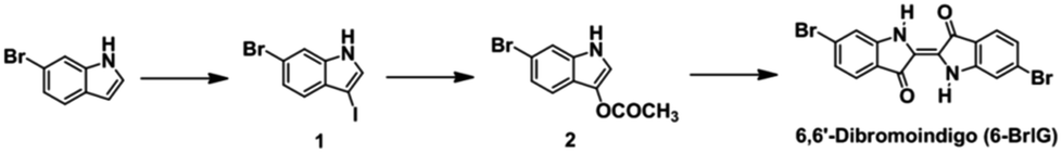 | ||
| Scheme 1 Synthetic routes to 6-BrIG. | ||
The UV-vis absorption spectrum of a 6-BrIG thin film is shown in Fig. 1a and the corresponding spectral data are summarized in Table 1. Interestingly, despite its small structure, 6-BrIG exhibited a broad absorption band from 350–700 nm, which can be attributed to a combination of the H-chromophore and a complex set of intramolecular interactions induced by the indigo core,37–39 and an absorption maximum (λmax) at 523 nm. The estimated optical bandgap (Eoptg) of 6-BrIG was 1.82 eV.
 | ||
| Fig. 1 (a) UV-vis absorption spectrum of 6-BrIG film. (b) Cyclic voltammogram of 6-BrIG film evaporated on ITO. (c) Schematic device structure of the phototransistor. | ||
| λfilmmax (nm) | Eoptga (eV) | EHOMOb (eV) | ELUMOc (eV) | |
|---|---|---|---|---|
| a Calculated from the absorption band edge of the thin film, Eoptg = 1240/λedge.b Vacuum deposited thin film in 0.1 M CH3CN/n-Bu4NPF6, versus ferrocene/ferrocenium at 0.1 V s−1. Energy level of HOMO estimated from the onset oxidation potentials, assuming the absolute energy level of ferrocene/ferrocenium to be 4.8 eV below vacuum.c ELUMO (eV) = EHOMO + Eoptg. | ||||
| 6-BrIG | 523 | 1.82 | −5.49 | −3.67 |
Cyclic voltammetry (CV) was conducted with a working electrode consisting of thermally evaporated 6-BrIG on indium tin oxide (ITO)-coated glass. An n-Bu4NPF6 solution was used as the electrolyte and ferrocene was employed as an external standard (Fig. 1b). The HOMO level was determined as the first onset potential of the oxidation peak at 0.86 V, but no reduction peak was observed in the potential range. The HOMO level of 6-BrIG, calculated using the equation EHOMO = −(Eonsetox − Eonsetferrocene + 4.8) eV, was −5.49 eV and the LUMO level, calculated with Eoptg, was −3.67 eV. These energy levels are commensurate with ambipolar charge transport in OFETs.
The surface morphology of 6-BrIG films was investigated via tapping-mode atomic force microscopy (AFM) before and after annealing at 100 °C for 30 min (Fig. 2). Thin films of 6-BrIG consisted of large, crystalline, needle-like grains with an average length of 1.16 μm. After annealing, a relatively more uniform and flatter surface was formed, with a root-mean-square (rms) roughness of 8.56 nm, much lower than that of the as-cast film (13.3 nm). This result indicates an enhancement of intermolecular packing and charge transport after the thermal annealing.
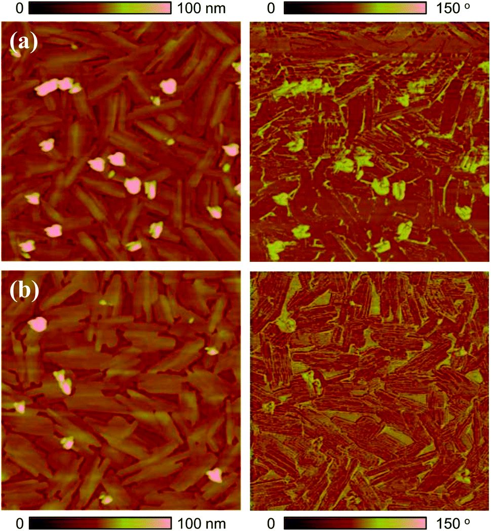 | ||
| Fig. 2 Tapping-mode AFM height (left) and phase (right) images (5 μm × 5 μm) of 6-BrIG films on OTS-treated SiO2/Si substrates: (a) as-cast and (b) annealed film at 100 °C. | ||
| IDS = 1/2(W/L)μCi(VGS − VTH)2 | (1) |
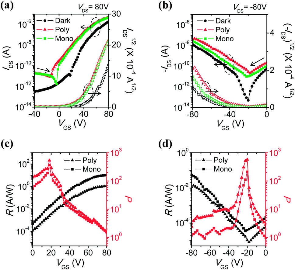 | ||
| Fig. 3 Transfer characteristics, photoresponsivity (R), and photocurrent/dark-current ratio (P) of 6-BrIG film in the dark and under illumination: (a and c) n-dominant operation, sweep from −80 to 80 V and (b and d) p-dominant operation, sweep from 80 to −80 V. The circle, triangle, and square symbols represent the dark, polychromic, and green monochromic light, respectively. | ||
Under light irradiation, off-currents significantly increased in both electron- and hole-enhancement modes due to the creation and dissociation of photogenerated excitons. Therefore, the on/off ratios under illumination became smaller, from 107 to 105–106 for n-channel transport, and from 105 to 103 for p-channel transport. In addition, mobilities were enhanced and the threshold voltages shifted negatively in the n-channel (or positively in the p-channel), meaning the easier turn-on of the device. This can be attributed to a decrease in the density of trap sites by photogenerated charge carriers.43,44 The amount of electrons (or holes) increases owing to the active charges coming from the additional photogenerated charge carriers, not only from gate-induced effects.
Photoresponsivity (R) and the photocurrent/dark-current ratio (P) are quantitative parameters for the sensitivity of OPTs. These values were calculated by the following eqn (2) and (3):
| R = (Ilight − Idark)/Pinc | (2) |
| P = (Ilight − Idark)/Idark | (3) |
| n-channel | p-channel | |||||
|---|---|---|---|---|---|---|
| Rmax (A W−1) | Pmax | ηmax (%) | Rmax (A W−1) | Pmax | ηmax (%) | |
| Mono chromic | 10.3 | 364 | 2437 | 0.0554 | 214 | 13.1 |
| Poly chromic | 1.05 | 532 | — | 0.0137 | 574 | — |
In addition, the external quantum efficiency (EQE, η) of OPTs can be defined as the ratio of the number of photogenerated carriers to the number of incident photons in the OPT channel, calculated as follows:
| η = {(Ilight − Idark)hc}/(ePincλpeak) | (4) |
 | ||
| Fig. 4 Photocurrent responses of the 6-BrIG film under green light exposure with a time interval of 30 s: (a) n-dominant operation at VDS = 20 V and (b) p-dominant operation at VDS = −80 V. | ||
In particular, the normalized IDS was about 2 at VGS = 0 V but increased dramatically to nearly 30 at VGS = 20 V in the n-channel. Likewise, a two-fold increase in the normalized IDS was obtained by applying a negative bias. These results may be due to amplification effects, which are one of the advantages of a transistor platform.
Using their ambipolar characteristics of photoconductive semiconductors, complementary metal-oxide-semiconductor (CMOS)-like inverter were fabricated. Voltage transfer curves from the inverter consisting of 6-BrIG are plotted at VDD = 80 V and under various light intensities, such as dark, 115, 250, 490, and 530 μW cm−2, as shown in Fig. 5. The gain characteristics as a function of VIN at different incident optical intensities are also presented in Fig. S7.† The close dependence of inverter characteristics and incident light power can be explained as follows. (i) At low VIN, VOUT decreases with increasing light intensity because photogenerated electrons function as leakage current in n-channel off mode. (ii) In the middle region, where VIN is near the n-type threshold voltage, the sharp decrease point shifts from 48 V to 30 V with increasing light power. This is attributed to a greater change in the threshold voltage of the n-channel (43.6 V to 35.8 V) than in the p-channel (−51.7 V to −51.2 V) with or without illumination. (iii) At high VIN, VOUT increases slightly with increasing optical power due to additional leakage from photogenerated holes in the p-channel off mode. These results confirm that the photocurrent of 6-BrIG depends on both voltage bias and light intensity. In such ambipolar phototransistors and complementary circuits, both light illumination and gate bias can be used to modulate the transport of semiconducting channel.45
 | ||
| Fig. 5 (a) Circuit diagram of the inverter. (b) Voltage transfer (VOUT–VIN) characteristic curve measured in the dark and under green light with illumination intensities between 115–530 μW cm−2. | ||
4. Conclusions
This report describes the first fabrication and characterization of ambipolar phototransistors based on 6-BrIG. The small optical bandgap of 6-BrIG allowed for excitation with visible light. OFETs made with 6-BrIG exhibited typical ambipolar performance with both high photoresponsivity (Rn = 10.3 A W−1) and excellent external quantum efficiency (ηn = 2437%) in n-channel mode. However, 6-BrIG is an n-dominant ambipolar material and p-channel mode yielded relatively low figures of merit (Rp = 0.0554 A W−1 and ηp = 13.1%). In addition, photocurrent response was reversible and variable with voltage bias and light intensity. These findings open new possibilities for the low-cost fabrication of organic optical sensors with tunable polarity and photoresponsivity.Conflicts of interest
There are no conflicts to declare.Acknowledgements
This work was supported by the National Research Foundation of Korea (NRF) grant (2017R1E1A1A01074090 and 2015R1A2A1A10053397) and by Nano Material Technology Development Program (2017M3A7B8063825) through the NRF funded by the Ministry of Science and ICT (MSIT), Korea.References
- C. D. Dimitrakopoulos and P. R. L. Malenfant, Adv. Mater., 2002, 14, 99–117 Search PubMed.
- S. R. Forrest, Nature, 2004, 428, 911 Search PubMed.
- J. A. Rogers, Z. Bao, K. Baldwin, A. Dodabalapur, B. Crone, V. R. Raju, V. Kuck, H. Katz, K. Amundson, J. Ewing and P. Drzaic, Proc. Natl. Acad. Sci. U. S. A., 2001, 98, 4835–4840 Search PubMed.
- J. Lee, A. R. Han, J. Kim, Y. Kim, J. H. Oh and C. Yang, J. Am. Chem. Soc., 2012, 134, 20713–20721 Search PubMed.
- H. Sirringhaus, Proc. IEEE, 2009, 97, 1570–1579 Search PubMed.
- T. Sekitani, H. Nakajima, H. Maeda, T. Fukushima, T. Aida, K. Hata and T. Someya, Nat. Mater., 2009, 8, 494 Search PubMed.
- K.-J. Baeg, M. Binda, D. Natali, M. Caironi and Y.-Y. Noh, Adv. Mater., 2013, 25, 4267–4295 Search PubMed.
- X. Shang, I. Song, H. Ohtsu, Y. H. Lee, T. Zhao, T. Kojima, J. H. Jung, M. Kawano and J. H. Oh, Adv. Mater., 2017, 29, 1605828 Search PubMed.
- X. Shang, I. Song, H. Ohtsu, J. Tong, H. Zhang and J. H. Oh, Sci. Rep., 2017, 7, 5508 Search PubMed.
- Y. Lin, Y. Li and X. Zhan, Chem. Soc. Rev., 2012, 41, 4245–4272 Search PubMed.
- J. Nelson, Mater. Today, 2011, 14, 462–470 Search PubMed.
- B. Cho, S. Song, Y. Ji, T.-W. Kim and T. Lee, Adv. Funct. Mater., 2011, 21, 2806–2829 CrossRef CAS.
- M. E. Roberts, A. N. Sokolov and Z. Bao, J. Mater. Chem., 2009, 19, 3351–3363 RSC.
- G. Horowitz, J. Mater. Res., 2011, 19, 1946–1962 CrossRef.
- H. Yu, Z. Bao and J. H. Oh, Adv. Funct. Mater., 2013, 23, 629–639 CrossRef CAS.
- Y. Guo, C. Du, C.-a. Di, J. Zheng, X. Sun, Y. Wen, L. Zhang, W. Wu, G. Yu and Y. Liu, Appl. Phys. Lett., 2009, 94, 143303 CrossRef.
- T. P. I. Saragi, J. Londenberg and J. Salbeck, J. Appl. Phys., 2007, 102, 046104 CrossRef.
- B. Mukherjee, M. Mukherjee, Y. Choi and S. Pyo, J. Phys. Chem. C, 2009, 113, 18870–18873 CAS.
- Y.-Y. Noh, D.-Y. Kim, Y. Yoshida, K. Yase, B.-J. Jung, E. Lim and H.-K. Shim, Appl. Phys. Lett., 2005, 86, 043501 CrossRef.
- T. D. Anthopoulos, Appl. Phys. Lett., 2007, 91, 113513 CrossRef.
- S. Nam, H. Han, J. Seo, M. Song, H. Kim, T. D. Anthopoulos, I. McCulloch, D. D. C. Bradley and Y. Kim, Adv. Electron. Mater., 2016, 2, 1600264 CrossRef.
- J. G. Labram, P. H. Wöbkenberg, D. D. C. Bradley and T. D. Anthopoulos, Org. Electron., 2010, 11, 1250–1254 CrossRef CAS.
- S. Kim, T. Lim, K. Sim, H. Kim, Y. Choi, K. Park and S. Pyo, ACS Appl. Mater. Interfaces, 2011, 3, 1451–1456 CAS.
- M. Zhu, S. Lv, Q. Wang, G. Zhang, H. Lu and L. Qiu, Nanoscale, 2016, 8, 7738–7748 RSC.
- M. Li, C. An, T. Marszalek, X. Guo, Y.-Z. Long, H. Yin, C. Gu, M. Baumgarten, W. Pisula and K. Müllen, Chem. Mater., 2015, 27, 2218–2223 CrossRef CAS.
- P. H. Wobkenberg, J. G. Labram, J.-M. Swiecicki, K. Parkhomenko, D. Sredojevic, J.-P. Gisselbrecht, D. M. de Leeuw, D. D. C. Bradley, J.-P. Djukic and T. D. Anthopoulos, J. Mater. Chem., 2010, 20, 3673–3680 RSC.
- T. P. I. Saragi, K. Onken, I. Suske, T. Fuhrmann-Lieker and J. Salbeck, Opt. Mater., 2007, 29, 1332–1337 CrossRef CAS.
- E. D. Głowacki, G. Voss and N. S. Sariciftci, Adv. Mater., 2013, 25, 6783–6800 CrossRef PubMed.
- M. Irimia-Vladu, E. D. Głowacki, G. Voss, S. Bauer and N. S. Sariciftci, Mater. Today, 2012, 15, 340–346 CrossRef CAS.
- P. Meredith, C. J. Bettinger, M. Irimia-Vladu, A. B. Mostert and P. E. Schwenn, Rep. Prog. Phys., 2013, 76, 034501 CrossRef CAS PubMed.
- E. D. Głowacki, L. Leonat, G. Voss, M.-A. Bodea, Z. Bozkurt, A. M. Ramil, M. Irimia-Vladu, S. Bauer and N. S. Sariciftci, AIP Adv., 2011, 1, 042132 CrossRef.
- I. V. Klimovich, L. I. Leshanskaya, S. I. Troyanov, D. V. Anokhin, D. V. Novikov, A. A. Piryazev, D. A. Ivanov, N. N. Dremova and P. A. Troshin, J. Mater. Chem. C, 2014, 2, 7621–7631 RSC.
- Y. Kanbur, M. Irimia-Vladu, E. D. Głowacki, G. Voss, M. Baumgartner, G. Schwabegger, L. Leonat, M. Ullah, H. Sarica, S. Erten-Ela, R. Schwödiauer, H. Sitter, Z. Küçükyavuz, S. Bauer and N. S. Sariciftci, Org. Electron., 2012, 13, 919–924 CrossRef CAS PubMed.
- C. Liu, W. Xu, Q. Xue, P. Cai, L. Ying, F. Huang and Y. Cao, Dyes Pigm., 2016, 125, 54–63 CrossRef CAS.
- Y. Tanoue, K. Sakata, M. Hashimoto, M. Hamada, N. Kai and T. Nagai, Dyes Pigm., 2004, 62, 101–105 CrossRef CAS.
- Y. Ito, A. A. Virkar, S. Mannsfeld, J. H. Oh, M. Toney, J. Locklin and Z. Bao, J. Am. Chem. Soc., 2009, 131, 9396–9404 CrossRef CAS PubMed.
- E. D. Głowacki, G. Voss, L. Leonat, M. Irimia-Vladu, S. Bauer and N. S. Sariciftci, Isr. J. Chem., 2012, 52, 540–551 CrossRef.
- E. D. Glowacki, D. H. Apaydin, Z. Bozkurt, U. Monkowius, K. Demirak, E. Tordin, M. Himmelsbach, C. Schwarzinger, M. Burian, R. T. Lechner, N. Demitri, G. Voss and N. S. Sariciftci, J. Mater. Chem. C, 2014, 2, 8089–8097 RSC.
- I. K. Kim, X. Li, M. Ullah, P. E. Shaw, R. Wawrzinek, E. B. Namdas and S.-C. Lo, Adv. Mater., 2015, 27, 6390–6395 CrossRef CAS PubMed.
- R. N. Marks, J. J. M. Halls, D. D. C. Bradley, R. H. Friend and A. B. Holmes, J. Phys.: Condens. Matter, 1994, 6, 1379 CrossRef CAS.
- H. Monobe, S. Mima, T. Sugino and Y. Shimizu, J. Mater. Chem., 2001, 11, 1383–1392 RSC.
- Y.-Y. Noh, D.-Y. Kim and K. Yase, J. Appl. Phys., 2005, 98, 074505 CrossRef.
- M. C. Hamilton, S. Martin and J. Kanicki, IEEE Trans. Electron Devices, 2004, 51, 877–885 CrossRef CAS.
- A. Salleo and R. A. Street, J. Appl. Phys., 2003, 94, 471–479 CrossRef CAS.
- F. Li, C. Ma, H. Wang, W. Hu, W. Yu, A. D. Sheikh and T. Wu, Nat. Commun., 2015, 6, 8238 CrossRef PubMed.
Footnote |
| † Electronic supplementary information (ESI) available. See DOI: 10.1039/c8ra02346h |
| This journal is © The Royal Society of Chemistry 2018 |