
 Open Access Article
 This Open Access Article is licensed under a Creative Commons Attribution-Non Commercial 3.0 Unported Licence
Fabrication of gold nanowires in micropatterns using block copolymers†
Ye Chan Kim and
So Youn Kim*
and
So Youn Kim*
School of Energy and Chemical Engineering, Ulsan National Institute of Science and Technology (UNIST), Ulsan, Republic of Korea. E-mail: soyounkim@unist.ac.kr
First published on 29th May 2018
Abstract
In this work, we introduce a facile method for fabricating well-aligned gold nanowires in a desired microstructure by combining the shear alignment of block copolymer (BCP) cylinders with a conventional lithography process. The aligned line patterns in a long-range order were firstly created with the shear alignment of cylinder-forming polystyrene-block-poly(2-vinylpyridine) thin films; then, gold was loaded to create metal nanowires. We directly employed photolithography on the nanopatterns, which simplified many fabrication steps. Furthermore, the combination of BCP assembly and photolithography allows for the independent control of nanopatterns and micropatterns, providing an opportunity to increase the nanopatterns' versatility.
Introduction
Fabricating various nanopatterns using the microphase separation of block copolymers (BCPs) has been considered a promising alternative to existing pattern-fabrication techniques for many applications, including biosensors,1,2 photonics,3–6 plasmonics,7–9 electronics,10–12 and energy devices.13–15 However, nanostructures created from self-assembling BCPs typically cannot impart long-range orders. This restriction limits the use of BCPs to areas where a long-range order is not necessarily required, and directed self-assembly (DSA) techniques, e.g., graphoepitaxy,16 surface chemical patterning,17,18 and shearing,19–21 have been suggested. While DSA techniques employing guiding patterns have been considered as effective ways in creating long-range structures, these are often time-consuming, experimentally expensive and thus not suitable for large-area patterning. Shearing bulk BCPs was firstly demonstrated by Keller et al.22 which could impart long-range orders. Shear alignment in thin films was realized and extensively studied using PDMS pads19 or laser annealing.21Another limitation of BCP self-assembly is that it cannot provide complex and hierarchical structures. Industrial patterning requirements include designing well-ordered periodic nanopatterns in desired locations on micropatterns. The combination of existing lithographic techniques and BCP assembly has been considered as a method to address these problems.23–27 For example, a graphoepitaxy technique employing photoresists (PRs) can generate BCP patterns aligned along the shapes of micropatterns on the substrate.28 The alignment direction of nanopatterns can be tuned by adjusting interactions between BCPs and trenches, which can be perpendicular or parallel to the alignment direction of micropatterns.29 However, the alignment direction of nanopatterns is still not independent of the shape and direction of the micropatterns.
The micropatterning of BCPs was also investigated by employing photoactive species containing lithography.30–32 This PR-free patterning has the advantage of not including PR removal and independent alignment of BCPs from the shape of micropatterns. However, it is difficult to control the alignment of nanopatterns in the micropatterned area, resulting in the ordered structures in a relatively short-range. Besides, Onses et al. successfully fabricated nanopatterns in ink-jet-printed micropatterns.33 The electrohydrodynamic jet printing method can create complex nanopatterns with BCPs with various feature sizes and geometries. In these examples, the alignment direction of the array of nanodots or nanowires was not independent from the shape of micropatterns with a limited range of order.
BCP nanopatterning in the application level requires subsequent pattern transfer into the desired inorganic substrates. To employ nanopatterned BCP films as an etch mask, adequate etch contrast between the blocks is required. Previous studies showed that selective incorporation of metal salts into the block copolymer domains can enhance the etch contrast resulting a successful pattern transfer.34–38 For example, Chai et al. showed the creation of various metallic nanowires with metal-doped BCP templates.39
Here, we demonstrate the fabrication of a well-ordered gold nanowire array in a micro-patterned substrate, prepared from a shear-induced self-assembly of BCPs. The shear was firstly applied to cylinder forming polystyrene-block-poly(2-vinylpyridine) (PS-b-P2VP) thin films, and metal ions were selectively incorporated into the P2VP domains, forming gold nanowires. Then, a photolithography process was directly applied to the nanopatterns to create a higher level of microstructures. These combined lithographic techniques resulted in well-ordered nanostructures in confined micropatterns, without disturbing the initial alignment of BCP nanopatterns during the entire process. This approach allows for independent control of the shear alignment and conventional lithography, which can be adapted for the fabrication of various highly ordered nanostructures in the desired micropatterned substrate.
Experimental
Materials
PS-b-P2VP with a number-average molecular weight of 44-b-18.5 kg mol−1 was purchased from Polymer Source, Inc. Silicon (Si) wafers with a 1.7 nm native-oxide layer were purchased from Waferbiz. The wafers were rinsed with toluene before use. A polydimethylsiloxane (PDMS) kit (Sylgard 184) was purchased from Dow Corning Corp. A gold-precursor salt, tetrachloroauric(III) acid trihydrate, was purchased from Acros. A positive-tone PR (AZ5214E), negative-tone PR (AZ nLoF), and PR developer (AZ 300 MIF) were purchased from AZ Electronic Materials USA Corp. All chemicals were used without further treatment.Sample preparation and shear alignment
The BCP thin films were spin-coated with PS-b-P2VP solutions on Si wafers. The film thickness was controlled by adjusting the concentration of the solutions and the spin speed. PS-b-P2VP solutions were prepared by dissolving BCPs in fresh toluene. The spin-coated films were shear-aligned by applying shear stress with a cured PDMS pad at temperatures above the glass-transition temperature of both blocks, as described previously.40–42 The PDMS pads were prepared with Sylgard 184 at a 10![[thin space (1/6-em)]](https://www.rsc.org/images/entities/char_2009.gif) :1 ratio of PDMS elastomer base/curing-agent mixture. The 1 mm thick PDMS pads were cut into 1.2 × 1.2 cm2 and then put on the BCP thin films. The BCP thin films with PDMS pads were placed on a hot plate and a lateral force was applied for 30 min at a fixed temperature. The shear stress was calculated based on the lateral force (Fl) and the area of PDMS pads (S) as Fl/S. Upon applying the shear stress, cylinders lie parallel to the substrate and align along the shear direction.
:1 ratio of PDMS elastomer base/curing-agent mixture. The 1 mm thick PDMS pads were cut into 1.2 × 1.2 cm2 and then put on the BCP thin films. The BCP thin films with PDMS pads were placed on a hot plate and a lateral force was applied for 30 min at a fixed temperature. The shear stress was calculated based on the lateral force (Fl) and the area of PDMS pads (S) as Fl/S. Upon applying the shear stress, cylinders lie parallel to the substrate and align along the shear direction.
Gold loading of P2VP cylinders
The metal-ion loading of the P2VP domain was carried out by soaking the thin films in an acidic metal-precursor solution.43 After shearing, all samples were immersed in 5 mM HAuCl4/3% HCl solutions for 30 min which is enough time to saturate the concentration of gold ions in P2VP block. The anionic gold salts in the aqueous solution are electrostatically trapped to the P2VP block.43 After that, samples were rinsed with deionized water for 30 min and then blown with N2 gas, which fixate the gold ions reducing to the solid gold.Direct photolithography onto gold-loaded BCP thin films
To optimize the direct photolithography process for micropatternings onto BCP films, both positive- and negative-tone PRs were tested. Both PRs were directly spin-coated onto the films after the shearing and metal-ion loading. The thicknesses of the positive and negative PRs were ∼1.5 μm and 2.5 μm, respectively, at a spin speed of 4000 rpm. Then, the positive- and negative-tone PR-coated BCP thin films were baked at 105 °C for 1 min 30 s and 110 °C for 2 min, respectively. The baked PR layers on the BCP films were patterned with a photolithography apparatus (MIDAS, MDA-400S) with a lamp intensity of 12 mW cm−2. The samples were exposed to ultra-violet (UV) light (350–450 nm) at 90 mJ and 60 mJ power for the positive-tone and negative-tone PR, respectively. Post baking was done for the negative PR at 120 °C for 2 min. The photopatterned PR layers were developed by soaking both the negative and positive PRs in the PR developer.Oxygen reactive ion etching and lift-off process
After photopatterning the PR layers, an O2 reactive ion etching (RIE) process (60 W, 10 mTorr, 10 sccm) was performed to reveal the metal-line patterns in the PR-uncovered region with a LABStar RIE etcher. After the RIE, the lift-off was done by ultrasonication with toluene for 15 min.Characterization
The thickness of the thin films was measured with an ellipsometer (M-2000V). The thin films were imaged using a cold scanning-electron microscope (SEM) (FE-SEM Hitachi, S-4800, 5 keV, 3 mm working distance) and a tapping-mode atomic-force microscope (AFM) (Veeco, DI-3100). Depth profiles of the BCP thin films were obtained by performing Time-of-Flight Secondary Ion Mass Spectrometry (ToF-SIMS), utilizing a 25 keV Bi3+ analysis beam and a 0.25 keV Cs+ sputter beam. The measured beam currents were 0.438 pA and 9.758 nA for the analysis beam and sputter beam, respectively. The raster size was 90 × 90 μm2 for analysis and 300 × 300 μm2 for sputtering. Negative secondary ions were detected to characterize each component, Si- for the silicon wafer, C6H− for the PS, and C7H8N− for the P2VP. X-ray photoelectron spectroscopy (XPS) measurements of the produced structures were performed using K-alpha (ThermoFisher).Results and discussion
Fig. 1 illustrates the schematic process for fabricating aligned nanowires with BCP self-assembly and micropatterning. The process combines the shear alignment of the BCP thin films with conventional photolithographic techniques. PS-b-P2VP thin films were spin-coated onto a substrate and shear stress was applied, resulting in well-aligned nanocylinder arrays over large (cm2) areas. After shearing, P2VP cylinder domains were selectively loaded with Au ions by immersing the films in acidic metal-precursor solutions.43 The details for the experiments are provided in the Experimental section.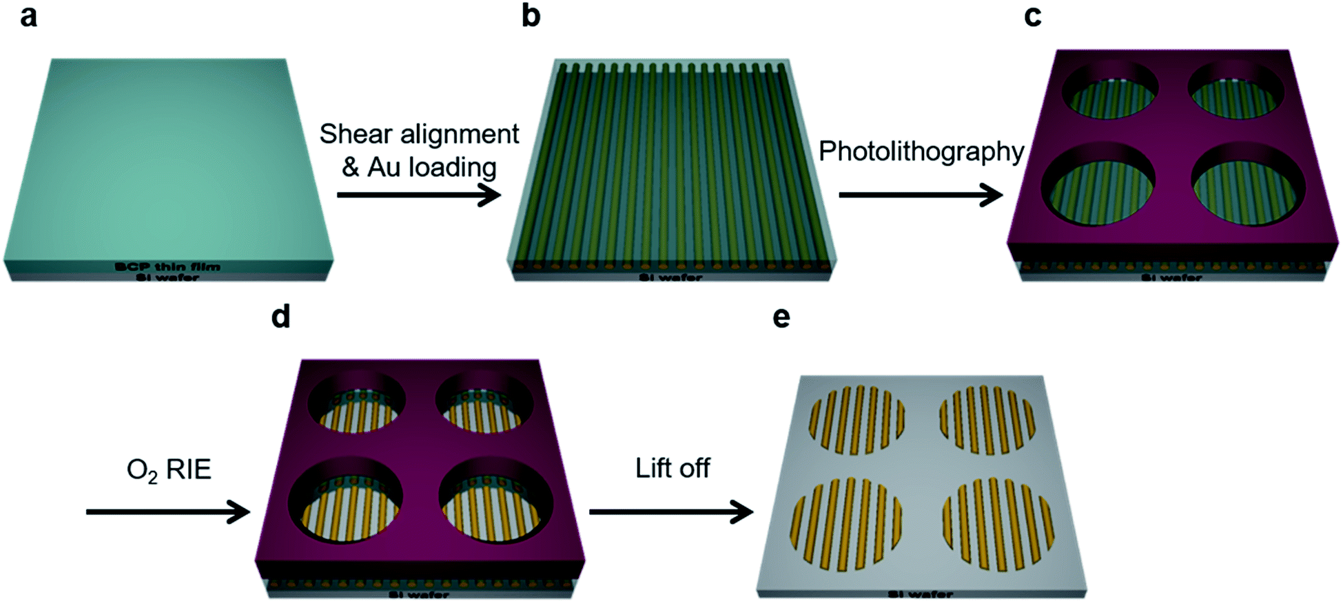 | ||
| Fig. 1 Schematic illustration of overall process for fabrication of Au line patterns in microstructures. (a and b) Shear was applied on BCP thin films and Au ions were loaded. (c) Photolithography process was directly performed on the shear aligned thin films, which created micropatterns on BCP thin films. (d) Followed O2 RIE process and (e) lift-off revealed the aligned nanopatterns in microstructures. | ||
The SEM characterization was readily done after the metal doping because of the enhanced electronic contrast between the PS matrix and the P2VP cylinders. Then, a conventional photolithography technique was applied to the BCP films to fabricate the micropatterns. Two types of PR were used to create microstructures on the surface of the aligned metallic nanopatterns. We found that the positive-tone PR was more reliable for protecting the BCP layer of gold-loaded cylinders. Metal nanopatterns can retain their structures during the photolithography process because of the significantly reduced mobility of the metal-loaded P2VP chains. The subsequent excess O2 RIE revealed the nanostructures in the PR-uncovered area, fixing the Au nanowires onto the substrate. The following lift-off process was done by ultrasonication with toluene, removing the nanopatterns in the PR-covered area, resulting in well-ordered gold nanowires in the selectively micropatterned area.
Film structure and shear alignment of PS-b-P2VP thin films
Firstly, we examined the film structure of the shear-aligned PS-b-P2VP thin films. PS-b-P2VP is known to have an asymmetric wetting condition,44 such that the equilibrium thicknesses at which the uniform films do not terrace are approximately t = (n − 1/2) L0, where t is the film thickness, n is a positive integer, and L0 is the cylinder interlayer spacing. For PS-b-P2VP 44-b-18.5 k, the monolayer thickness t was found to be 57 nm, where no terracing was found after the annealing experiments, as shown in Fig. S1.† Previous studies reported that the quality of the shear alignment can be maximized near the equilibrium thicknesses.19,45,46To find the optimal shearing condition, we systematically varied the film thickness, shearing temperature, and shear stress. The thickness-dependent alignment quality is shown in Fig. S2.† While the cylinders can lie parallel to the shearing direction for a relatively broad range of film thickness, from 30–42 nm, the shear was finally given at 38 nm to ensure a good quality cylinder alignment and at the 58 nm equilibrium thickness.
Fig. 2 confirms that the cylinders parallel to the substrate are nicely aligned along the shearing direction and L0 was found to be 40 nm for both thicknesses. Further film structures were obtained with the ToF-SIMS experiment, which provided depth profiles for the thin films. As shown in Fig. 2a and b, the depth distributions of the PS and P2VP blocks are probed by C6H− and C7H8N− ions, respectively. While the results confirmed the presence of a P2VP wetting layer at the polymer–substrate interface at both thicknesses, hemi-cylinder and full-cylinder structures were found at 38 nm and 58 nm, respectively. The hemi-cylinder structure may not be stable, but can be metastable during the shearing experiments, similar to a previous study.40–42
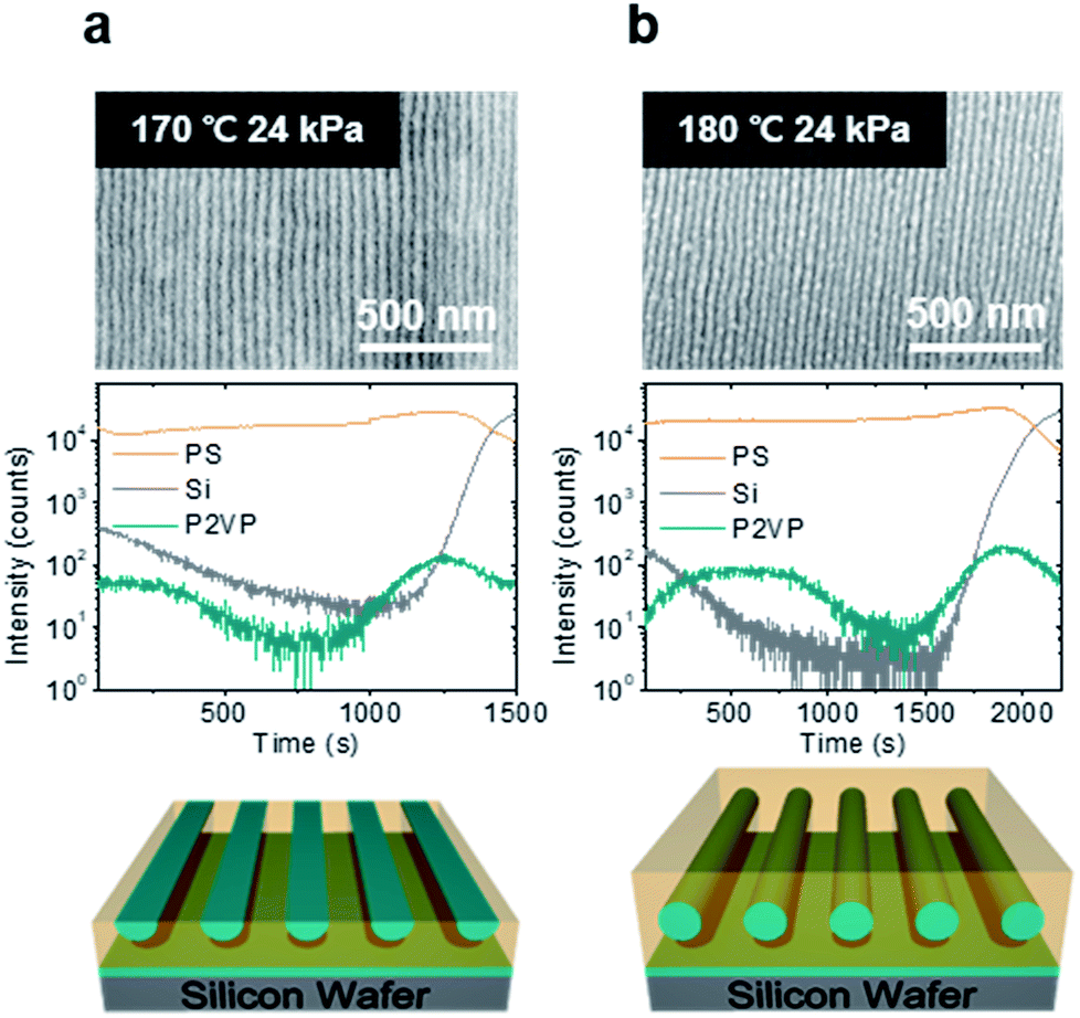 | ||
| Fig. 2 Film structures of shear-aligned thin films at (a) 38 nm and (b) 58 nm. SEM images of shear aligned thin films at both thicknesses are shown in the first row. Tof-SIMS depth profiles are given in the second raw which clearly show that half-cylinders and full-cylinders were obtained at 38 nm and 58 nm thin films, respectively. Suggested film structures for both cases are shown in the third row. | ||
We chose 38 nm as the optimal thickness as this thickness showed the best alignment quality compared to the other thicknesses for the same shearing condition. We further investigated the optimal shearing conditions regarding the temperature and shear stress. In Fig. 3a, the shearing stress increased from 5 kPa to 27 kPa, resulting in an increase of the alignment quality. Comparing the films sheared at temperatures of 150 °C and 170 °C at a given stress (5 kPa), the enhanced alignment quality at a higher temperature confirms that providing sufficient mobility to BCP chains is also important. We calculated Hermans orientation parameters, S to quantify the alignment quality of BCP thin films under each shearing condition.47,48 When S has a value of 1, −0.5 or 0, the cylinders are aligned perfectly parallel, perfectly perpendicular, or randomly to the shearing direction, respectively. The details of calculations were given in the ESI and Fig. S3.† As shown in Fig. 3b, the higher stress and higher temperature were effective to increase the alignment quality; the best condition was chosen to be 170 °C and 24 kPa (S = 0.976).
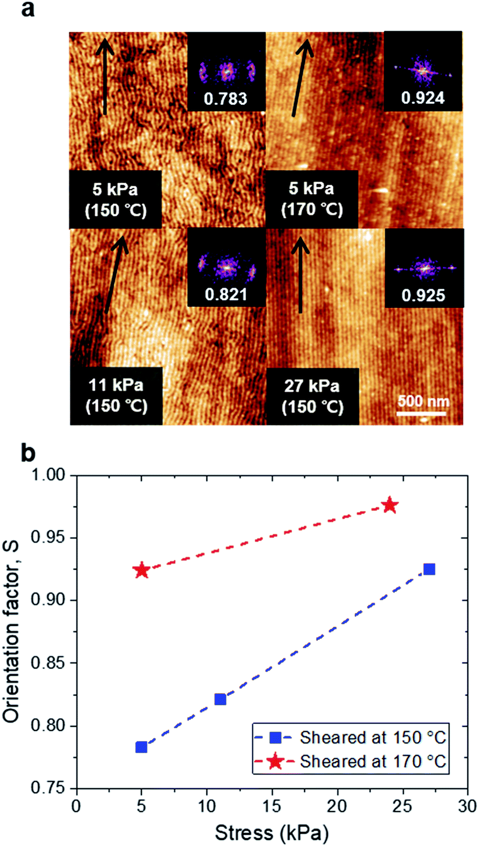 | ||
| Fig. 3 Effect of shearing condition on alignment quality of BCP thin films. (a) AFM height images for shear-aligned thin films with different temperature and stress. FFT images and calculated orientation parameters are shown in the inset of each images. Black arrows indicate the shearing direction. (b) Plot of orientation parameters obtained from each AFM image. | ||
Fabrication of photoresist micro arrays on the aligned BCP films
After shearing, P2VP cylinders were metalized with gold ions; then, micropatterns were created on top of the metalized BCP films, as demonstrated in Fig. 1. A circular-shaped micropattern with a 2.5 μm diameter was employed to demonstrate the proposed hierarchical-structure patterning. Both negative and positive tone PRs were employed, which contain propylene glycol methyl ether acetate (PGMEA) as the solvent. For the negative PR, AZ nLoF was chosen; however, the micropatterns were not clearly developed presumably due to the favorable interaction between the PR and the BCP film, as shown in Fig. S4.† The residual PRs in the developed area disturbed the created nanopatterns. To avoid this problem, Mun et al. employed a graphene oxide layer to avoid direct contact between the BCP thin film and the upper PR layer.49We found that the use of a positive tone PR can successfully create micropatterns directly, without disturbing the alignment of the metal nanowires after lift-off. As shown in Fig. 4a, the photolithography process with a positive-tone PR, AZ5214E, creates sharp and uniform micro arrays on the metal-loaded BCP films. Moreover, we could observe gold nanopatterns in the uncovered regions, which confirms that the development process selectively removed the UV exposed PR layers and did not disturb the underlying BCP patterns (Fig. 4b). The alignment quality was not affected by the PR process as shown in Fig. 4b. The slightly reduced orientation parameter (S = 0.976 → 0.953) may come from some PR residues or rough edges at the boundaries of PRs and BCP layers.
 | ||
| Fig. 4 Developed micro/nano patterns using positive tone PR (AZ5214E) after Au loading in shear-aligned BCP thin films. (a) Low magnification SEM image shows created micro PR patterns after development process. (b) High magnification image clearly shows aligned BCP nanopatterns in uncovered areas. FFT image and calculated orientation parameter are shown in the inset of (b). | ||
We note that both positive and negative PRs contain PGMEA as the solvent. PGMEA has the similar solubility parameter from that of PS and P2VP blocks (16.1 MPa0.5, 18.5 MPa0.5 and 20.4 MPa0.5 for PGMEA, PS and P2VP, respectively). However, the BCP nanopatterns could retain their alignment during the spin casting of PRs because the polymer chain mobility was significantly reduced after metallization. Because both PRs contain the same solvent, the solvent quality difference cannot explain the better result obtained with the positive PRs. We suspect that they have different interaction with BCP layers. The negative PR requires a harsher condition compared to that of positive PRs such as increased baking temperature and time and additional post-baking process, which may create the favorable interaction between BCP and PR layers.
Effect of RIE condition on pattern quality
The etch condition can impact the final quality of the nanowire alignment. After PR development, a subsequent O2 RIE process can reveal the metal nanowires in the PR-uncovered region by removing the PS matrix. Fig. S5b† shows the revealed gold nanowires in the circular-shaped micropatterns after the O2 RIE process. The etch time of the PS matrix for a given etch condition (60 W, 10 mTorr, 10 sccm) was calculated based on the PS homopolymer film-etch rate (65.7 nm min−1) (Fig. S5d†). However, over 1.5 times the etch time for the PS matrix in the BCP was required than that calculated for the PS homopolymers to reveal the metal nanowires.We systematically increased the RIE time at a given pressure to determine how it affected the resulting structures (Fig. 5). Insufficient etching disrupted the nanopatterns after lift-off (sonication in toluene), as shown in Fig. 5 and S5c. Compared to the PS homopolymer etching, a longer etch time was required for removing the PS matrix in the BCP nanowires because the selective etching of the BCPs can be influenced by the nanopatterns, especially in anisotropic etching. To retain the structure of the gold nanowires after RIE, we additionally investigated the effect of the etching power. The gold clusters that often formed during RIE could be prevented when the RIE power was increased (Fig. S6a†), thus enhancing the structural quality of the resulting patterns.
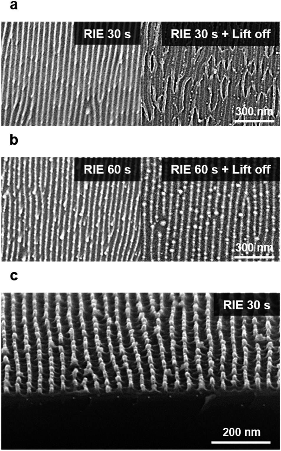 | ||
| Fig. 5 SEM images of Au line patterns after RIE process at 60 W, 10 mTorr, 10 sccm for (a) 30 s and (b) 60 s. The right side images of (a) and (b) show their structures after lift-off with sonication in toluene for 15 min. (c) The cross-sectional SEM image of the left in (a) revealing polymeric residues between the lines. | ||
We also analyzed the quality of produced gold patterns by performing XPS measurements. We confirmed that the presence of Au3+ ions at the metal loading step (Fig. S6b-a†), and they were completely reduced to Au0 after RIE (Fig. S6b-b†). The peak position of 4f7/2 is comparable to that of standard gold (84 eV) and further optimization could be achieved by additional annealing process.50
Obtaining final structures with lift-off process
The RIE process removed the residual polymers in the PR-uncovered region, and a subsequent lift-off removed the PR residue, leaving the nanowires in the micropatterns. The lift-off for PR can be done by ultrasonication with toluene. The films were immersed in toluene at room temperature with occasional sonication for 15 min. Fig. 6b shows the aligned metal wires in the circular-shaped micropatterns. The nicely aligned gold nanowires in the shaped micropatterns were fabricated in 1.2 × 1.2 cm2 areas. | ||
| Fig. 6 Obtained final structures after overall process. (a) Low magnification SEM image shows that the microstructures created from the lithography process were transferred to Au line patterns. (b) High magnification SEM image from bright region shows that aligned Au line patterns. 2D FFT is shown in the inset with orientation parameter. See ESI.† | ||
Quantification of produced final structures
The alignment quality of the final structure was quantified with the calculation of orientation parameters. The orientation parameter was 0.922, confirming the good alignment quality of the nanowires. Further analysis for the micropatterns was performed with image analysis (Fig. S7†). The obtained circular micropatterns have critical dimension (CD) of 2308.54 ± 10.78 nm, contact width roughness (CWR) of 141.81 ± 9.79 nm, and contact edge roughness (CER) of 84.54 ± 5.63 nm. The CD value of obtained micropatterns was close to that of photomask patterns (2.5 μm), implying a successful transfer of PR patterns.We also analyzed the structure quality of nanopatterns. The CD, line width roughness (LWR), and line edge roughness (LER) of nanopatterns in the circular micropattern were 6.8 ± 0.12 nm, 4.92 ± 0.34 nm, and 2.39 ± 0.16 nm, respectively. Further optimization of RIE process would increase the transferred pattern quality.
Conclusion
In this study, we demonstrated the fabrication of metal nanowires in the designed micropatterned areas with a combination of shear-aligned block copolymer films and a photolithographic technique. The proposed method did not require an additional pattern transfer or sacrificial layer, but employed direct photolithography, simplifying the entire fabrication process. Moreover, aligned nanowires in large areas with a long-range order were readily fabricated. The quality of aligned structures was evaluated by several parameters, showing a good quality of micro- and nano- patterns. Further optimization in fabrication conditions for better quality of nanopatterns remains as future work. We believe the proposed method can be widely employed in various BCP mediated nanopatterning areas, increasing the versatility of nanopatterns.Conflicts of interest
There are no conflicts to declare.Acknowledgements
This work was supported by the Basic Science Research Program through the National Research Foundation of Korea (NRF) funded by Ministry of Education (NRF-2017R1D1A1B03030925) and by the year of 2015 Research Fund of the Ulsan National Institute of Science and Technology (UNIST) (1.150111.01).References
- D. O. Shin, J.-R. Jeong, T. H. Han, C. M. Koo, H.-J. Park, Y. T. Lim and S. O. Kim, J. Mater. Chem., 2010, 20, 7241–7247 RSC.
- C. K. Jeong, H. M. Jin, J. H. Ahn, T. J. Park, H. G. Yoo, M. Koo, Y. K. Choi, S. O. Kim and K. J. Lee, Small, 2014, 10, 337–343 CrossRef PubMed.
- Y. Kang, J. J. Walish, T. Gorishnyy and E. L. Thomas, Nat. Mater., 2007, 6, 957 CrossRef PubMed.
- D. P. Song, C. Li, N. S. Colella, X. Lu, J. H. Lee and J. J. Watkins, Adv. Opt. Mater., 2015, 3, 1169–1175 CrossRef.
- B. R. Sveinbjörnsson, R. A. Weitekamp, G. M. Miyake, Y. Xia, H. A. Atwater and R. H. Grubbs, Proc. Natl. Acad. Sci. U. S. A., 2012, 109, 14332–14336 CrossRef PubMed.
- A. M. Urbas, M. Maldovan, P. DeRege and E. L. Thomas, Adv. Mater., 2002, 14, 1850–1853 CrossRef.
- S. K. Cha, J. H. Mun, T. Chang, S. Y. Kim, J. Y. Kim, H. M. Jin, J. Y. Lee, J. Shin, K. H. Kim and S. O. Kim, ACS Nano, 2015, 9, 5536–5543 CrossRef PubMed.
- P. A. Mistark, S. Park, S. E. Yalcin, D. H. Lee, O. Yavuzcetin, M. T. Tuominen, T. P. Russell and M. Achermann, ACS Nano, 2009, 3, 3987–3992 CrossRef PubMed.
- K. Zhang, L. Zhang, F. L. Yap, P. Song, C. W. Qiu and K. P. Loh, Small, 2016, 12, 1302–1308 CrossRef PubMed.
- C. Black, Appl. Phys. Lett., 2005, 87, 163116 CrossRef.
- J. G. Son, M. Son, K. J. Moon, B. H. Lee, J. M. Myoung, M. S. Strano, M. H. Ham and C. A. Ross, Adv. Mater., 2013, 25, 4723–4728 CrossRef PubMed.
- X. Yu, K. Xiao, J. Chen, N. V. Lavrik, K. Hong, B. G. Sumpter and D. B. Geohegan, ACS Nano, 2011, 5, 3559–3567 CrossRef PubMed.
- E. J. Crossland, M. Kamperman, M. Nedelcu, C. Ducati, U. Wiesner, D.-M. Smilgies, G. E. Toombes, M. A. Hillmyer, S. Ludwigs and U. Steiner, Nano Lett., 2008, 9, 2807–2812 CrossRef PubMed.
- P. Docampo, S. Guldin, M. Stefik, P. Tiwana, M. C. Orilall, S. Hüttner, H. Sai, U. Wiesner, U. Steiner and H. J. Snaith, Adv. Funct. Mater., 2010, 20, 1787–1796 CrossRef.
- C. K. Jeong, K. M. Baek, S. Niu, T. W. Nam, Y. H. Hur, D. Y. Park, G.-T. Hwang, M. Byun, Z. L. Wang and Y. S. Jung, Nano Lett., 2014, 14, 7031–7038 CrossRef PubMed.
- I. Bita, J. K. Yang, Y. S. Jung, C. A. Ross, E. L. Thomas and K. K. Berggren, Science, 2008, 321, 939–943 CrossRef PubMed.
- S. O. Kim, H. H. Solak, M. P. Stoykovich and N. J. Ferrier, Nature, 2003, 424, 411 CrossRef PubMed.
- C.-C. Liu, A. Ramírez-Hernández, E. Han, G. S. Craig, Y. Tada, H. Yoshida, H. Kang, S. Ji, P. Gopalan and J. J. de Pablo, Macromolecules, 2013, 46, 1415–1424 CrossRef.
- D. E. Angelescu, J. H. Waller, D. H. Adamson, P. Deshpande, S. Y. Chou, R. A. Register and P. M. Chaikin, Adv. Mater., 2004, 16, 1736–1740 CrossRef.
- Z. Qiang, Y. Zhang, J. A. Groff, K. A. Cavicchi and B. D. Vogt, Soft Matter, 2014, 10, 6068–6076 RSC.
- P. W. Majewski, A. Rahman, C. T. Black and K. G. Yager, Nat. Commun., 2015, 6, 7448 CrossRef PubMed.
- A. Keller, E. Pedemonte and F. Willmouth, Nature, 1970, 225, 538–539 CrossRef PubMed.
- R. Glass, M. Möller and J. P. Spatz, Nanotechnology, 2003, 14, 1153 CrossRef.
- B. Gorzolnik, P. Mela and M. Moeller, Nanotechnology, 2006, 17, 5027 CrossRef.
- P. Liu, J. Sun, J. Huang, R. Peng, J. Tang and J. Ding, Nanoscale, 2010, 2, 122–127 RSC.
- Y. Liu, H. Hu, W. Ye, F. Zhou and J. Hao, J. Mater. Chem. C, 2013, 1, 902–907 RSC.
- T. Chang, B. Du, H. Huang and T. He, ACS Appl. Mater. Interfaces, 2016, 8, 22705–22713 Search PubMed.
- S.-J. Jeong, J. E. Kim, H.-S. Moon, B. H. Kim, S. M. Kim, J. B. Kim and S. O. Kim, Nano Lett., 2009, 9, 2300–2305 CrossRef PubMed.
- E. Han, H. Kang, C. C. Liu, P. F. Nealey and P. Gopalan, Adv. Mater., 2010, 22, 4325–4329 CrossRef PubMed.
- S. Nagarajan, T. P. Russell and J. J. Watkins, Adv. Funct. Mater., 2009, 19, 2728–2734 CrossRef.
- A. P. Lane, M. J. Maher, C. G. Willson and C. J. Ellison, ACS Macro Lett., 2016, 5, 460–465 CrossRef.
- V. K. Daga, E. L. Schwartz, C. M. Chandler, J.-K. Lee, Y. Lin, C. K. Ober and J. J. Watkins, Nano Lett., 2011, 11, 1153–1160 CrossRef PubMed.
- M. S. Onses, C. Song, L. Williamson, E. Sutanto, P. M. Ferreira, A. G. Alleyne, P. F. Nealey, H. Ahn and J. A. Rogers, Nat. Nanotechnol., 2013, 8, 667–675 CrossRef PubMed.
- R. Kane, R. Cohen and R. Silbey, Chem. Mater., 1996, 8, 1919–1924 CrossRef.
- J. Ciebien, R. Clay, B. Sohn and R. Cohen, New J. Chem., 1998, 22, 685–691 RSC.
- Y.-H. La, M. P. Stoykovich, S.-M. Park and P. F. Nealey, Chem. Mater., 2007, 19, 4538–4544 CrossRef.
- Y. Saito, T. Higuchi, H. Jinnai, M. Hara, S. Nagano, Y. Matsuo and H. Yabu, Macromol. Chem. Phys., 2016, 217, 726–734 CrossRef.
- H. Yabu and S. Nagano, RSC Adv., 2017, 7, 33086–33090 RSC.
- J. Chai and J. M. Buriak, ACS Nano, 2008, 2, 489–501 CrossRef PubMed.
- S. Y. Kim, A. Nunns, J. Gwyther, R. L. Davis, I. Manners, P. M. Chaikin and R. A. Register, Nano Lett., 2014, 14, 5698–5705 CrossRef PubMed.
- Y. C. Kim, D. H. Kim, S. H. Joo, N. K. Kwon, T. J. Shin, R. A. Register, S. K. Kwak and S. Y. Kim, Macromolecules, 2017, 50, 3607–3616 CrossRef.
- S. Y. Kim, J. Gwyther, I. Manners, P. M. Chaikin and R. A. Register, Adv. Mater., 2014, 26, 791–795 CrossRef PubMed.
- J. Chai, D. Wang, X. Fan and J. M. Buriak, Nat. Nanotechnol., 2007, 2, 500–506 CrossRef PubMed.
- P. Grim, I. Nyrkova, A. Semenov, G. Ten Brinke and G. Hadziioannou, Macromolecules, 1995, 28, 7501–7513 CrossRef.
- R. L. Davis, P. M. Chaikin and R. A. Register, Macromolecules, 2014, 47, 5277–5285 CrossRef.
- R. L. Davis, B. T. Michal, P. M. Chaikin and R. A. Register, Macromolecules, 2015, 48, 5339–5347 CrossRef.
- K. J. Choi, J. E. Spruiell and J. L. White, J. Polym. Sci., Polym. Lett. Ed., 1982, 20, 27–47 CrossRef.
- P. W. Majewski and K. G. Yager, J. Phys.: Condens. Matter, 2016, 28, 403002 CrossRef PubMed.
- J. H. Mun, S. K. Cha, Y. C. Kim, T. Yun, Y. J. Choi, H. M. Jin, J. E. Lee, H. U. Jeon, S. Y. Kim and S. O. Kim, Small, 2017, 13, 1603939 CrossRef PubMed.
- K. C. Kwon, B. J. Kim, J.-L. Lee and S. Y. Kim, J. Mater. Chem. C, 2013, 1, 2463–2469 RSC.
Footnote |
| † Electronic supplementary information (ESI) available. See DOI: 10.1039/c8ra02273a |
| This journal is © The Royal Society of Chemistry 2018 |