
 Open Access Article
 This Open Access Article is licensed under a Creative Commons Attribution-Non Commercial 3.0 Unported Licence
High-performance organic circuits based on precisely aligned single-crystal arrays
Jingu Kang a,
Minwook Leea,
Antonio Facchettibc,
Jaekyun Kim*d and
Sung Kyu Park*a
a,
Minwook Leea,
Antonio Facchettibc,
Jaekyun Kim*d and
Sung Kyu Park*a
aSchool of Electrical and Electronic Engineering, Chung-Ang University, Seoul, 06974, Republic of Korea. E-mail: skpark@cau.ac.kr
bDepartment of Chemistry, The Materials Research Center, The Argonne-Northwestern Solar Energy Research Center, Northwestern University, Evanston, Illinois 60208, USA
cFlexterra Inc., Skokie, Illinois 60077, USA
dDepartment of Photonics and Nanoelectronics, Hanyang University, Ansan, Gyeonggi-do 15588, Republic of Korea. E-mail: jaekyunkim@hanyang.ac.kr
First published on 11th May 2018
Abstract
In this paper, we demonstrate high-performance organic logic circuits based on precisely controlled organic single-crystal arrays. Well-aligned microrod shaped 2,7-dioctyl[1]benzothieno[3,2-b][1]benzothiophene (C8-BTBT) single-crystal organic thin-film-transistors (OTFTs) were fabricated via solvent mediated molecular tailoring with a polymeric sacrificial layer, exhibiting saturation mobility of >2 cm2 V−1 s−1. Using this approach, precise placement of organic crystal arrays in a controlled orientation was successfully achieved, enabling the fabrication of OTFT-based inverter circuits with a gain of 1.37 (V V−1). Furthermore, it was demonstrated that, by varying the number of single-crystal microrods, the device dimension and corresponding circuit performance can be modulated. A high-performance inverter operation with various interdigitating single-crystal microrod arrays can thus be achieved.
Introduction
Noteworthy progress in organic electronics has been made to satisfy various demands such as precise patterning, high-performance, and organic circuit applications, in order to realize next generation displays and electronics.1–3 Moreover, the solution processing of organic semiconductors has been considered a promising candidate for large-scale fabrication at low temperatures and at relatively low cost. This has ensured its widespread application in electrical circuits.4,5 Accordingly, it has been reported that solution-processed organic thin film transistors (OTFTs) and various OTFT-based circuits continue to improve device properties, including mobility and maximum gain, which ensures a functionality on par with their inorganic counterparts.6,7 Given that solution processing is a promising candidate for high-performance organic electronics, the formation and molecular properties of single crystalline structures are being actively investigated, primarily because of their efficient charge transport properties and environmental stability.4,8,9TIPS-pentacene is widely studied and employed as an organic material for single crystal formation and charge transport within its molecular structure.10 In addition, single crystal phases formed from polycrystalline films through the reorganization of organic molecules under solvent-ambient environments have been reported as contributing to improvement in device performance.11 Electrical characteristics of OSC-based TFTs have thus noticeably improved, which promotes interest toward diverse OSC-based circuit applications.3,12,13 For instance, a complementary inverter based on p- and n-type OTFTs was fabricated using the droplet-pinned crystallization (DPC) method for single crystallization. It showed excellent voltage transfer characteristics with a high gain of 155 (V V−1).3
Although considerable efforts have been made in the development of single crystal growth methodologies and theoretical investigation of the charge transport phenomenon, fabrication and relevant simulation of OSC-based circuits with varying device dimensions is a relatively unexplored area.14–17 Well-defined device dimensions are highly important in circuit application, since circuit performance parameters such as gain can be adjusted by changing both the geometry and the electrical properties of active devices.
Reorganization of organic molecules under a solvent-rich environment is a promising technology because it can easily be translated into large-area OSC fabrication. In addition, by utilizing a surface-modified polymer sacrificial layer, spatially controllable 2,7-dioctyl[1]benzothieno[3,2-b][1]benzothiophene (C8-BTBT) OSCs can be positioned on a substrate for subsequent device fabrication in a scalable manner. Therefore, our developed method can be employed to fabricate high-performance OSC-based circuits and evaluate their operation with an assistance of a circuit simulator.
In this article, we fabricated a C8-BTBT OSC-based inverter composed of a driver and loader whose effective channel dimensions were quantitatively defined by the photochemical molecular tailoring of PMMA and subsequent vapor annealing. OSC arrays and their corresponding devices were successfully fabricated at the desired locations, thereby resulting in high mobility and large drain current. Consequently, we demonstrated that our quantitative modulation of OSCs is significantly effective in tuning the voltage transfer characteristic (VTC) of the OSC inverter and that the configuration of circuit geometry is consistent with simulation results.
Experimental
For the fabrication of microrod-OSC TFTs and inverter circuits, borosilicate glass (Eagle 2000, JMC glass) was used as the substrate. For gate electrodes, 5 nm of chrome and 35 nm of gold were thermally deposited onto the glass substrate and patterned using a conventional photolithography process. A 100 nm-layer of aluminum oxide was formed as the gate dielectric using the atomic layer deposition (ALD) technique. Then, the polymeric sacrificial layer (poly(methyl methacrylate), PMMA, A4 950, MicroChem) was spun and annealed at 180 °C for 20 min. For photochemical patterning of the sacrificial layer, we carried out deep-UV irradiation from a low-pressure mercury lamp (LPML, main peak of 254 nm with 90% and 185 nm with 10%) onto the PMMA layer using a quartz photomask under nitrogen purging for 30 min. In this step, the side chains of the DUV-exposed regions of the PMMA layer underwent dissociation and cross-links were formed between the backbones and neighboring molecules. This resulted in reduced solubility to the solvent vapor and diffusivity of organic molecules relative to pristine PMMA. The fabrication of selective patterning in the PMMA layer has been schematically depicted in Fig. 1(a).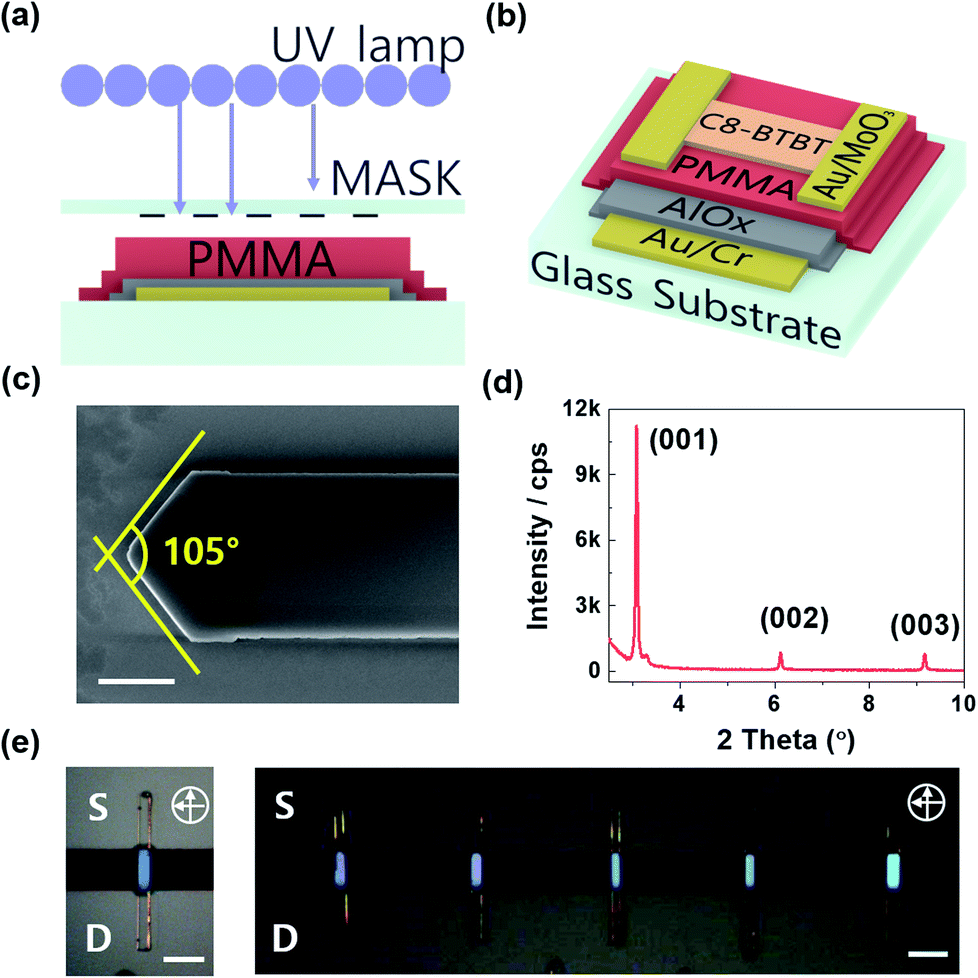 | ||
| Fig. 1 Schematics of (a) DUV-irradiation process under nitrogen purging and (b) a single-microrod device structure. (c) FE-SEM image of one side of the microrod-OSC. The scale bar represents 3 μm. (d) XRD spectrum of the OSC arrays. (e) CPOM images of the microrod-OSC devices for single (left) and quintuple (right) arrays. White scale bars represent 20 μm. | ||
A 0.5 wt% of C8-BTBT solution was prepared by dissolving the powder in chlorobenzene followed by spinning of the solution onto the pre-patterned PMMA layer at 3000 rpm for 20 s. Selective single crystalline formation in a microrod structure and the spatial control of arrays were achieved using the solvent vapor annealing (SVA) process. The FE-SEM image and X-ray diffraction (XRD) spectrum were obtained using SIGMA (Carl Zeiss) and D8-Advance (Bruker-ASX) instruments, respectively. For the source and drain electrodes, 5 nm of molybdenum trioxide (MoO3) and 50 nm of gold were sequentially deposited. The final device structure for a single-microrod is schematically depicted in Fig. 1(b). The electrical properties of the devices and circuits were measured in a dark box at room temperature using a semiconductor parameter analyzer (4156C, Agilent). The serial capacitance of PMMA/Al2O3 was 24.35 nF cm−2. The width and length of the OSC were measured by optical microscopy.
Results and discussion
The VTC of an inverter depends on the properties of the drive and load transistor, such as device dimensions and electrical characteristics, which consequently affect the maximum gain of the circuit. In order to validate the tunability of the channel dimension by the quantitative modulation of OSC arrays, we fabricated OSC TFTs based on single-microrod crystal arrays. As reported in our previous study, multi-aligned OSC arrays can be easily fabricated by the photochemical molecular tailoring method described previously.18 Using this technique, single crystalline microrod arrays of C8-BTBT were successfully obtained in a predefined area. To identify the molecular structure and single crystal phase of OSC arrays, we carried out FE-SEM and XRD analysis as shown in Fig. 1(c) and (d), respectively. The FE-SEM image clearly reveals that the top surface of the microrod OSC is planar and the facet angle of the growth direction is 105°. The narrow peaks of the XRD spectrum also suggest a high degree of crystallinity in the microrod OSC arrays, which is consistent with the molecular structure observed in previous studies.11,18 In addition, we analyzed cross-polarized optical microscopy (CPOM) images, in which bright color in the OSC region typically corresponds to high crystallinity. The results can be seen in Fig. 1(e).We found that the effective channel width and length are 5 μm and 20 μm, respectively for single-microrod TFT, and 25 μm and 20 μm, respectively for quadrupled OSC array TFTs. Since OSCs are completely isolated from each other and from adjacent devices, the ability to selectively configure OSCs is advantageous in preventing crosstalk between neighboring devices. This offers a profitable approach to appropriate operation and excellent performance of organic circuits.
Fig. 2(a) and (b) show the representative transfer characteristics of microrod-OSC TFTs. Although both devices have shown almost identical field-effect saturation mobilities of 2.91 cm2 V−1 s−1 for the single OSC and 2.77 cm2 V−1 s−1 for the quintuple OSC array (the linear mobility is 1.36 cm2 V−1 s−1 for the single and 1.18 cm2 V−1 s−1 for the quintuple at VD = −10 V), the drain currents dramatically increased (by almost 5-fold) when the channel width throughout the precisely controlled multi-rod arrangement was increased. Despite the fact that the devices generally suffer from relatively high contact resistance (verified by output characteristics reported in previous studies) possibly due to the large thickness of C8-BTBT OSC (approximately 200 nm) and our top-contact device structure, the tunable drain current and high saturation mobility make this device a promising building block for logic circuit application.
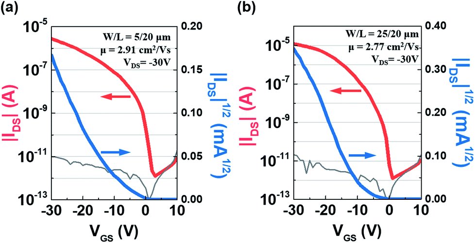 | ||
| Fig. 2 Transfer characteristics of (a) the single-microrod device and (b) the quadrupled OSC array device. The gray solid line represents leakage current. The on-state current values at VGS = −30 V are (a) 2.7 μA and (b) 12.1 μA. | ||
Fig. 3(a) shows a schematic diagram of a microrod-OSC inverter, which includes multi-aligned p-type microrod-OSC TFTs for the loader and driver. To configure the enhancement load of the inverter, the gate electrode was connected to the supply voltage (VDD). High maximum gain of an inverter can be achieved by modulating the ratio of channel width to length for the loader and driver TFTs. The loader was designed to exhibit a higher aspect channel ratio than the driver. As mentioned above, the number of multi-aligned OSCs can be quantitatively modulated for single and quintuple microrod arrays. Also, the length of microrod-OSCs can easily be varied by photochemical patterning of the sacrificial layer. For example, in this study, OSC arrays were produced at predefined locations, with a 200 μm-long microrod-OSC array for the 100 μm-long loader channel and a 100 μm-long microrod-OSC array for the 20 μm-long driver channel. As a result, the effective device dimensions of the loader (TL) and the driver (TD) were readily controlled (W = 5 μm and L = 100 μm for the loader, W = 15 μm and L = 20 μm for the driver). Fig. 3(b) shows the CPOM image of the fabricated inverter with microrod-OSC arrays.
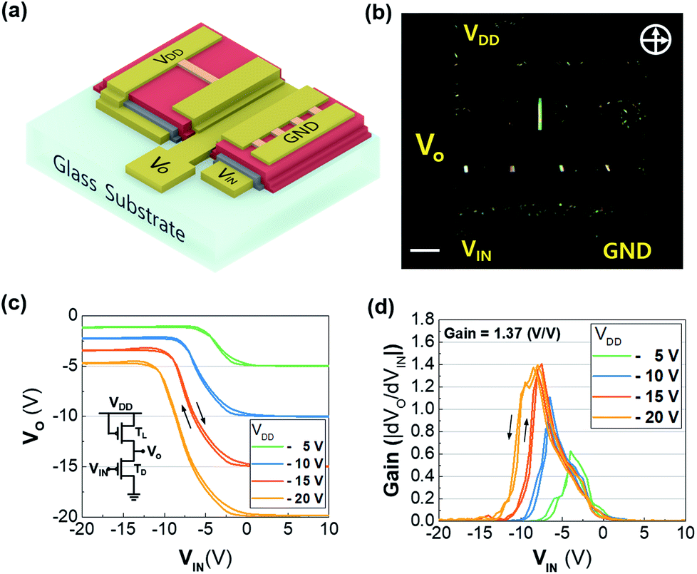 | ||
| Fig. 3 (a) Schematic of a microrod-OSC inverter structure. (b) CPOM image of a microrod-OSC inverter. Bright regions depict OSC arrays. White scale bar represents 100 μm. (c) Voltage transfer characteristics for each supply voltage and (d) gain curve for a microrod-OSC inverter. | ||
Fig. 3(c) depicts the voltage transfer characteristic (VTC) of the microrod-OSC inverter. The input voltage ranged between −20 and +20 V while VDD of −5, −10, −15, and −20 V were used. VO is diminished to VDD - VTH because the enhancement mode OTFT was used as the loader for the inverter. However, the noise margin of the VTC is large enough for logical operations at each value of VDD owing to the high aspect ratios (kD/kL) of TD and TL. Also, the inverter shows nearly negligible hysteresis. As a result, a maximum gain of 1.37 (V V−1), defined as |dVO/dVIN|, was obtained at a VDD of −20 V as shown in Fig. 3(d), which is quite a high gain for an enhancement load.
In order to investigate the feasibility of device dimension manipulation, we quantitatively modulated the channel width of TL by controlling the number of aligned microrod-OSCs. The VTC of the inverter for an enhancement load is mainly defined by the effective resistance, which is related to the width-to-length ratio of the TL. First, we conducted a simulation study of TL channel width modulation. In our microrod-OSC inverter, the width of the single-microrod-OSC is around 5 μm. We initially set 15 μm as the effective channel width of TL (with a triple microrod-OSCs array), and then reduced it to 5 μm, which resulted in an increase in aspect ratio (kD/kL) from 6.6 to 20.0. As shown in Fig. 4(a), the increase in gain was observed in the simulation, along with a decrease in TL channel width from 1.25 to 1.47 μm. In the case of our microrod-OSC inverter, as we expected, VTC was tuned and gain increased from 1.31 to 1.86 when the number of aligned OSCs was varied, as shown in Fig. 4(b). This result agrees well with our simulation result. Therefore, we can retain the logical inverting operation in the almost full swing range, securing higher gain by quantitative modulation of inverter geometry. Our results indicate that the number of OSCs can be readily manipulated using simple surface tailoring methodology, which provides high electrical performance in organic circuit applications.
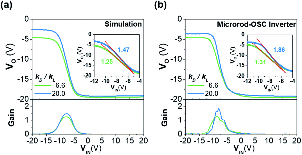 | ||
| Fig. 4 VTC and gain curves of (a) a simulation and (b) a microrod-OSC inverter. The legends given in (a) and (b) represent aspect ratio (kD/kL), which is varied by modulation of TL channel. When the TL width decreases, aspect ratio increases. The maximum gains ranged between 1.25 and 1.47 in (a) and between 1.31 and 1.86 in (b). The insets of (a) and (b) are scaled up from −12 V to −4 V on the X-axis. | ||
Conclusions
C8-BTBT microrod-OSC arrays were precisely manipulated at the desired locations by the spatial photochemical modification of polymeric sacrificial layers and subsequent solvent vapor annealing. Based on the experimental results, high-performance organic TFTs can be fabricated using a controllable alignment of OSC arrays. Moreover, we successfully implemented simple logic circuits using the multi-aligned microrod-OSC arrays for load and drive TFTs. The inverter circuits with enhancement load demonstrated excellent switching operation, with gain more than 1 (V V−1) by the successful loading of 200 μm-long microrod-OSCs in the TL channel and 4-fold of 100 μm-long microrod-OSC arrays for the TD channel. Therefore, we believe that the precise control of high-performance OSCs in the desired area will offer greater tunability in organic circuit design, enabling their wider utilization in high-performance organic electronics.Conflicts of interest
There are no conflicts to declare.Acknowledgements
This research was partially supported by the Chung-Ang University Research Grants in 2017, by the Human Resources Development (No. 20174030201810) of the Korea Institute of Energy Technology Evaluation and Planning (KETEP) grant funded by the Korea government Ministry of Trade, Industry and Energy, and by the Engineering Research Center of Excellence (ERC) Program supported by National Research Foundation (NRF), Korean Ministry of Science & ICT (MSIT) (Grant No. NRF-2017R1A5A1014708).References
- T. Minari, C. Liu, M. Kano and K. Tsukagoshi, Adv. Mater., 2012, 24, 299–306 CrossRef CAS PubMed
.
- W. Deng, X. Zhang, L. Wang, J. Wang, Q. Shang, X. Zhang, L. Huang and J. Jie, Adv. Mater., 2015, 27, 7305–7312 CrossRef CAS PubMed
- H. Li, B. C. K. Tee, G. Giri, J. W. Chung, S. Y. Lee and Z. Bao, Adv. Mater., 2012, 24, 2588–2591 CrossRef CAS PubMed
- Y. Yuan, G. Giri, A. L. Ayzner, A. P. Zoombelt, S. C. B. Mannsfeld, J. Chen, D. Nordlund, M. F. Toney, J. Huang and Z. Bao, Nat. Commun., 2014, 5, 3005 Search PubMed
- F. G. Del Pozo, S. Fabiano, R. Pfattner, S. Georgakopoulos, S. Galindo, X. Liu, S. Braun, M. Fahlman, J. Veciana, C. Rovira, X. Crispin, M. Berggren and M. Mas-Torrent, Adv. Funct. Mater., 2016, 26, 2379–2386 CrossRef CAS
- M. Grundmann, H. Frenzel, A. Lajn, M. Lorenz, F. Schein and H. Von Wenckstern, Phys. Status Solidi A, 2010, 207, 1437–1449 CrossRef CAS
- H. Frenzel, F. Schein, A. Lajn, H. von Wenckstern and M. Grundmann, Appl. Phys. Lett., 2010, 96, 113502 CrossRef
- J. Chang, C. Chi, J. Zhang and J. Wu, Adv. Mater., 2013, 25, 6442–6447 CrossRef CAS PubMed
- Y. Diao, B. C.-K. Tee, G. Giri, J. Xu, D. H. Kim, H. a Becerril, R. M. Stoltenberg, T. H. Lee, G. Xue, S. C. B. Mannsfeld and Z. Bao, Nat. Mater., 2013, 12, 665–671 CrossRef CAS PubMed
- G. Giri, E. Verploegen, S. C. Mannsfeld, S. Atahan-Evrenk, H. Kim do, S. Y. Lee, H. A. Becerril, A. Aspuru-Guzik, M. F. Toney and Z. Bao, Nature, 2011, 480, 504 CrossRef CAS PubMed
- C. Liu, T. Minari, X. Lu, A. Kumatani, K. Takimiya and K. Tsukagoshi, Adv. Mater., 2011, 23, 523–526 CrossRef CAS PubMed
- Y. Li, D. Ji, J. Liu, Y. Yao, X. Fu, W. Zhu, C. Xu, H. Dong, J. Li and W. Hu, Sci. Rep., 2015, 5, 13195 CrossRef CAS PubMed
- X. Zhao, Y. Tong, Q. Tang and Y. Liu, Adv. Electron. Mater., 2015, 1, 1500239 CrossRef
- H. Xu, Y. C. Zhou, X. Y. Zhou, K. Liu, L. Y. Cao, Y. Ai, Z. P. Fan and H. L. Zhang, Adv. Funct. Mater., 2014, 24, 2907–2915 CrossRef CAS
- Y. Wu, J. Feng, X. Jiang, Z. Zhang, X. Wang, B. Su and L. Jiang, Nat. Commun., 2015, 6, 6737 CrossRef CAS PubMed
- Y. Wu, J. Feng, B. Su and L. Jiang, Adv. Mater., 2016, 28, 2266–2273 CrossRef CAS PubMed
- J. Feng, X. Jiang, X. Yan, Y. Wu, B. Su, H. Fu, J. Yao and L. Jiang, Adv. Mater., 2017, 29, 1603652 CrossRef PubMed
- J. Kang, J. Kim, J. W. Jo, J. S. Heo, M. G. Kim, Y. H. Kim, J. Kim and S. K. Park, Small, 2016, 1602467, 1–10 Search PubMed
| This journal is © The Royal Society of Chemistry 2018 |