
 Open Access Article
 This Open Access Article is licensed under a Creative Commons Attribution-Non Commercial 3.0 Unported Licence
Bio-inspired semi-transparent silver nanowire conductor based on a vein network with excellent electromechanical and photothermal properties†
You-Xia Qiangabc,
Chun-Hua Zhu *a,
Ye-Ping Wua,
Sheng Cuibc and
Yu Liu*a
*a,
Ye-Ping Wua,
Sheng Cuibc and
Yu Liu*a
aInstitute of Chemical Materials, China Academy of Engineering Physics, Mianyang, Sichuan 621900, China. E-mail: chzhu@caep.cn; liuyu307@caep.cn; Fax: +86-816-2486342
bCollege of Materials Science and Engineering, Nanjing Tech University, Nanjing 210009, PR China
cJiangsu Collaborative Innovation Center for Advanced Inorganic Function Composites, Nanjing Tech University, Nanjing 210009, PR China
First published on 26th June 2018
Abstract
A bio-inspired conductive binary-network of vein–silver nanowires (AgNWs) was embedded in poly(dimethylsiloxane) (PDMS) to prepare a semi-transparent stretchable conductor (vein–AgNWs–PDMS) by a simple dipping process. The special conductive structure was constructed by using veins with a porous structure as an ideal skeleton to load AgNW networks, which allowed the vein–AgNWs–PDMS composite to show a low sheet resistance of 1 Ω sq−1 with 74% transmittance. The figure of merit of vein–AgNWs–PDMS is as high as 2502 and can be adjusted easily by controlling the times of the dipping cycle. Furthermore, the vein–AgNWs–PDMS conductor can retain high conductivity after 150% mechanical elongation and exhibit excellent electromechanical stability in repeated stretch/release tests with 60% strain (500 cycles). As an example of an application, patterned light-emitting diode (LED) arrays using the vein–AgNWs–PDMS conductors have been fabricated, and worked well under deformation. Moreover, the photo-thermal properties of the vein–AgNWs–PDMS composite have been demonstrated by a position heating experiment using near-infrared (NIR) laser irradiation and the generated heat can be effectively dissipated through the vein network to avoid local overheating. Due to the high-performance and facile fabrication process, the vein–AgNWs–PDMS conductors will have multifunctional applications in stretchable electronic devices.
1. Introduction
Stretchable transparent conductors (STCs) have attracted much attention in recent years. Compared with conventional inherent brittle oxide-based electronics, STCs can retain high optical transmission and excellent electrical conductivity under large bending and stretching, which plays an essential role in transparent stretchable electronic devices such as electronic skin, photovoltaic devices, display and organic light-emitting diodes.1–5Such STCs have been developed by combining conducting materials such as metal nanowires/nanoparticles, carbon nanotubes and graphene with transparent stretchable substrates.6–12 However, most STCs prepared by this method have a significant reduction in conductivity under deformation.13–18 For example, Akter et al. prepared a STC with a low sheet resistance of 35 Ω sq−1 that exhibited 80% transmittance through depositing silver nanowires (AgNWs) on a polydopamine-modified poly(dimethylsiloxane) (PDMS), and the resistance increased greatly on mechanical elongation of the conductor up to 20%.14 Jia et al. have fabricated AgNW films showing the same sheet resistance of 35 Ω sq−1 with an ultrahigh transmittance of 95% at 550 nm, yet that film cannot maintain good electrical conductivity under large tension.15 Therefore, some researchers designed STCs through constructing a special conductive structure or introducing a transparent network template as a carrier of conductive nanomaterials to improve the conductivity under large deformation.11 Network templates such as bubble, vein and spider web have been reported recently.19–21
Although many transparent network templates have been explored, the vein, a natural network structure which delivers nutrients efficiently in leaves for photosynthesis, has attracted more attention recently. The reason is that because the quasi-fractal structure of the vein network has been formed through nature’s optimization process with years of evolution, a good balance between transportation of nutrients, transparency and mechanical properties has been achieved.20,21 Thus, the quasi-fractal vein network would be an ideal template for conductive nanomaterials to gain high-performance transparent conductors. Recently, Han et al. prepared a vein-based transparent conductive film by sputtering Ag on the surface of the veins. These vein-based conductors showed excellent electronic properties and high transmittance, but no further study on the electrical properties of the vein–Ag composite under tension was carried out.20 Later Yu et al. fabricated vein–Cu stretchable transparent electrodes by polymer-assisted metal deposition. However, the pretreatment and deposition process were complicated.21 Compared with the sputtering and deposition method, the dip-coating method was easier and the conductive material can uniformly cover the surface of the template by a solution-process without other chemical modification. Moreover, although many types of conductive nanoparticles and nanowires were explored, nanowires were a particularly attractive raw material for constructing conductive stretchable networks, because of their high aspect ratio and as they can overlap with each other to form a one dimensional deformable structure.22–24 In particular, the conductive nanowires can be adsorbed on the skeleton while having little impact on transparency. Therefore, the interlinked and porous structure of vein networks can be used as a skeleton for supporting AgNWs to form a binary-network conductive structure, resulting in excellent electromechanical properties.12,24–26 It is feasible to prepare a stretchable transparent conductor through adsorbing AgNWs on the natural transparent vein network by a simple dip-coating method. In comparison with similar Cu nanoparticle based vein stretchable transparent electrodes mentioned above, the present procedure here is easier, more straightforward and without the use of any chemical modification or special electronic equipment. Moreover, vein stretchable transparent electrodes with AgNWs can be used for position heating due to the good photo-thermal properties of AgNWs under near-infrared (NIR) laser irradiation.
Herein, we prepared a high-performance vein–AgNWs–PDMS stretchable conductor with a binary-network conductive structure via a facile dipping method. The resulting binary-network conductive structure was formed by combining the semi-transparent interconnected vein structure with the adhered two-dimensional (2D) AgNWs networks, leading to transparency and excellent electromechanical properties. The vein–AgNWs–PDMS conductor with an average sheet resistance of 1 Ω sq−1 with 74% transmittance was obtained by one dip-coating under ambient conditions without polymer or other modification. Additionally, the properties of the vein–AgNWs–PDMS composite can be adjusted easily by controlling the number of dipping times, and a remarkably high figure of merit of 2502 can be reached. Moreover, the binary conductive network structure can effectively release the strain on the composite by transferring the strain deformation. The vein–AgNWs–PDMS conductor can maintain high electrical conductivity under large tensile strain (150%) and maintain a stable conductivity under repeated bending and stretching deformation. In addition, the AgNWs incorporated in the composite can absorb NIR light to generate heat for a specific position that needs to be heated. Meanwhile, the quasi-fractal structure of the vein network can help dissipate heat to avoid local overheating. 2D LED arrays using the vein–AgNWs–PDMS conductor as an interconnect were also demonstrated to show the multifunctional applications of vein–AgNWs–PDMS in semi-transparent flexible electronics.
2. Results and discussion
Fig. 1 shows schematics of the preparation process of the vein–AgNWs–PDMS composite. Firstly, high-quality AgNWs were prepared through a one-pot method and dispersed in isopropyl alcohol solution.24,25 A commercially available vein network cleaned with deionized water was immersed in an isopropyl alcohol solution of AgNWs with a concentration of 13 mg mL−1. After the isopropyl alcohol was vaporized, the vein was wrapped by AgNWs, resulting in a color change of the vein network from faint yellow to silver gray. The AgNWs adhered on the vein can form 2D conductive networks. Moreover, the thickness of the AgNWs on the surface of the vein network can be adjusted easily by changing the number of coating cycles. Finally, uncured PDMS precursor was cast onto the vein–AgNWs conductive network and all samples were cured in an oven to form vein–AgNWs–PDMS composites, where the conductive network embedded in PDMS can be clearly observed.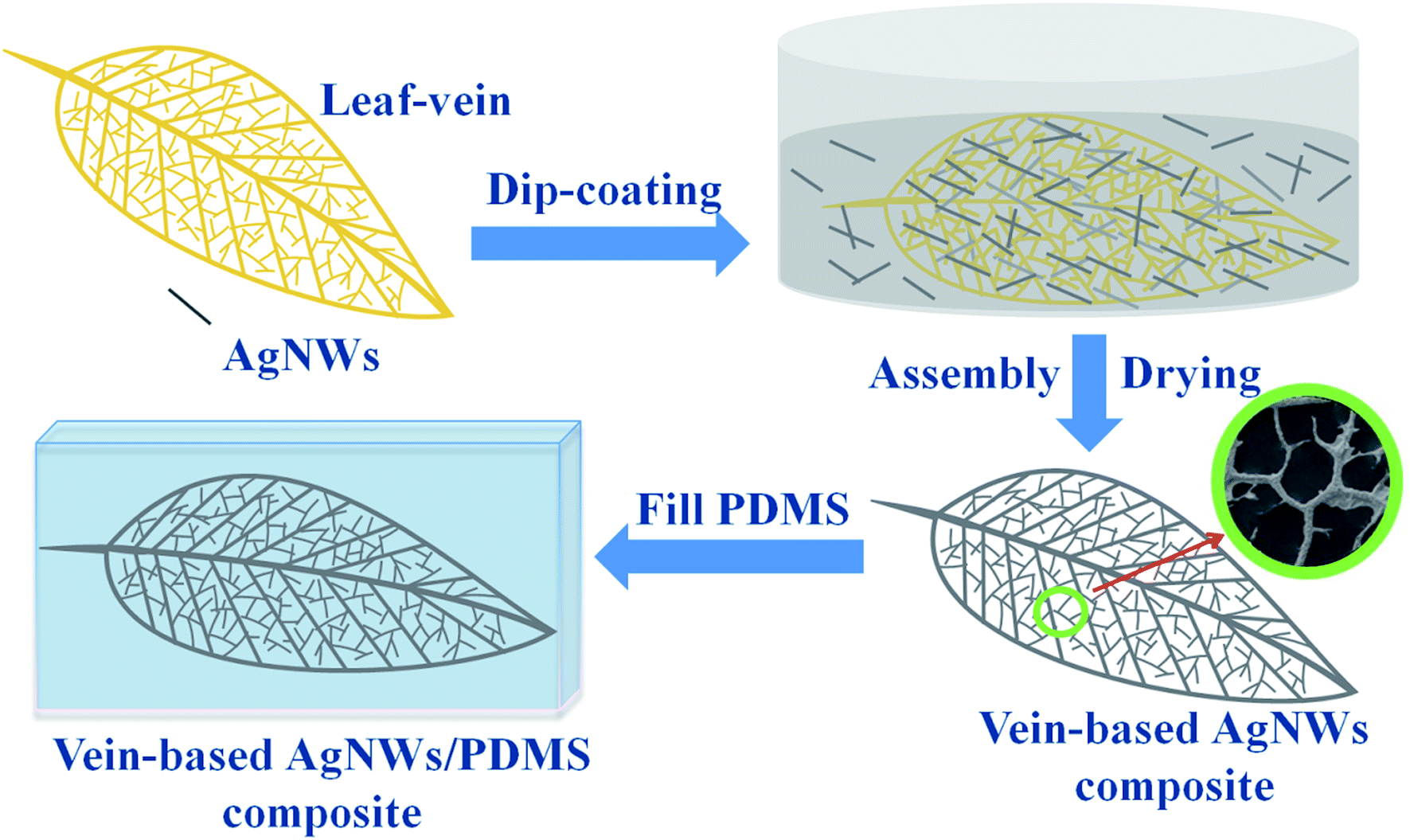 | ||
| Fig. 1 A schematic of the fabrication process for the vein–AgNWs–PDMS stretchable composite. | ||
According to previous reports, the content of conductive material in conductors has great influence on the conductivity of conductor.7,9 Herein, the AgNWs were expected to have the same effect, with the resistance of the vein–AgNWs–PDMS composite controlled through adjusting the number of cycles of dip-coating. As shown in Fig. 2a, the vein network was a quasi-fractal network structure and the surface of the pristine vein was smooth, while AgNWs adhered tightly to the surface of the vein were clearly observed after the dip-coating process. The binary-network of the vein–AgNWs composites was constructed by interconnected vein fibers and the AgNWs network, which is shown in SEM images. This fabrication process was different to the single conductive network in previous vein-based conductors20,21 and some AgNWs-based conductors.4,7,8,15 As revealed in Fig. 2b–d, the density of AgNWs on the vein surface increased with the number of cycles of the dipping process, which was also reflected in the increase of AgNW content in the samples. As shown in Fig. 3a, the weight loss of pure vein was about 96% when heating up to 800 °C, so it can be considered that the remaining weight of the other three samples was the sum of silver and the 4% mass of vein in the sample. The mass fraction of AgNWs in the vein–AgNWs composites can be calculated and was found to be 10%, 21% and 37% as the number of dipping cycles increased from one to three. Moreover, these samples exhibited varied electrical properties in the following tests.
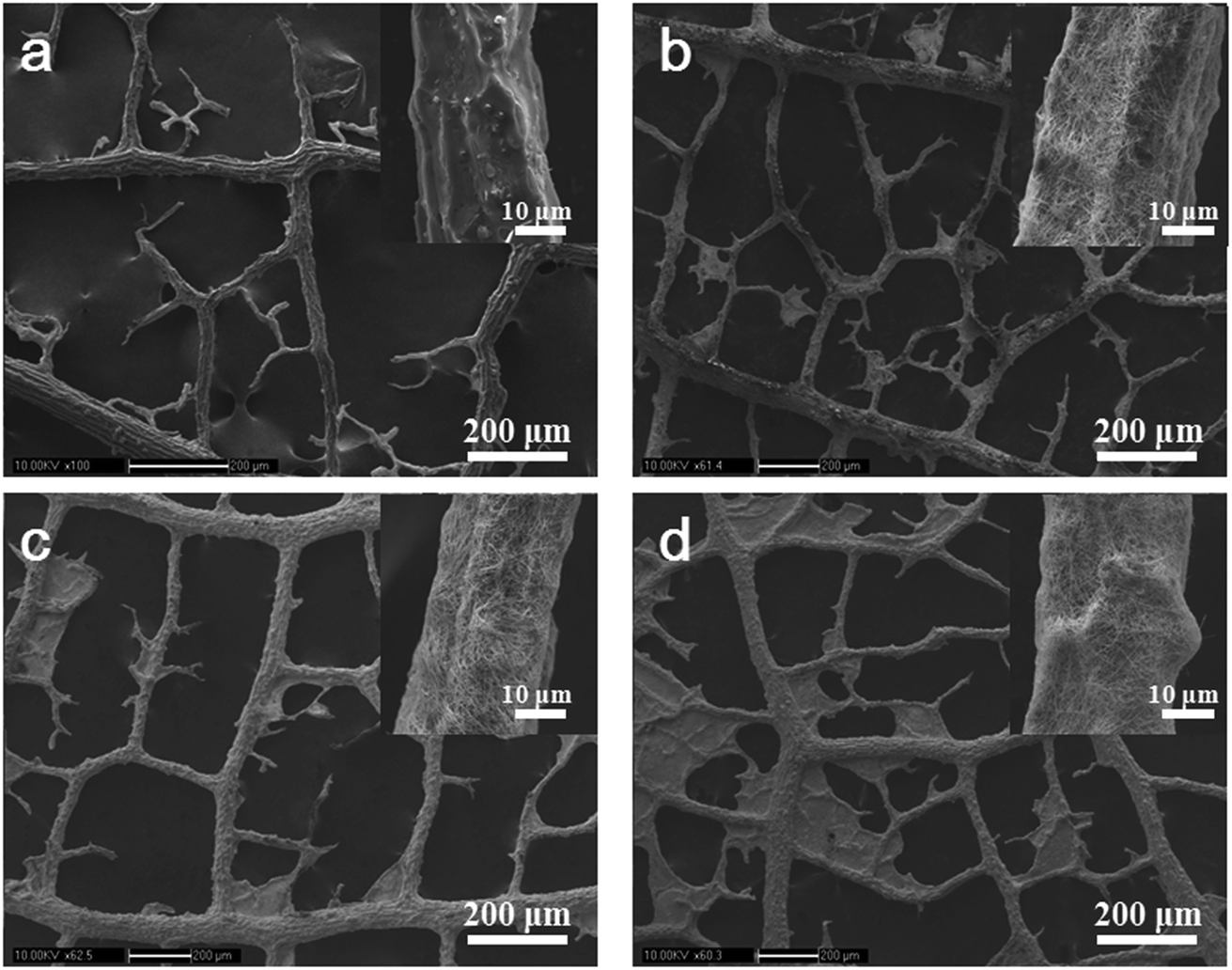 | ||
| Fig. 2 Surface morphology of (a) pristine vein and (b–d) vein–AgNWs composites with different numbers of cycles of dipping: (b) one, (c) two and (d) three. | ||
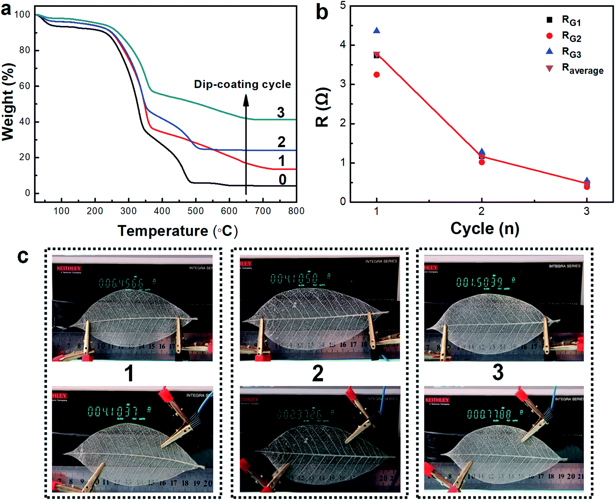 | ||
| Fig. 3 (a) Thermogravimetric analysis of pristine vein and vein–AgNWs composites prepared with different numbers of dipping cycles. (b) Resistance values and average resistance of three groups of samples prepared with different numbers of dipping cycles. (The veins selected in each group are similar as much as possible and the distance between the two clamps on the sample surface was 8 cm.) (c) Pictures showing the resistance of the vein–AgNWs composites prepared with different numbers of dipping cycles. | ||
The resistance of the vein–AgNWs composite changed with the number of dip-coating cycles confirming the controllability of conductivity. As shown in Fig. 3b, three groups of repeated experiments have been done to explore the influence of the number of dipping cycles on the resistance of the samples, where similar veins were selected as much as possible in each group of experiment. The resistance of the samples with the same number of dipping cycles was different due to differences in the density of veins, but the overall results show that the resistance decreases with increasing number of dipping cycles. Moreover, the resistance of the vein–AgNWs composite decreased as the measurement distance of the composites decreased. As shown in Fig. 3c, the resistance changed from 6.4 Ω to 1.5 Ω as the number of dipping cycles increased from one to three with a measurement distance of about 10 cm. When the measurement distance was reduced to about 6 cm, the resistances of these composites were 4.1 Ω, 2.3 Ω and 0.77 Ω, respectively. The results were better than those for the vein-based conductor in previous reports, where the resistance was just 4.1 Ω with a shorter measurement distance.21
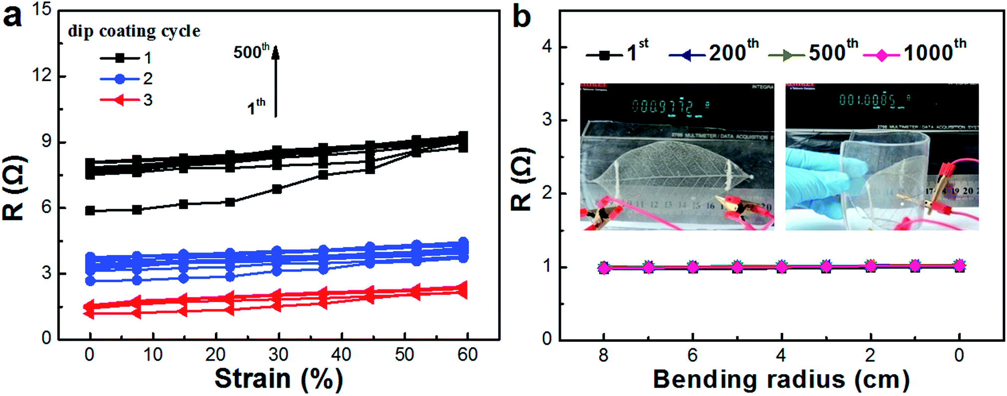
The electrical and mechanical properties are key points for stretchable conductors. In this work the conductivity of the samples increases from 43.1 S cm−1 to 257.7 S cm−1 when the number of dipping cycles increases from one to three. The results indicated that the conductivity of the electrodes can be tuned easily by adjusting the number of dipping cycles. The electrical conductivity of the vein–AgNWs–PDMS composite is much better than that of some other previously reported conductors, such as the AgNWs 2D mass-spring networks prepared by floating compression or using a spray-roll coating process to fabricate metal wire network-based transparent electrodes. Furthermore, these preparation methods are more complicated than the procedure presented here.26,29 In addition, the electromechanical stability of STCs plays an important role in practical applications. Thus the electrical properties of the vein–AgNWs–PDMS conductor under tensile stress were studied. As shown in Fig. 4a, resistance variations of three samples were studied while the tensile strain increased from 0% to 60%. It can be clearly observed that the vein–AgNWs–PDMS conductor with a higher number of dipping cycles has better electromechanical stability during the stretching process, which demonstrates that the electromechanical stability of the vein–AgNWs–PDMS composite can be enhanced by adjusting the content of AgNWs. Fig. 4b shows that the vein–AgNWs–PDMS composite prepared by dipping the vein into the AgNW dispersion three times can remain conductive under a tensile strain of 150%, and the resistance changed from 0.97 Ω to 5.47 Ω (Fig. 5), which is better than the previous reported vein-based copper conductor which lost conductivity under a tensile strain of 70%.21 An LED illuminated by using this sample as the connecting wire at different strains (0%, 30%, 50%, 70%, 100% and 150%) is shown in Fig. S1.† The brightness of the LED lights has a slight change during the whole stretching process, which indicated that the conductivity of the vein–AgNWs–PDMS conductor can be mostly retained under large tensile stress. Moreover, the introduced PDMS matrix can make the AgNW network more mechanically robust,24 which was demonstrated through the control experiment (Fig. S2†). The excellent electromechanical stability of the vein–AgNWs–PDMS conductor is not only related to the content of AgNWs in the conductor, but more importantly the binary structure network of the vein–AgNWs–PDMS composite.
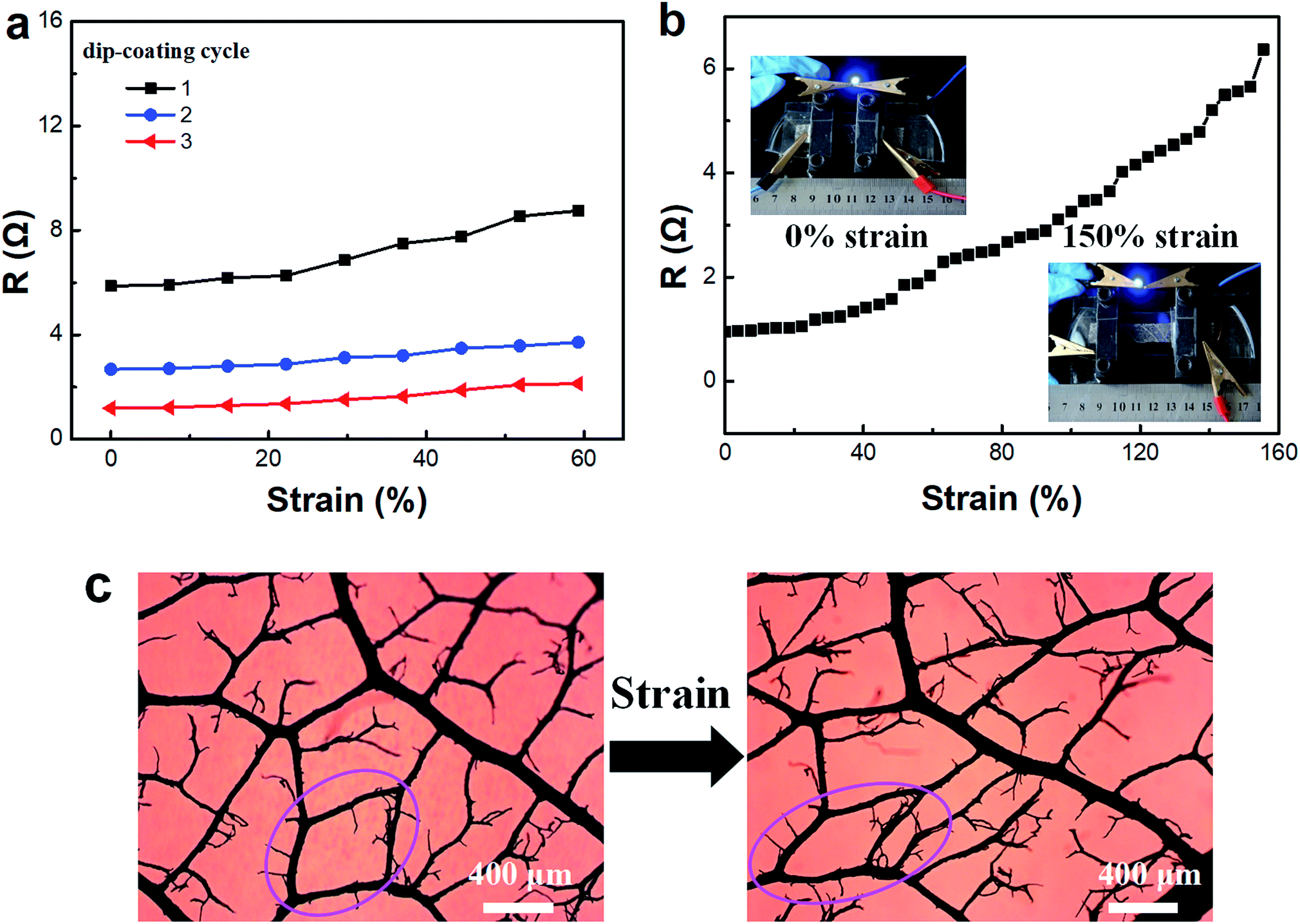 | ||
| Fig. 4 (a) Resistance as a function of strain (from 0 to 60%) of the vein–AgNWs–PDMS composites prepared using different numbers of dipping cycles. (The space between the two copper electrodes of the samples is 4 cm.) (b) Resistance as a function of strain (from 0% to 155%) of the vein–AgNWs–PDMS composite prepared by dipping three times during the first stretching test. Inset: photographs of an LED circuit installation using the vein–AgNWs–PDMS composites as interconnects under 0% and 150% strain. (c) Optical microscope images of the change in shape of the vein network under tensile strain. (The spot size of transmission light on the sample is about 2 × 2.7 mm.) | ||
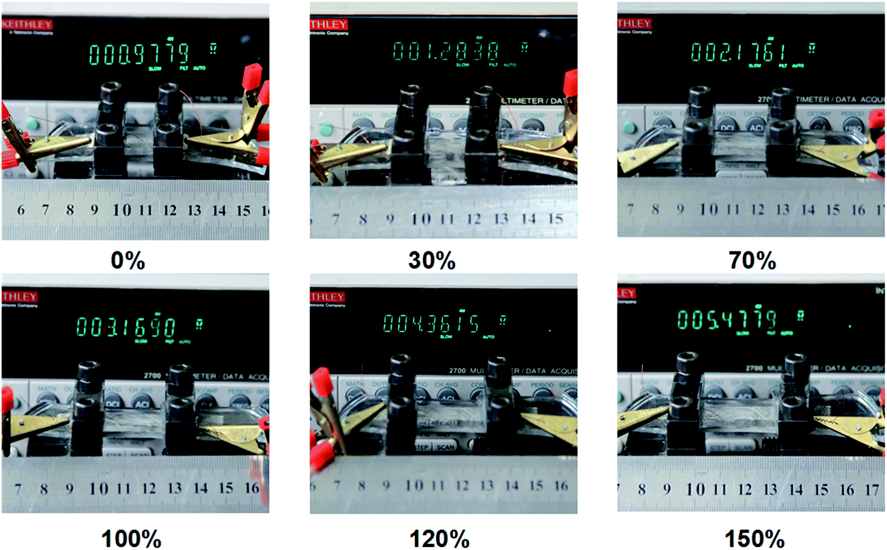 | ||
| Fig. 5 Digital photos of the resistance of the vein–AgNWs–PDMS composite (three dipping cycles) at 0%, 30%, 70%, 100%, 120% and 150% strain during the 1st stretching test. | ||
To further understand the relation between the binary structure network and its performance, the structure deformation under stress was observed using an optical microscope. As shown in Fig. 4c, the macropores of the vein network (marked by the purple window) elongated in the direction of the applied force and shrank in the perpendicular direction when a tensile stress was applied to the vein–AgNWs composites. Meanwhile, the interconnected 2D AgNW network can also effectively release stress through deformation to avoid damaging the conductive path under tensile strain. In short, the deformation of the stretchable binary structure under stress led to excellent electromechanical properties.
The effects of tensile cycles on the resistance of the vein–AgNWs–PDMS composite were also studied. Vein–AgNWs–PDMS conductors prepared by dipping a different number of times (one, two and three) were stretched from 0% to 60% strain for 500 cycles. Fig. 6a shows that the resistance of the vein–AgNWs–PDMS composite increased as the number of stretching cycles increased firstly, and then remained stable during the following stretching process. Compared with the vein–AgNWs–PDMS composites prepared with lower numbers of dip-coating cycles, the variation in the resistance of the higher one was much smaller. This reaffirmed that the higher the mass fraction of AgNWs in the conductor, the better the electromechanical stability. These results were also consistent with the conclusion mentioned above, that the properties of the vein–AgNWs–PDMS composites can be easily improved through tuning the number of dip-coating cycles. Apart from the initial increase in resistance in the first several stretching cycles, the resistance remained constant, indicated that these vein–AgNWs–PDMS composites could be used as potential interconnects in related electronic devices. This conclusion was later demonstrated via observing the structural changes of the veins in the stretching–relaxing process using an optical microscope. As shown in Fig. S3,† the vein structure was elongated along the stress direction and restored after releasing the stress. The influence of the dual network structure on the stability of the mechanical and electrical properties was further illustrated. Meanwhile, PDMS has a protective effect on the structure and enhances structure recovery.
 | ||
| Fig. 6 (a) Resistance curves of the vein–AgNWs–PDMS composites prepared with different numbers of dipping cycles under stretching from 0% to 60% strain for 500 cycles. (b) Resistance curve of the vein–AgNWs–PDMS conductor prepared with three dipping cycles under bending from a radius of 8 cm to 0 cm for 1000 cycles. (The photographic images show the resistance of the sample under a bending radius of 8 cm and folding after 1000 cycles of bending.) | ||
In addition, the effects of bending on the conductive properties of the vein–AgNWs–PDMS composites were studied. The samples used for the bending test were prepared from the whole leaf vein. As shown in Fig. 6b, the vein–AgNWs–PDMS composite prepared by dipping the vein into AgNW dispersion three times was bent to various radii of curvature until it was almost folded. The resistance curve as a function of the radius of curvature from the 1st to the 1000th cycle is very flat. It can be clearly observed that the resistances were 0.97 Ω and 1.00 Ω at radii of curvature of 8 cm and 0 cm, respectively, during the 1000th bending cycle. These results show that the vein–AgNWs–PDMS composites can maintain good conductivity under certain stretching and bending. In other words, the vein–AgNWs–PDMS composites have excellent electromechanical properties and potential for application in high performance deformable devices.
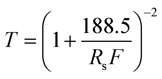
The transmittances of the vein–AgNWs–PDMS composites were also investigated. Herein, the samples selected for transparency testing have a relative uniform network density and the size of the samples was controlled at about 1 cm × 5 cm. Therefore, the measured transparency of the sample could be estimated as the value of the whole sample. As shown in Fig. 7a, the transmittance of the samples decreased as the number of dipping cycles increased. The sheet resistance (RS) and transmittance (T) of the composites mainly correspond to the density of AgNWs on the vein surface. As shown in the SEM images in Fig. 2, the thickness on the vein fiber covered by AgNWs increased with increasing number of cycles of dipping, which led to a slight reduction in the transmittance of the vein–AgNWs–PDMS conductor. Even so, the red flower below the vein–AgNWs–PDMS conductors prepared with various numbers of dipping cycles can be observed clearly in Fig. 7c–e. At a wavelength of 550 nm, the transmittance of the samples decreased from 74% to 56% when the number of dipping cycles increased from one to three while the sheet resistance decreased from 1 to 0.22 Ω sq−1. The relation between T and RS of the composites can be quantitatively analyzed through20,23,30,31,34
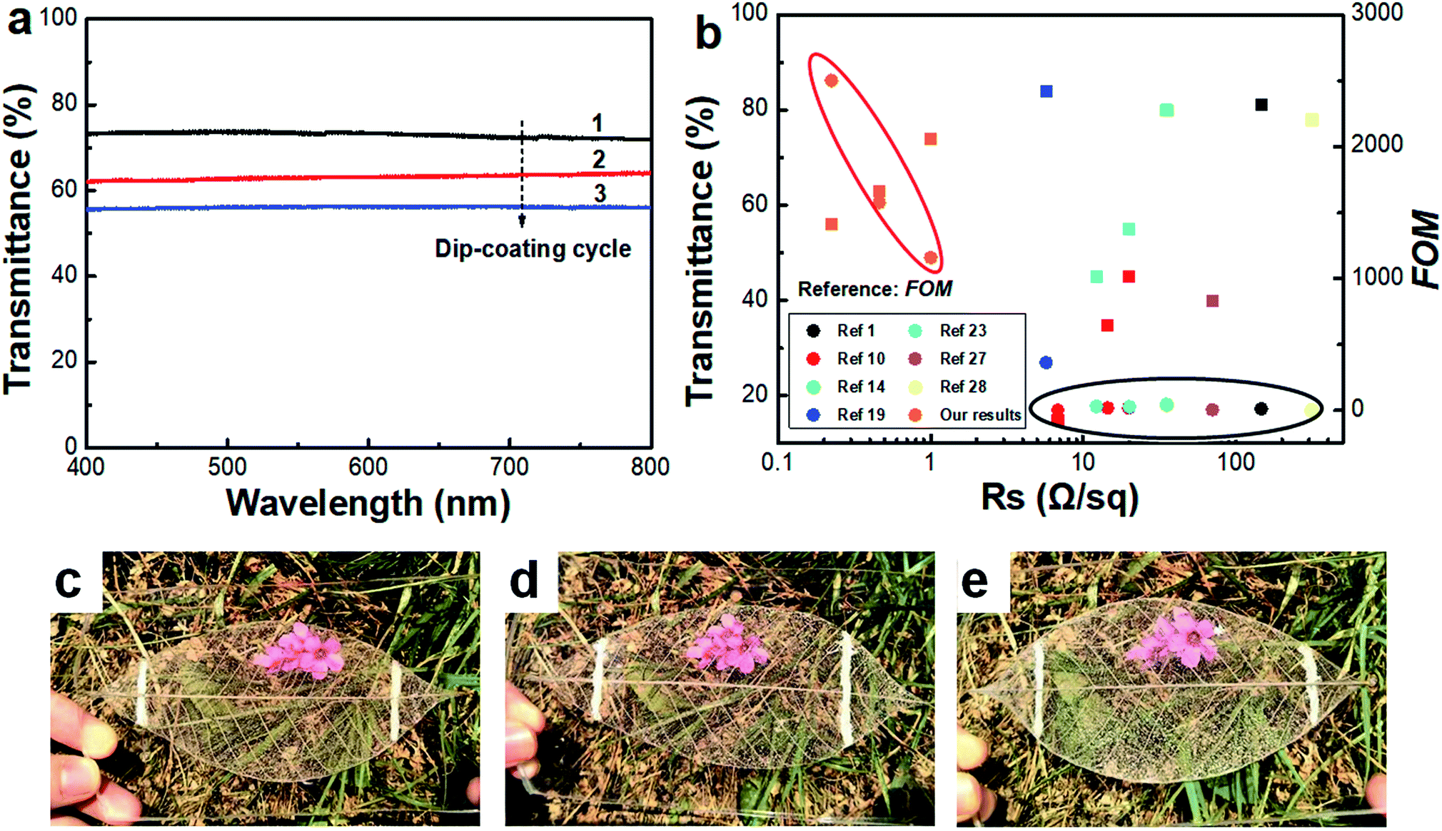 | ||
| Fig. 7 (a) Optical transmittance of the vein–AgNWs–PDMS composites prepared by different numbers of cycles of dipping (one, two and three). (b) Comparison of the vein–AgNWs–PDMS composites with other transparent conductors reported in the literature in terms of the average sheet resistance on a log scale and FoM with related transmittance at 550 nm. (The squares and circles represent the values of transmittance and FoM, respectively, and the same color represents the same composite.) (c–e) Photographs of the vein–AgNWs–PDMS composites over a pink flower. The samples were prepared by different numbers of dipping cycles: (c) one, (d) two and (e) three. | ||
However, the transmittance of the vein–AgNWs–PDMS composites was not ideal compared to some AgNW based transparent conductors reported recently.26,31–34 However, these transparent conductors have a great limitation in the electrical mechanical properties, which also limits the use of such highly transparent conductors in stretchable devices. In this work, the transmittance of the vein–AgNWs–PDMS composites mainly depended on the density and material of the veins, which can be further improved by choosing an appropriate vein.20,21 Although the interconnected vein structure endows high conductivity during the stretching process, a slight shadow was shown in the transmission of light.
Due to the excellent electromechanical properties of the vein–AgNWs–PDMS composite, the composites can be directly used for high performance flexible electronic devices. Besides the conductor wire used as mentioned above, herein, we fabricated flexible LED arrays (Fig. 8) using the vein–AgNWs–PDMS composites as the semi-transparent interconnects. Different patterns of LED array (Fig. 8b and d) were fabricated according to demands, and furthermore, it can be seen clearly that the LED arrays maintained a stable brightness under deformation as shown in Fig. 8b–d. However, such LED arrays cannot work well under tensile force because the connection between the bulb and the conductor would be destroyed by tensile stress.
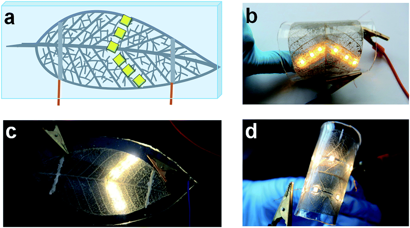 | ||
| Fig. 8 LED arrays using the vein–AgNWs–PDMS composites prepared with three dipping cycles as interconnects. (a) A schematic of the 2D LED array, (c) optical images of the 2D LED array and (b and d) different 2D LED arrays under bending. | ||
In addition to the excellent electromechanical properties mentioned above, the vein–AgNWs–PDMS composite can also efficiently absorb NIR light to generate heat for local heating due to the existence of the AgNWs.36,37 The photo-thermal property of AgNWs was usually used in optical post-processing methods for AgNW networks,38 but this method has not been used in the local heating of the transparent conductor. Herein, the local heating of the vein–AgNWs–PDMS composite is realized by laser irradiation based on the photo-thermal effect of the AgNWs.
To investigate the photo-thermal properties of the vein–AgNWs–PDMS composite, as shown in Fig. 9a, a position heating experiment was designed. A local area of the composite surface was irradiated by a NIR laser, in which heat generated immediately. As shown in Fig. 9b, the temperature of the local area increased with an increase in the power and irradiation time, which indicated that the energy of the NIR laser can be instantly turned into heat by the vein–AgNWs–PDMS composite. For example, the temperature of the surface of the sample increased from 26.2 °C to 83.4 °C after being irradiated for 60 seconds under laser light with a power of 2 W. The elevated temperature was lower than the curing temperature of PDMS and had little impact on the resistance due to the dense AgNW network on the vein.38 Therefore, it has no significant effect on the electrical and mechanical properties of the conductors. The vein with a macroporous structure is beneficial for releasing heat and avoiding local overheating. As revealed in Fig. 9c, the thermal distribution of the local area under laser irradiation was obtained by an infrared thermometer. The color changed from white to black, which indicated that heat was delivered from the laser point to the surroundings. In addition, a comparative experiment was carried out to explore the influence of PDMS on the photo-thermal performance of the conductor. The temperature of the vein–PDMS composite with no AgNWs was almost unchanged under irradiation (Fig. S4†), and this result also verified that the photo-thermal performance of the conductor depended mainly on the AgNWs.
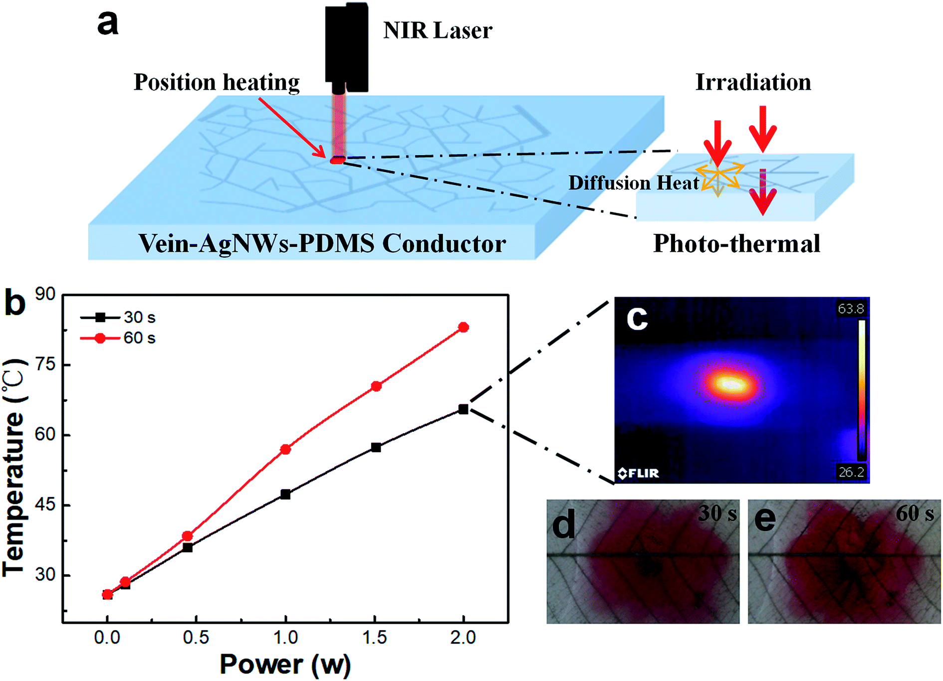 | ||
| Fig. 9 (a) Schematic illustration of position heating with the vein–AgNWs–PDMS conductor as a semi-transparent heater. (b) Power-dependent temperature variations of the vein–AgNWs–PDMS composite under 808 nm NIR light irradiation at a distance of 10 cm for 30 seconds and 60 seconds. (c) Infrared camera thermal image of a vein–AgNWs–PDMS composite irradiated for 30 seconds under laser light with power of 2 W. (d and e) A demisting test: the sample (frozen in a refrigerator for 3 h) surface was irradiated by laser light with a power of 2 W at room temperature for different times, (d) 30 seconds and (e) 60 seconds. (The 808 nm NIR laser irradiation had a spot size of 1 × 0.5 cm2 and all test samples were prepared using two dipping cycles.) | ||
In order to study the effectiveness of the heating provided by the photothermal properties of the vein–AgNWs–PDMS composite a demisting test was performed. The sample was frozen at −20 °C for 3 h and then exposed to room temperature air. A film of moisture rapidly condenses on the sample surface forming a light diffusing layer. A fixed area of the sample surface was irradiated by an IR laser at room temperature. This resulted in local heating of the vein–AgNWs–PDMS composite removing the moisture layer in a particular region. This can be seen in Fig. 9d and for contrast a red flower was placed under the sample to highlight the removal of the condensates. The flower can be clearly seen in the central region of the image as this has been locally heated but remains hazy beyond this region due to the continued presence of the condensate. As shown in Fig. 9e, the demisted region continues to expand as the heating time is increased to 60 s. The reason for this is that the heat was generated on a fixed area through the absorption of laser light by the AgNWs, which made the icy fogs melt on a specific area of the surface of the vein–AgNWs–PDMS composite. The clear area then gradually expanded with the increase in irradiation time, which also demonstrated that the heat can be effectively diffused to avoid overheating. For a transparent heater, Coleman and Bellet have developed a comprehensive model, which can be used as a figure of merit to assess the performance.39 However, this model only applies to transparent heater films which can be heated by voltage application. Compared to transparent heaters based on the electrothermal effect which can only achieve the overall heating by switching on the electric power, the vein–AgNWs–PDMS composites can realize position heating without electric power, developing a new application of the vein–AgNWs–PDMS composite as a heater for specific position heating.7,20,40
3. Conclusion
In summary, hierarchical vein-based AgNWs composites were embedded in PDMS to fabricate stretchable semi-transparent vein–AgNWs–PDMS composites with excellent electrical conductivity. A vein–AgNWs–PDMS composite with a transmittance of 74% at 550 nm and sheet resistance of 1 Ω sq−1 was obtained. The electrical conductivity of the vein–AgNWs–PDMS composites can reach 257.7 S cm−1 when the number of dipping cycles is up to three, which can be adjusted easily by tuning the number of cycles of the dipping process. The binary-network conductive structure of the vein–AgNWs–PDMS composite is essential to its excellent electromechanical stability, which allowed the vein–AgNWs–PDMS composite to have a high conductance at 150% tensile strain. Furthermore, the excellent electrical conductivity of the vein–AgNWs–PDMS composites remains almost constant during the fatigue tests of bending (1000 cycles, radius from 8 cm to 0) and stretching (500 cycles, stretched from 0% to 60%). The vein–AgNWs–PDMS composites have been demonstrated as high-performance patterned electrodes and flexible interconnects that are appropriate to be used in stretchable electronic devices. In addition, the vein–AgNWs–PDMS composites can be used as a heater for position heating due to the excellent photo-thermal properties and good heat dissipation effect. The facile preparation method and the cheap and abundant raw materials make the nature-inspired stretchable semi-transparent conductive composites promising materials for related electronic equipment or heating films with special conditions in future.4. Experimental section
4.1 Materials
Silver nitrate (AgNO3), polyvinylpyrrolidone (PVP, K30) and sodium chloride were supplied by Sinopharm. Polydimethylsiloxane (PDMS, Sylgard 184) was purchased from Dow Corning. Silver paste was obtained from SPI. Leaf veins of oak with lengths of 10–15 cm were purchased from an online store.4.2 Preparation of vein–AgNWs–PDMS
The intact leaf vein was cleaned using ethanol or deionized water several times and air dried at room temperature for use. The AgNWs were synthesized through chemical reduction of Ag ions as reported previously with a slight difference.24,25 The gentle stirring was changed from 50 rpm to 30 rpm resulting in longer AgNWs. The AgNWs obtained were washed with isopropanol three times and dispersed in isopropanol. Then veins were soaked into the isopropanol solution of AgNWs. After that, samples were picked out and dried at room temperature. Different samples were prepared by changing the number of dipping cycles (one, two and three, dipping again after the solvent on the vein was evaporated totally). Finally, copper wires were connected to both ends of the as-prepared samples through silver paste. The distance between the two copper wires on the sample surface was 8 cm for the bending test and 4 cm for the stretching test. The size of the sample for the stretching test was 5.5 × 1 cm2. The samples were then transferred into petri dishes after the silver paste was fully fixed. The as-prepared samples were fully covered by a mixture of PDMS precursor (mixing the “base” and the “curing agent” with a ratio of 10![[thin space (1/6-em)]](https://www.rsc.org/images/entities/char_2009.gif) :1, w/w, Sylgard 184), followed by deflating in a vacuum baking oven for 30 min and curing for 2 h in a dry oven at 90 °C. The vein–AgNWs–PDMS composites were then obtained by peeling off the composites from the petri dish.
:1, w/w, Sylgard 184), followed by deflating in a vacuum baking oven for 30 min and curing for 2 h in a dry oven at 90 °C. The vein–AgNWs–PDMS composites were then obtained by peeling off the composites from the petri dish.
4.3 Preparation of LED arrays
An LED circuit and 2D LED arrays using the vein–AgNWs–PDMS conductor with different shapes as semi-transparent interconnects were prepared for the flexible electronic device experiment. Herein, the LEDs were fixed to the vein–AgNWs composite using silver paste, and then fully covered by a mixture of PDMS precursor. The LED arrays were obtained after the curing of the PDMS.4.4 Photo-thermal properties of vein–AgNWs–PDMS
Vein–AgNWs–PDMS samples were subject to 808 nm NIR laser irradiation with a spot size of 1 × 0.5 cm2 with different powers at a distance of 10 cm. The temperature of the local surface which was irradiated by laser light was measured with an infrared thermometer immediately upon removal of the laser. This further investigated the ability of the vein–AgNWs–PDMS composite as a transparent heater for position heating. A vein–AgNWs–PDMS conductor was placed in the refrigerator and frozen for 3 h and then the local surface of the vein–AgNWs–PDMS conductor was exposed to a laser (the distance between laser and surface was 5 cm) with a power of 2 W at room temperature.4.5 Characterization
Stretching tests were conducted using home-made equipment. The electrical resistance of the vein–AgNWs–PDMS composite was measured using a custom built automated 4-point probe measurement system connected to a Keithley 2700 multi-source meter.Scanning electron microscopy (SEM) and optical microscopy were used to characterize the surface morphology of the samples. The thickness of a vein was about 0.16 mm measured by a slide caliper rule. The transmittance spectra were measured using a UV-vis spectrometer (TU-1901). The surface morphology of vein and vein–AgNWs composites was observed by SEM (CamScan Apollo 300). The mass loading of AgNWs was calculated from the residual mass determined by thermogravimetric analysis on a Mettler TGA1 instrument (50 °C to 800 °C) at a heating rate of 10 °C min−1 in a nitrogen atmosphere.
Conflicts of interest
There are no conflicts to declare.Acknowledgements
This work is financially supported by the National Natural Science Foundation of China (Grants: 21407134, 21404094, 11572295 and 11372290).References
- A. Shimoni, S. Azoubel and S. Magdassi, Nanoscale, 2014, 6, 11084 RSC.
- T. Q. Trung and N. E. Lee, Adv. Mater., 2017, 29, 1603167 CrossRef PubMed.
- J. Wang, M. Liang, Y. Fang, T. Qiu, J. Zhang and L. Zhi, Adv. Mater., 2012, 24, 2874 CrossRef PubMed.
- J. Krantz, T. Stubhan, M. Richter, S. Spallek, I. Litzov, G. J. Matt, E. Spiecker and C. J. Brabec, Adv. Funct. Mater., 2013, 23, 1711 CrossRef.
- T. Q. Trung and N. E. Lee, J. Mater. Chem. C, 2017, 5, 2202 RSC.
- S. Hiesang, Y. S. Woo, W. Shinb, D.-J. Yun, T. Lee, F. S. Kimd and J. Hwange, Appl. Surf. Sci., 2017, 419, 63 CrossRef.
- X. He, R. He, A. Liu, X. Chen, Z. Zhao, S. Feng, N. Chen and M. Zhang, J. Mater. Chem. C, 2014, 2, 9737 RSC.
- D. S. Leem, A. Edwards, M. Faist, J. Nelson, D. D. C. Bradley and J. C. D. Mello, Adv. Mater., 2011, 23, 4371 CrossRef PubMed.
- S. Narayanan, J. Choi, L. Porter and M. R. Bockstaller, ACS Appl. Mater. Interfaces, 2013, 5, 4093 CrossRef PubMed.
- L. Cai, J. Li, P. Luan, H. Dong, D. Zhao, Q. Zhang, X. Zhang, M. Tu, Q. Zeng, W. Zhou and S. Xie, Adv. Funct. Mater., 2012, 22, 5238 CrossRef.
- E. T. Alonso, G. Karkera, G. F. Jones, M. F. Craciun and S. Russo, ACS Appl. Mater. Interfaces, 2016, 8, 16541 CrossRef PubMed.
- B. W. An, B. G. Hyun, S. Y. Kim, M. Kim, M. S. Lee, K. Lee, J. B. Koo, H. Y. Chu, B. S. Bae and J. U. Park, Nano Lett., 2014, 14, 6322 CrossRef PubMed.
- H. L. Ferrand, S. Bolisetty, A. F. DemirÖrs, R. Libanori, A. R. Studart and R. Mezzenga, Nat. Commun., 2016, 7, 12078 CrossRef PubMed.
- T. Akter and W. S. Kim, ACS Appl. Mater. Interfaces, 2012, 4, 1855 CrossRef PubMed.
- Y. Jia, C. Chen, D. Jia, S. Li, S. Ji and C. Ye, ACS Appl. Mater. Interfaces, 2016, 8, 9865 CrossRef PubMed.
- L. Dou, F. Cui, Y. Yu, G. Khanarian, S. W. Eaton, Q. Yang, J. Resasco, C. Schildknecht, K. Schierle-Arndt and P. Yang, ACS Nano, 2016, 10, 2600 CrossRef PubMed.
- J. Groep, P. Spinelli and A. Polman, Nano Lett., 2012, 12, 3138 CrossRef PubMed.
- D. S. Ghosh, T. L. Chen, V. Mkhitaryan and V. Pruneri, ACS Appl. Mater. Interfaces, 2014, 6, 20943 CrossRef PubMed.
- T. Tokuno, M. Nogi, J. Jiu, T. Sugahara and K. Suganuma, Langmuir, 2012, 28, 9298 CrossRef PubMed.
- B. Han, Y. Huang, R. Li, Q. Peng, J. Luo, K. Pei, A. Herczynski, K. Kempa, Z. Ren and J. Gao, Nat. Commun., 2014, 5, 5674 CrossRef PubMed.
- Y. Yu, Y. Zhang, K. Li, C. Yan and Z. Zheng, Small, 2015, 11, 3444 CrossRef PubMed.
- S. Ye, A. R. Rathmell, Z. Chen, I. E. Stewart and B. J. Wiley, Adv. Mater., 2014, 26, 6670 CrossRef PubMed.
- Y. Ko, S. K. Song, N. H. Kim and S. T. Chang, Langmuir, 2016, 32, 366 CrossRef PubMed.
- J. Ge, H.-B. Yao, X. Wang, Y.-D. Ye, J.-L. Wang, Z.-Y. Wu, J.-W. Liu, F.-J. Fan, H.-L. Gao, C.-L. Zhang and S.-H. Yu, Angew. Chem., Int. Ed., 2013, 52, 1654 CrossRef PubMed.
- C. Zhu, L. Li, J. Wang, Y. Wu and Y. Liu, RSC Adv., 2017, 7, 51 RSC.
- B. S. Kim, J. B. Pyo, J. G. Son, G. Zi, S. S. Lee, J. H. Park and J. Lee, ACS Appl. Mater. Interfaces, 2017, 9, 10865 CrossRef PubMed.
- F. Xu, X. Wang, Y. Zhu and Y. Zhu, Adv. Funct. Mater., 2012, 22, 1279 CrossRef.
- J. Wan, F. Gu, W. Bao, J. Dai, F. Shen, W. Luo, X. Han, D. Urban and L. Hu, Nano Lett., 2015, 15, 3763 CrossRef PubMed.
- S. Kiruthika, R. Gupta, A. Anand, A. Kumar and G. U. Kulkarni, ACS Appl. Mater. Interfaces, 2015, 7, 27215 CrossRef PubMed.
- T. Gao, Z. Li, P. Huang, G. J. Shenoy, D. Parobek, S. Tan, J. Lee, H. Liu and P. W. Leu, ACS Nano, 2015, 9, 5440 CrossRef PubMed.
- X. Zhang, J. Wu, J. Wang, Q. Yang, B. Zhang and Z. Xie, ACS Appl. Mater. Interfaces, 2016, 8, 34630 CrossRef PubMed.
- Y. Kim, S. Jun, B. K. Ju and J. W. Kim, ACS Appl. Mater. Interfaces, 2017, 9, 7505 CrossRef PubMed.
- Y. Jin, K. Wang, Y. Cheng, Q. Pei, Y. Xu and F. Xiao, ACS Appl. Mater. Interfaces, 2017, 9, 4733 CrossRef PubMed.
- G. S. Liu, J. S. Qiu, D. H. Xu, X. Zhou, D. Zhong, H. P. D. Shieh and B. R. Yang, ACS Appl. Mater. Interfaces, 2017, 9, 15130 CrossRef PubMed.
- T. Sannicolo, M. Lagrange, A. Cabos, C. Celle, J.-P. Simonato and D. Bellet, Small, 2016, 12, 6052 CrossRef PubMed.
- M. Wu, Y. Li, N. An and J. Sun, Adv. Funct. Mater., 2016, 26, 6777 CrossRef.
- Y. Li, S. Chen, M. Wu and J. Sun, ACS Appl. Mater. Interfaces, 2014, 6, 16409 CrossRef PubMed.
- J. A. Spechler, K. A. Nagamatsu, J. C. Sturm and C. B. Arnold, ACS Appl. Mater. Interfaces, 2015, 7, 10556 CrossRef PubMed.
- S. Sorel, D. Bellet and J. N. Coleman, ACS Nano, 2014, 8, 4805 CrossRef PubMed.
- C. Hudaya, B. Jeon and J. Lee, ACS Appl. Mater. Interfaces, 2015, 7, 57 CrossRef PubMed.
Footnote |
| † Electronic supplementary information (ESI) available. See DOI: 10.1039/c8ra02064g |
| This journal is © The Royal Society of Chemistry 2018 |