
 Open Access Article
 This Open Access Article is licensed under a Creative Commons Attribution-Non Commercial 3.0 Unported Licence
Polarization-independent enhancement of graphene plasmons by coupling with the dipole-like near field of the metallic split-mesh structure
Anqi Yu *ab
*ab
aState Key Laboratory of Infrared Physics, Shanghai Institute of Technical Physics, Chinese Academy of Sciences, 500 Yutian Road, Shanghai, 200083, China. E-mail: yuanqi@mail.sitp.ac.cn
bUniversity of Chinese Academy of Sciences, No. 19 A Yuquan Road, Beijing, 100049, China
First published on 19th June 2018
Abstract
The localized electric field enhancement of graphene plasmon modes is limited by the duty cycle of graphene, the frequency, the absorption and the scattering rate. To obtain higher detectivity, higher field enhancement is required. While the absorption can be no larger than 100%, the scattering is an intrinsic limitation, and the frequency is designated, the duty cycle is the only parameter that can be designed freely to achieve high field enhancement. By etching graphene into periodic structures, i.e. reducing the duty cycle of graphene, the localized electric field can be enhanced as a result of the reduction of the active region. However, too small a duty cycle will weaken the coupling efficiency, which will reduce the absorption, and then the localized electric field can hardly be further enhanced. In this work, we propose to use the metallic split-mesh structure which will focus the incident radiation at the ends of the metallic bars. The absorption and the electric field will be greatly enhanced by placing graphene structures below the small holes formed by the metallic split-mesh structure.
Introduction
Terahertz (THz) waves have attracted a great deal of interest in recent years. THz waves offer an alternative approach for imaging through many materials which are opaque to other electromagnetic waves. They can also be utilized to detect many bio-macromolecules because these molecules have rotation or vibration energies in the terahertz frequencies. For cosmology, a large portion of space radiation is within the terahertz range, so THz technologies are helpful for developing cosmology. However, the commercially available terahertz devices have many weaknesses such as the requirement of working in cryogenic temperatures, bulky size or the lack of tunability. Fortunately, surface plasmons offer an approach to solve these problems.Surface plasmons are the collective oscillation of charge carriers at the interface of the two-dimensional electron gas and the dielectric. The abilities of manipulating the incident light and confining incident radiation at the vicinity of the interface offer surface plasmons the potential for use in waveguides,1–3 modulators,4–7 polarization converters,8–10 absorbers,11–13 etc. Plasmon-based devices are especially attractive at the THz frequencies because they can tightly confine the incident light at the dielectric/semiconductor or dielectric/conductor interface, which can help to solve the aforementioned problems of current commercial terahertz devices.
For many potential applications of the terahertz technology, such as wireless communication or the detection of cosmic radiations, the received signal can be quite weak. For the identification of macromolecules, the concentration of the target molecules can be very low, so that the scattering or the reflection can also be weak. Therefore, detectors with high detectivity are required. As the detectivity is decided by the responsivity and the density of dark current, enhancing the absorption of the devices, which results in high responsivity, or lowering the dark current, have been basic requirements for designing devices. There have been many papers realizing complete absorption with patterned graphene and a metal reflector.14–16 However, complete absorption alone cannot guarantee high detectivity. For many physical mechanisms of the photo response, e.g. plasmon drag effect,17–19 plasmon ratchet effect,18,19 or the absorption of nearby material such as quantum well,20 the localized electric field enhancement is a key element to the detectivity. With the duty cycle of the light-absorbing area unchanged, raising the field enhancement can help to enhance the absorption and thus the responsivity. With decreasing the duty cycle of the light-absorbing area and keep the total absorption unchanged, the dark current will be lowered. Therefore, enhancing the localized electric field will be beneficial for improving the detectivity of the detectors.
The localized electric field can be calculated by the equation Pabs = fRe[σ(ω)]Eloc2/2,18,19 where f is the duty cycle, Pabs the absorbance, σ(ω) the Drude conductivity and Eloc the localized electric field. From the equation, one can see that the localized field is related with the frequency, the scattering rate and the absorbance. For the three parameters, the absorbance is limited by complete absorption, the frequency is a designated limitation and the scattering rate requires materials with longer carrier lifetime or higher mobility. Although the mobility of graphene has been demonstrated to be 125![[thin space (1/6-em)]](https://www.rsc.org/images/entities/char_2009.gif) 000 cm2 V−1 s−1 at room temperature and 275000 cm2 V−1 s−1 at 4.2 K,21 the mass fabrication of graphene with such high quality by chemical vapor deposition or other methods is still to be realized. Reducing the duty cycle of the active area or making the confinement area as small as possible is an effective way to enhance the electric field in a small area. The bowtie antenna,22 the diabolo antenna,23 the crescent antenna24 and the crescent with disk antennas25,26 achieve very high field enhancement by confining the electric field in a small area.
000 cm2 V−1 s−1 at room temperature and 275000 cm2 V−1 s−1 at 4.2 K,21 the mass fabrication of graphene with such high quality by chemical vapor deposition or other methods is still to be realized. Reducing the duty cycle of the active area or making the confinement area as small as possible is an effective way to enhance the electric field in a small area. The bowtie antenna,22 the diabolo antenna,23 the crescent antenna24 and the crescent with disk antennas25,26 achieve very high field enhancement by confining the electric field in a small area.
In this work, we propose to reduce the duty cycle of graphene, thus reducing the active area and confining the electric field in a small area. To solve the problem of the weakening of the absorption induced by the reduced duty cycle, we apply the metallic split-meshes (MSMs) structure for raising the absorption. Within the 1st order designer surface plasmon (DSP) frequency of the MSMs structure, the incident light excites dipole-like field distribution, concentrating the energy of the incident radiation at the ends of the metallic bars. Thus the absorption of the graphene plasmons is enhanced by the coupling between the graphene plasmons and the dipole-like near field.
Simulation and structures
We perform the simulation with Lumerical FDTD Solutions which employs the finite-difference- time-domain (FDTD) method27–29 to simulate the distribution of the electromagnetic waves in a given structure. The FDTD method separates the given structure into a discrete mesh made up of the so-called Yee cells and discretizes the time-dependent Maxwell's curl equations using central-difference approximations to the space and time partial derivatives. The electric field which forms the edges of the Yee cell and the magnetic field which forms the normals to the faces of the Yee cell are solved discretely and alternately in time with these resulting finite-difference equations. The calculation of the electric field and the magnetic field is repeated over and over until the total energy in the simulation volume is lower than a default value or the simulation time runs out.The graphene squares (GSs), the graphene squares/dielectric/metallic split-meshes (GSDMSMs) and the MSMs structures are schematically shown in Fig. 1(a–c). Graphene is supposed to be 1 nm thick. The minimum meshing in the x, y and z directions are 0.5 nm, 0.5 nm and 0.1 nm, respectively. Graphene is characterized by the Drude model, with mobility μ = 10000 cm2 V−1 s−1. The scattering rate γ is estimated by 1/γ = τ = μEF/evF2, with τ the relaxation time of the charge carriers, EF = 0.35 eV the graphene Fermi energy, e the electron charge and vF = 108 cm s−1 the graphene Fermi velocity (γ is calculated as 2.857 × 10¹² s−1 with the given parameters). The width w of the graphene square is set as 1 μm. P in Fig. 1 is the length of a unit cell. Metal is modeled as PEC. The permittivity of the substrate and the barrier layer is 2. If not specified, the polarization of the incident light is along the x-axis.
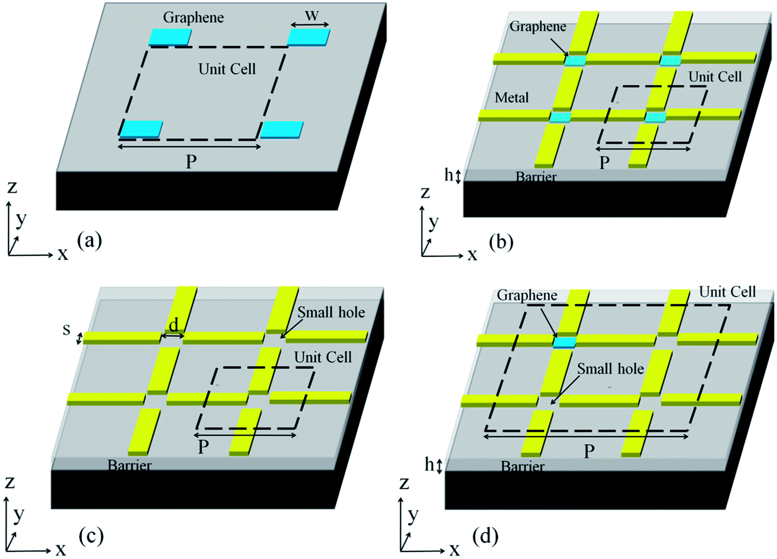 | ||
| Fig. 1 (a) The graphene square structure, (b) the graphene squares with metallic split-meshes structure and (c) the metallic split-meshes structure. (d) Putting 1 graphene square below every 4 small holes. P in (a–d) is the length of a unit cell. | ||
Results and discussion
For the GS structure, the absorption decreases monotonically with increasing the period as shown in Fig. 2(a). The electric field distributions in Fig. 2(c–e) show that the A, B, C and D modes as indicated in Fig. 2(a) are TM(1,0), TM(1,2), TM(3,0) and TM(1,4) mode, respectively. Fig. 2(b) shows that the normalized electric field enhancements |Eloc/E0| of these four modes are nearly fixed at 80, 21, 23 and 10, respectively, where E0 stands for the incident light strength and is normalized to 1. When the period is large enough, the coupling of a single GS with the incident light does not change with increasing the period, so that the field enhancement keeps nearly steady. However, the duty cycle of a GS decreases, resulting in the decreased absorption.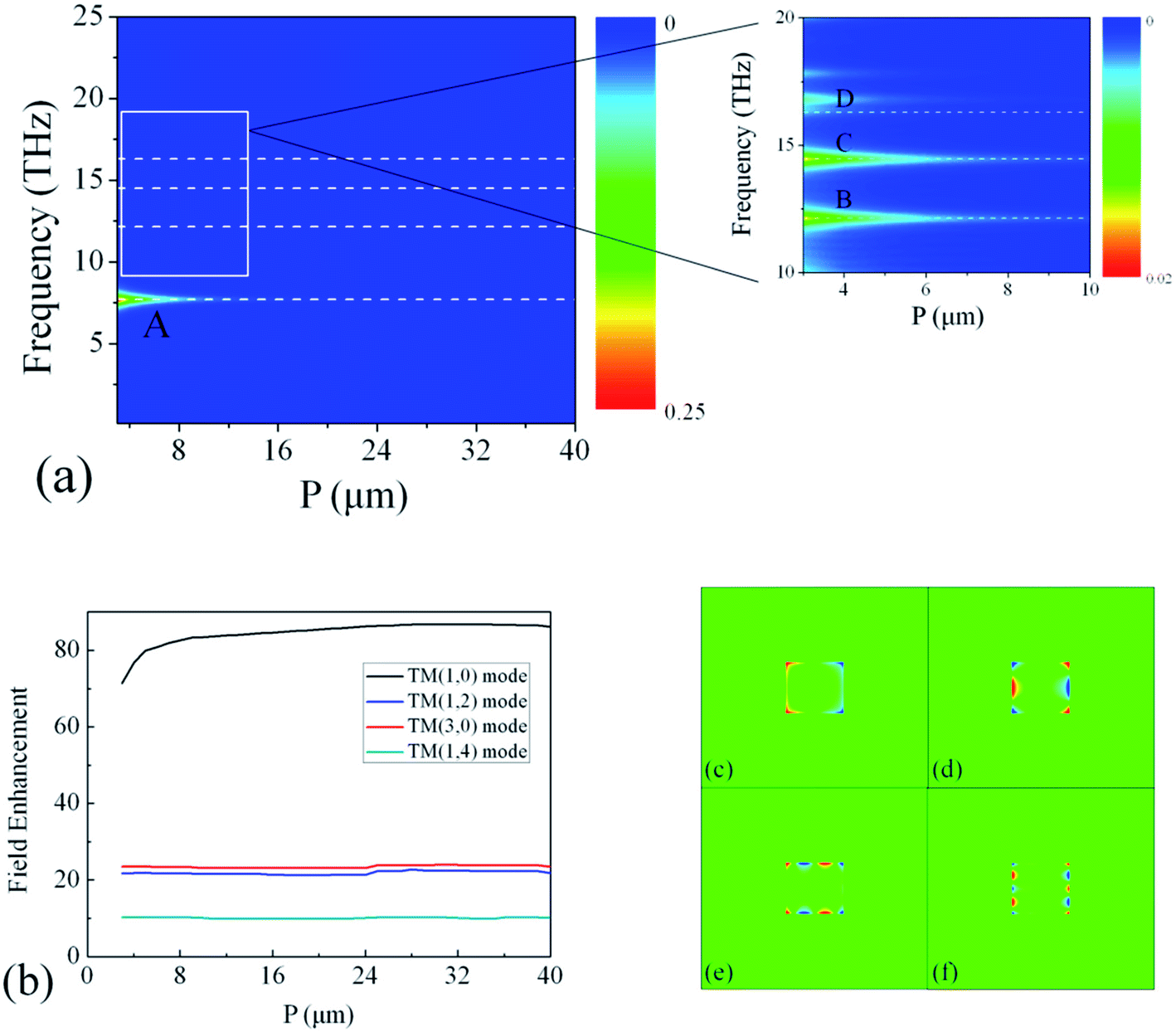 | ||
| Fig. 2 (a) The absorption of the GS structure with the period increasing from 3 μm to 40 μm. (b) The field enhancement of the A, B, C and D mode with the period increasing from 3 μm to 40 μm. (c–f) The Ez distributions corresponding to the A, B, C and D mode as indicated in (a). | ||
By putting MSMs (d = 0.8 μm, s = 0.6 μm) over the GSs with the dielectric separation h = 50 nm, the absorption (shown in Fig. 3(a)) peaks are greatly enhanced, especially for the high order modes which are less than 2% in the GS structure. Because the GS and the MSM structures are isotropic, such enhanced absorption is polarization-independent as shown in Fig. 3(b). The field distributions in Fig. 3(d) show that the A′, B′, C′ and D′ mode as indicated in Fig. 3(a) are also TM(1,0), TM(1,2), TM(3,0) and TM(1,4) mode, respectively. The red-shift of the peaks is due to the attractive coupling between graphene plasmons and the induced charges in metal. The electric field enhancement (Fig. 3(c)) of the GSDMSM structure shows a great improvement of the localized field around the GS. Comparing Fig. 2(b) and 3(c), one can see that the localized fields are greatly raised. The localized field enhancement of the TM(1,0) mode keeps going up with increasing the period and reaches a maximum of 1067 when P = 28 μm and then decreases. The field enhancement of the TM(1,2), TM(3,0) and TM(1,4) mode show alternate increase and decrease.
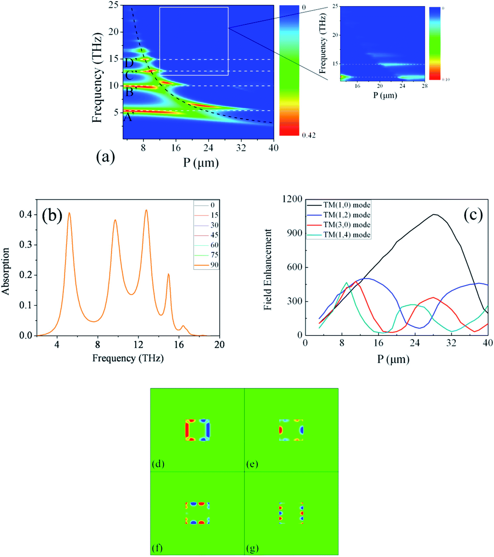 | ||
| Fig. 3 (a) The absorption of the GSDMSM structure with h = 50 nm and increasing P from 3 μm to 40 μm. (b) The absorption of the GSDMSM structure with h = 50 nm, P = 10 μm and different polarization of the incident light. (c) The field enhancement of the A′, B′ C′ and D′ mode with the period increasing from 3 μm to 40 μm. (d–g) The Ez distributions of the A′, B′, C′ and D′ mode, respectively. | ||
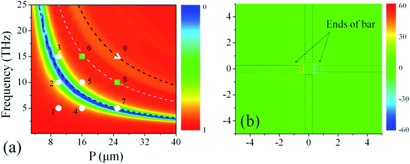
Interestingly, the localized electric fields of all the four graphene plasmon modes, as indicated by the white dashed lines in Fig. 3(a), keep going up before the plasmon modes crossing the black dashed line. When the plasmon modes cross the black dashed line, anti-crossing can be observed. After they anti-cross the black dashed line, they gradually become weak. In Fig. 4(a), the lower black dashed line is the same black dashed line as shown in Fig. 3(a), and is the calculation of the 1st DSP mode of the MSMs with k = π/Leff. The electric field distribution of the dip as shown in Fig. 4(b) also suggests that the dip is caused by the 1st DSP mode of the MSMs. Thus it can be concluded that the transmission dip is caused by the 1st DSP mode. The white dashed line is the calculation of the 2nd DSP mode of the MSMs with k = 2π/Leff and the higher black dashed line is the calculation of the 3rd SPP mode of the MSMs with k = 3π/Leff. As all the plasmon modes will be enhanced within the 1st DSP mode (including its broadening) of the MSMs, the enhancement cannot be explained as the interaction between the graphene plasmon modes and the DSP mode of the MSMs.
 | ||
| Fig. 4 (a) The transmission of the MSM structure with increasing P from 3 μm to 40 μm. (b) The z-component of the electric field of the MSM structure with P = 10 μm at the dip (12.08 THz). | ||
In order to elucidate the physical mechanism that causes the absorption enhancement and the non-enhancement, we study the electric field distribution below the MSM structure corresponding to the points shown in Fig. 4(a). As shown in Fig. 5, for the white points 1–5 and 7, whose corresponding frequencies are lower than or around the frequency of the 1st DSP mode, the z-component of the electric field shows dipole-like distribution at the two ends of the x-directional bars. Under such condition, graphene plasmons interact with the near field and are greatly enhanced. Nevertheless, for the green squares 6 and 8, which correspond to the 2nd DSP mode, the enhanced field will move towards the quadrisection points of the x-directional bar, and the ends of the bars no longer show enhanced field distribution. Therefore, when plasmon modes are heading from the 1st DSP mode to the 2nd DSP mode, the near field at the ends of bars gets weaker and weaker and the absorbance of the plasmon modes is reduced. For the white triangle 9, which corresponds to the 3rd DSP mode, quadrupole DSP mode is excited at the metallic bars and there is again near field enhancement at the metal tips. When plasmon modes are heading from the 2nd DSP mode to the 3rd DSP mode, the near field at the ends of the bars gradually gets stronger and the absorption is enhanced again, as shown in the inset of Fig. 3(a). However, as the ends of bars are not the only region that holds the near field enhancement (the trisection points also hold the near field enhancement), plasmon modes are not enhanced as strong as they are by the dipole-like near field.
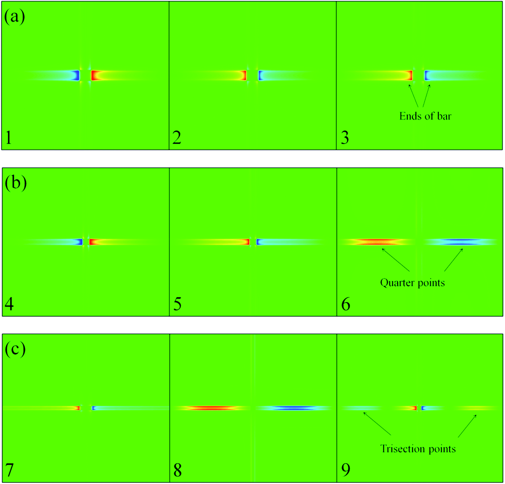 | ||
| Fig. 5 (a) The Ez distributions of the x–y plane at the surface of the metal bar corresponding to the points 1, 2 and 3 in Fig. 4(a). (b) The Ez distributions of the x–y plane corresponding to the points 4, 5 and 6 in Fig. 4(a). (c) The Ez distributions of the x–y plane corresponding to the points 7, 8 and 9 in Fig. 4(a). | ||
It seems in Fig. 3(a) that when P keeps going up, less and less plasmon modes will be enhanced because their frequencies will be higher than that of the 1st DSP mode. However, for conditions with large P, a GS can be put below every 4 small holes instead of every single hole, as schematically shown in Fig. 1(d). For example, for the GS structure with P = 22 μm, depositing the MSM structure with P = 11 μm over the GS with dielectric separation of 50 nm, there will be a GS under every 4 small holes of the MSM structure. Comparing its absorption spectrum with that of the ordinary GSDMSM structure with P = 22 μm, although the absorption of the mixed TM(1,0) and 1st DSP mode is slightly reduced from 41% (taking the mixed mode with higher absorption) to 32% (TM(1,0) mode), the TM(1,2) mode is 34.5% for the former, while the TM(1,2) mode is hardly observed for the latter. According to the absorption equation given in ref. 30, if a device is illuminated from a single side, the absorption can be expressed as
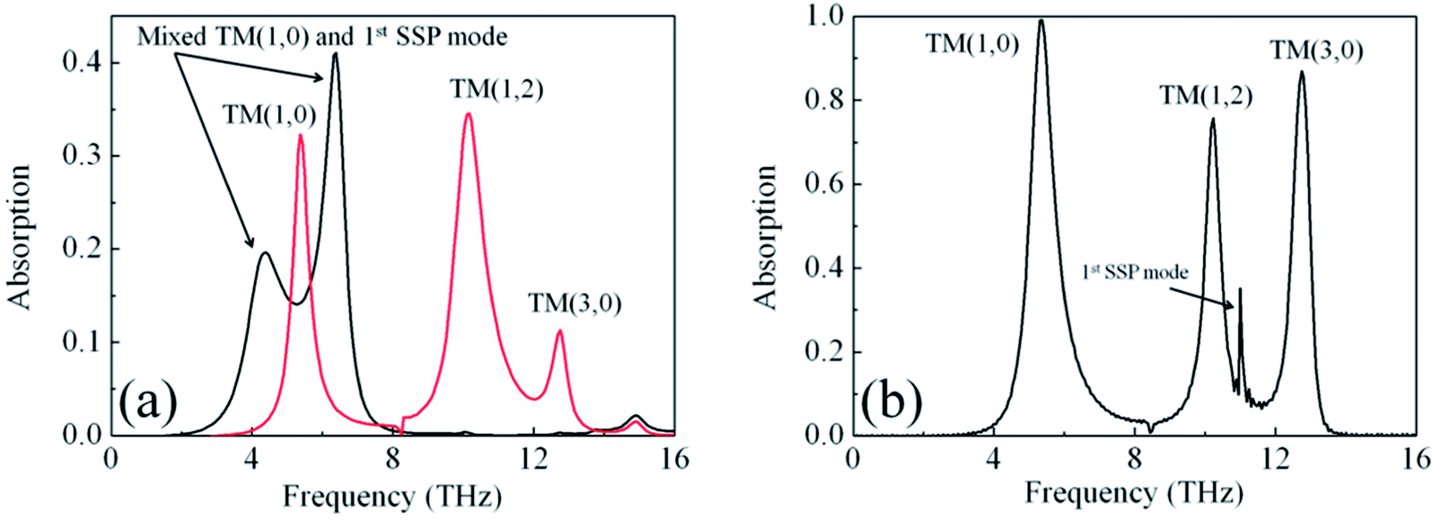 | ||
| Fig. 6 (a) The absorption of putting 1 graphene square below every 4 small holes of the P = 11 μm MSM structure (red curve) and the absorption of the P = 22 μm GSDMSM structure (black curve). (b) The absorption of putting 1 graphene square below every 4 small holes of the P = 11 μm MSM structure and backing the whole structure with a metallic reflector with 7 μm separation. | ||
Conclusion
In conclusion, we apply the MSM structure for enhancing the absorption and the localized electric field of sparse graphene square structure. Such enhancement is polarization-independent because of the isotropy of the GS and the MSM structures. When the frequency of the incident light is lower than the 1st DSP mode of the MSM, dipole-like electric field will be generated at the ends of the metallic bars. The near field at the ends interacts with the graphene plasmons, inducing in great enhancement of the graphene plasmons. To avoid the weakening of the plasmon modes when P is large, we put one graphene square below every 4 small holes of the P/2 MSM structure. A metal back reflector can be put under the graphene squares with appropriate distance to further enhance the absorption and the localized electric field. The results of this work will be helpful for applications with weak THz incidence, such as wireless communication, the detection of cosmic radiations and the identification of macromolecules.Conflicts of interest
There are no conflicts to declare.References
- Y. Feng, Y. Liu, Y. Shi, X. Wang and D. Dong, J. Phys. D: Appl. Phys., 2017, 50, 185101 CrossRef.
- H. Lu, J. Zhao and M. Gu, J. Appl. Phys., 2016, 120, 163106 CrossRef.
- H. Hou, J. Teng, T. Palacios and S. Chua, Opt. Commun., 2016, 370, 226–230 CrossRef.
- X. He, Carbon, 2015, 82, 229–237 CrossRef.
- I. Khromova, A. Andryieuski and A. Lavrinenko, Laser Photonics Rev., 2014, 8, 916–923 CrossRef.
- C. Argyropoulos, Opt. Express, 2015, 23, 23787–23797 CrossRef PubMed.
- S. Das, A. Salandrino, J. Z. Wu and R. Hui, Opt. Lett., 2015, 40, 1516–1519 CrossRef PubMed.
- J. Peng, Z. Zhu, J. Zhang, X. Yuan and S. Qin, Appl. Phys. Express, 2016, 9, 055102 CrossRef.
- Z. Liu and B. Bai, Opt. Express, 2017, 25, 8584–8592 CrossRef PubMed.
- T. Guo and C. Argyropoulos, Opt. Lett., 2016, 41, 5592–5595 CrossRef PubMed.
- Y. Cai, J. Zhu and Q. H. Liu, Appl. Phys. Lett., 2015, 106, 043105 CrossRef.
- S. Xiao, T. Wang, Y. Liu, C. Xu, X. Han and X. Yan, Phys. Chem. Chem. Phys., 2016, 18, 26661–26669 RSC.
- X. Shi, L. Ge, X. Wen, D. Han and Y. Yang, Opt. Express, 2016, 24, 26357–26362 CrossRef PubMed.
- R. Alaee, M. Farhat, C. Rockstuhl and F. Lederer, Opt. Express, 2012, 20, 28017–28024 CrossRef PubMed.
- S. Thongrattanasiri, F. H. L. Koppens and F. J. G. de Abajo, Phys. Rev. Lett., 2012, 108, 047401 CrossRef PubMed.
- R. Parvaz and H. Karami, Opt. Commun., 2017, 396, 267–274 CrossRef.
- G. R. Aizin, V. V. Popov and O. V. Polischuk, Appl. Phys. Lett., 2006, 89, 143512 CrossRef.
- V. V. Popov, Appl. Phys. Lett., 2013, 102, 253504 CrossRef.
- D. V. Fateev, K. V. Mashinsky and V. V. Popov, Appl. Phys. Lett., 2017, 110, 061106 CrossRef.
- Q. Li, Z. Li, X. Chen, P. Chen, X. Shen and W. Lu, Sci. Rep., 2014, 4, 6332 CrossRef PubMed.
- P. J. Zomer, S. P. Dash, N. Tombros and B. J. van Wees, Appl. Phys. Lett., 2011, 99, 232104 CrossRef.
- H. Fischer and O. J. F. Martin, Opt. Express, 2008, 16, 9144–9154 CrossRef PubMed.
- T. Grosjean, M. Mivelle, F. I. Baida, G. W. Burr and U. C. Fischer, Nano Lett., 2011, 11, 1009–1013 CrossRef PubMed.
- B. M. Ross and L. P. Lee, Nanotechnology, 2008, 19, 275201 CrossRef PubMed.
- Y. Zhang, T. Q. Jia, D. H. Feng and Z. Z. Xu, Appl. Phys. Lett., 2011, 98, 163110 CrossRef.
- Y. Zhang, T. Q. Jia, S. A. Zhang, D. H. Feng and Z. Z. Xu, Opt. Express, 2012, 20, 2924–2931 CrossRef PubMed.
- D. M. Sullivan, Electromagnetic simulation using the FDTD method, IEEE Press Series, New York, 2000 Search PubMed.
- A. Taflove, Computational Electromagnetics: The Finite-Difference Time-Domain Method, Artech House, Boston, 2005 Search PubMed.
- S. D. Gedney, Introduction to the Finite-Difference Time-Domain (FDTD) Method for Electromagnetics, Morgen & Claypool publishers, 2011 Search PubMed.
- V. V. Popov, D. V. Fateev, O. V. Polischuk and M. S. Shur, Opt. Express, 2010, 16, 16771–16776 CrossRef PubMed.
| This journal is © The Royal Society of Chemistry 2018 |