DOI:
10.1039/C8RA01569D
(Paper)
RSC Adv., 2018,
8, 13466-13473
Fused silver nanowires with silica sol nanoparticles for smooth, flexible, electrically conductive and highly stable transparent electrodes†
Received
21st February 2018
, Accepted 27th March 2018
First published on 10th April 2018
Abstract
Silver nanowires (AgNWs) thin films have emerged as promising next-generation transparent conductive electrodes (TCEs), and increasing the opto-electrical properties and long-term stability of AgNWs based TCEs is now a major research focus. In this work, a smooth, flexible, electrically conductive and highly stable transparent AgNWs-silica nanoparticles composite TCE has been successfully manufactured via coating an aqueous AgNWs-silica sol composite conductive ink on a PET substrate through the Mayer rod method. The effects of particle size and concentration of silica sol on the smoothness, opto-electrical properties and stability of AgNWs based TCEs were investigated in detail, and the mechanisms of the decoration of AgNWs by silica sol nanoparticles and welding of the network junction are discussed briefly. The TCE based on AgNWs reinforced with 50 nm silica nanoparticles (80 ppm concentration of silica sol) possesses a smooth surface with an RMS value of 9.45 nm, and superior opto-electrical properties with a sheet resistance of 28 Ω sq−1 and a transmittance of 97%. The resistance of the resultant AgNWs-silica composite TCE remains nearly constant after bending for 1000 cycles or exposure to Na2S solution for 300 s, indicating high stability. The newly designed AgNWs-silica composite TCE is a promising flexible and transparent electrode to be applied in next-generation flexible electronic devices.
1. Introduction
In the past decades, the fabrication of flexible and stretchable transparent conductive electrodes (TCEs) has attracted much attention due to their wide use in displays,1 touch screens,2 solar cells,3 and organic light-emitting diodes (OLEDs).4 Up to now, the most commonly used TCE material is indium tin oxide (ITO), which is sputtered on substrates by physical vapor deposition, with the resultant films known to have a high transmittance (over 90%) and a low sheet resistance (under 30 Ω sq−1).5 However, ITO film is not suitable for flexible applications and large area applications because of its high brittleness, high cost, and complicated processing conditions.6 The rapid development of new electronic devices is creating a demand for novel materials to replace ITO. A variety of candidates have been developed including conducting polymers,7 graphene,8 carbon nanotubes,9 and their hybrids. Among them, silver nanowires (AgNWs) are among the most promising candidates due to their excellent conductivity, superior optical properties, flexibility and compatibility with large-scale manufacturing.10–16
Great improvements have been made by researchers around the world for AgNWs based TCEs.17–22 However, there remain several issues to be addressed for the practical commercialization of AgNWs based TCEs. Firstly, the high contact resistance at nanowire–nanowire (NW–NW) junctions greatly limits the current delivery capability of AgNWs thin films. At present, AgNWs can be easily synthesized using the well-established polyol reduction method in the presence of polyvinylpyrrolidone (PVP),23–25 but the residual PVP ligands will form an insulating layer around the AgNWs, resulting in high contact resistance at NW–NW junctions. A number of strategies have been developed to improve the conductivity of AgNWs thin films, including mechanical pressing,26,27 plasmonic welding,10,28 thermal annealing,27,29,30 adding soldering agents,31–33 capillary-force-induced cold welding,34 nanowire assembly,2,35 and photochemical welding.36,37 However, these strategies either need harsh conditions or are not efficient enough for large area fabrication. For example, mechanical pressing cannot be applied to some devices as the high pressure may destroy some useful structures or the active layer. Thermal annealing has the risk of damaging the flexible host substrate (e.g., polyethylene glycol terephthalate, PET). Secondly, the poor long-term stability of AgNWs is also highly problematic. AgNWs are easily oxidized in humid air due to their interactions with moisture, oxygen, and especially sulfur-containing compounds.33 To solve this problem, a variety of materials have been exploited as the protective layer. Ge et al.38 decorated the as-formed AgNWs thin films with a dense, hydrophobic dodecanethiol layer and the stability of the AgNWs thin film was greatly improved by 150 times compared with that of PVP-wrapped ones. Lee6 introduced an indium-doped zinc oxide (IZO) buffer layer onto AgNWs thin films, which protected the AgNWs from surface oxidation and improved the mechanical and chemical stability of the composite film. Lee39 developed an AgNWs-graphene hybrid electrode by dry-transferring a CVD-grown monolayer graphene onto an AgNWs network, which showed highly enhanced thermal oxidation and chemical stabilities due to the gas-barrier effect of the graphene layer. Although the stability of AgNWs TCEs can clearly be improved with the use of an active layer, the fabrication process involves two or more sequential steps and needs to be precisely controlled, which is not convenient for the commercialization of AgNWs based TCEs. Therefore, it still remains a challenge to develop a highly efficient approach that can be applied under mild conditions over a large scale to simultaneously improve both the conductivity and stability of AgNWs thin films.
In this work, AgNWs with a diameter of 40 nm were firstly synthesized by the polyol reduction method, and then an aqueous conductive composite ink was prepared using AgNWs as conductive material, silica sol as reinforcing additive, the fluorocarbon surfactant Zonyl FSO-100 as surface modifier and hydroxypropyl methylcellulose (HPMC) as adhesive. Finally, flexible TCEs with size of 30 × 30 cm2 were fabricated on PET substrates by the Mayer rod method. Silica sol nanoparticles can easily aggregate onto AgNWs, because this minimizes their free energy. Like with other nanoparticles (such as TiO2 sol40 and SiO2 hollow nanospheres41), the volume shrinkage of silica sol nanoparticles and the capillary force induced by solvent evaporation can bind AgNWs together, thus decreasing the contact resistance between NWs and improving the film conductivity. Furthermore, the silica sol nanoparticles on the surface of AgNWs can act as a gas-barrier, like galvanic gold,42 to enhance the long-term stability of the AgNWs based TCE and fill the gaps between AgNWs to form a smooth surface. The fabricated AgNWs-silica composite TCE shows a transmission of 97%, a sheet resistance of 28 Ω sq−1, a root mean square (RMS) roughness value of 9.45 nm and high stability after bending for 1000 cycles or exposure to Na2S solution for 300 s, making it a promising alternative to conventional ITO films in next generation flexible electronic devices.
2. Experimental
2.1 Starting materials
AgNO3 (99.8%, Sinopharm Chemical Reagent Co., Ltd.) and ethylene glycol (EG, 98.0%, Aladdin Industrial Corporation) were used as the source material and the reductant respectively. Two forms of PVP (one with an average Mw of 58![[thin space (1/6-em)]](https://www.rsc.org/images/entities/char_2009.gif) 000, named PVP-58000, Aladdin Industrial Corporation, the other with an average Mw of 360000, named PVP-360000, Sigma-Aldrich) were used as capping agents. Anhydrous FeCl3 (98.0%, Aladdin Industrial Corporation) was used as a nucleating agent. HPMC (Sinopharm Chemical Reagent Co., Ltd.), fluorocarbon surfactant (Zonyl FSO-100, DuPont) and aqueous ammonia (25%, Sinopharm Chemical Reagent Co., Ltd.) were used for AgNWs ink formation before film coating. Silica sol (4 nm, 10% of solid content, self-made by the Stöber method), silica sol (8 nm, 30% of solid content, Guangzhou Suize Environmental Protection Technology Co., Ltd.) and silica sol (50 nm, 50% of solid content, Shanghai Huipu Industrial Chemicals Co., Ltd.) were used as reinforcing agents for AgNWs based TCEs. PET (0.125 mm thickness, Dongguan Shouyu Electronic Materials Co., Ltd.) was used as a flexible substrate. Ethanol (AR, Sinopharm Chemical Reagent Co., Ltd), acetone (AR, Sinopharm Chemical Reagent Co., Ltd) and ultrapure water (self-made) were used throughout the experiments.
000, named PVP-58000, Aladdin Industrial Corporation, the other with an average Mw of 360000, named PVP-360000, Sigma-Aldrich) were used as capping agents. Anhydrous FeCl3 (98.0%, Aladdin Industrial Corporation) was used as a nucleating agent. HPMC (Sinopharm Chemical Reagent Co., Ltd.), fluorocarbon surfactant (Zonyl FSO-100, DuPont) and aqueous ammonia (25%, Sinopharm Chemical Reagent Co., Ltd.) were used for AgNWs ink formation before film coating. Silica sol (4 nm, 10% of solid content, self-made by the Stöber method), silica sol (8 nm, 30% of solid content, Guangzhou Suize Environmental Protection Technology Co., Ltd.) and silica sol (50 nm, 50% of solid content, Shanghai Huipu Industrial Chemicals Co., Ltd.) were used as reinforcing agents for AgNWs based TCEs. PET (0.125 mm thickness, Dongguan Shouyu Electronic Materials Co., Ltd.) was used as a flexible substrate. Ethanol (AR, Sinopharm Chemical Reagent Co., Ltd), acetone (AR, Sinopharm Chemical Reagent Co., Ltd) and ultrapure water (self-made) were used throughout the experiments.
2.2 AgNWs synthesis
AgNWs were synthesized through a modified polyol process as follows. 1.0 g PVP-58000 and 2.0 g PVP-360000 were dissolved in 450 mL EG and transferred into a glass vial with a stir bar, and the vial was then suspended in an oil bath (temperature 140 °C) and heated for 1 h under magnetic stirring (300 rpm). Concurrent to this heating, the reagent solutions were prepared. At 1 h, 50 mL of FeCl3 (600 μM in EG) and 60 mL of AgNO3 solution (3.6 g in EG) were added rapidly into PVP solution within 5 min. The reaction was performed at 140 °C for 50 min. After cooling to room temperature, the solution was washed with ethanol, centrifuged and dispersed in ethanol. The purification process was repeated 3 times. A final dispersion of AgNWs in ethanol (5 mg mL−1) was obtained.
2.3 Conductive ink preparation and TCEs fabrication
To achieve AgNWs-silica composite TCEs, AgNW-based ink was prepared firstly with the following procedure: AgNWs (1.4 mg mL−1), silica sol (concentration: 80 ppm, nanoparticle size: 4, 8 and 50 nm), HPMC (3.2 mg mL−1), Zonyl FSO-100 (1 mg mL−1), and aqueous ammonia (5 mg mL−1) were the reactants and ultrapure water was the solvent. An automatic coating machine (FA 202D, Shanghai Xianpu Industrial Co., Ltd.) equipped with a Mayer rod was utilized to coat AgNWs ink on PET substrates, and the coating rate and area were fixed at 1 mm s−1 and 30 × 30 cm2, respectively. The starting button was pressed after dropping 2.5 mL of AgNWs ink and the obtained AgNWs-silica composite TCEs were placed on the platform for further 5 min to allow the evaporation of solvent under ambient conditions.
2.4 Characterization
Scanning electron microscopy (SEM) images of the as-prepared AgNWs and composite TCEs were obtained with an SU8010 high resolution microscope with an accelerating voltage of 3 kV. Transmission electron microscopy (TEM) images were observed with a JEOL JEM-1230 instrument. Atomic force microscopy (AFM) images were achieved with a Veeco instrument. Powder X-ray diffraction (XRD) patterns were recorded with a Shimadzu XRD-6000 diffractometer (Cu Kα radiation; 40 kV, 60 mA). The sheet resistance of the AgNWs-silica composite TCEs was measured with a four-probe surface resistivity meter (RTS-9, Guangzhou Four-point Probe Technology). Transmittance spectra were performed with a UV-Vis spectrophotometer (DU800, Beckman) with the PET substrates as a reference.
3. Results and discussion
Fig. 1A shows the SEM images of AgNWs. The nanowires with diameter of 40 nm and length of 25 μm can be recognized in the images. Fig. 1B depicts the XRD pattern of the uniform AgNWs. All the diffraction peaks can be indexed to the (111), (200), (220) and (311) planes of pure face-centered cubic (fcc) silver crystal, and are consistent with the standard values according to JCPDS Card No. 04-0783.43 No impurities are detected, indicating the formation of highly pure AgNWs. Fig. 1C shows the HRTEM image of typical AgNWs, revealing the nanowires to be highly crystalline with an estimated spacing of 0.236 nm for adjacent lattice planes, which corresponds to the (111) planes of face-centered silver. The selected-area electron diffraction (SAED) pattern demonstrates that the silver nanowires have a fivefold twinned crystal structure, and the site tested corresponds to the region indicated by the square in Fig. 1C. This pattern typically consists of two sets of spots corresponding to either side of the nanowires, and represents the characteristic reflection twins in an fcc metal and displays the reflection symmetry about the (111)-type plane.44 Fig. 1D presents the extinction spectrum of AgNWs suspension in ethanol. It can be observed that AgNWs suspension shows two absorption peaks. The origin of the left peak located at ca. 350 nm is attributed to quadruple resonance, while the right peak located at ca. 377 nm originates from the dipole resonance, which has a sensitive variation law with the dimensions of silver nanostructures. Both peaks originate from the transverse plasmon resonance modes of nanowires, which are associated with the pentagonal cross-section shape of AgNWs.25
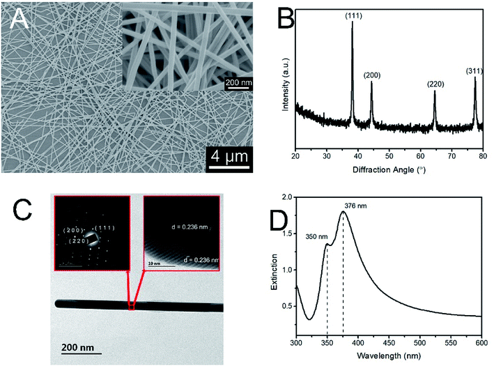 |
| | Fig. 1 (A) SEM images of AgNWs; (B) XRD pattern of AgNWs; (C) HR-TEM image of AgNWs; (D) UV-Vis absorption of AgNWs. | |
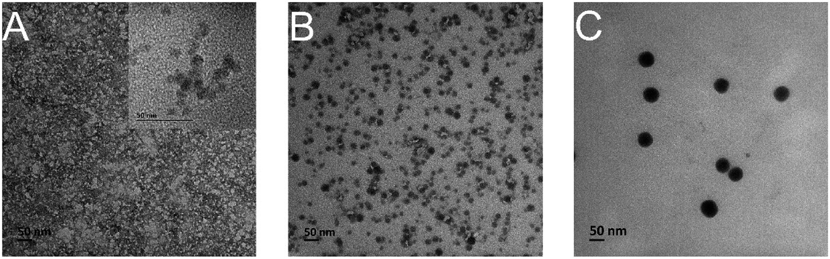
Fig. 2A shows the TEM image of 4 nm silica sol nanoparticles obtained by the Stöber method using Si(OC2H5)4 as the starting material.45 Fig. 2B and C are TEM images of 8 and 50 nm silica, both of which were produced via hydrolyzation of sodium silicate solution followed by an ion exchange process. It can be seen that all three sol nanoparticles are spherical with a uniform particle size distribution. In contrast, the silica sol becomes less well dispersed with the decrease of particle size.
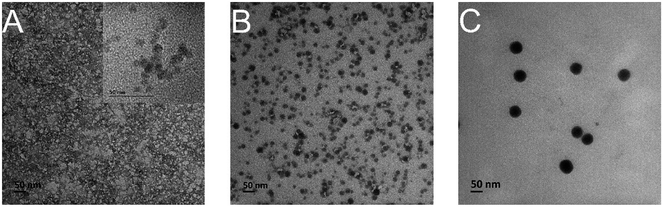 |
| | Fig. 2 TEM images of silica sol nanoparticles with different diameters, (A) 4 nm, (B) 8 nm, (C) 50 nm. | |
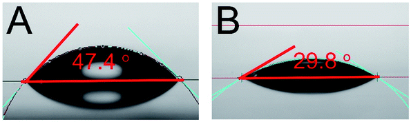
As is well known, there are three steps in the preparation of AgNWs based TCEs: synthesis of AgNWs, preparation of conductive ink and fabrication of TCEs. As a bridge between AgNWs and TCEs, conductive ink is responsible for the control of many dynamic processes such as the stabilization of AgNWs, as well as the wetting, spreading and drying of the films. Therefore, high-quality inks usually contain many additives to allow fine adjustment of these dynamic processes.46 In this study, AgNWs inks are prepared with the following starting materials: AgNWs, silica sol, HPMC, Zonyl FSO-100, aqueous ammonia and ultrapure water. Among these additives, water soluble and eco-friendly HPMC is used as the viscosity modifier and film-forming agent for AgNW inks.47 Without HPMC, AgNWs will aggregate during the drying process as shown in Fig. S1 in the ESI,† resulting in inhomogeneous distribution and high sheet resistance of over 1 kΩ sq−1. Water is chosen as the solvent of this ink, and it has a high surface tension of 72.25 mN m−1, which is much higher than that of typical flexible substrates (about 40 mN m−1). According to the Young equation,45 if the surface tension of the ink is higher than that of the substrate, the ink will have bad wettability with the substrate, which means that when the ink is put on the substrate, it will maintain a globular morphology that brings about very bad uniformity.46 To solve this problem and ensure that the ink has good wettability, that is, that the ink can spread over the substrate, it is necessary to adjust the ink to make its surface tension lower than that of the substrate. Zonyl FSO-100,46,47 used as an efficient liquid fluorocarbon surfactant, can adjust the surface tension of the ink. Fig. 3A demonstrates that the ink without Zonyl FSO-100 shows a contact angle of 47.4°, while the contact angle of the ink drops to 29.8° after the addition of Zonyl FSO-100, which is satisfactory for spreading over PET substrates. AgNWs are easily aggregated in deionized water, especially after the introduction of silica sol.41 Two methods are most commonly used to prevent the nanomaterials' aggregation: the steric effect and electrostatic repulsion.46 The steric effect is usually introduced using polymers, but these can easily adhere to the material surface and result in high sheet resistance of AgNWs based TCEs. Thus, in this ink, we adjusted the electrostatic repulsion between AgNWs with the addition of aqueous ammonia to the ink, leading to the fabrication of a composite ink with higher stability, even after storing for several months. According to a previous study,48 the zeta potentials of AgNW and silica sol are negatively charged in fabricated inks. The addition of aqueous ammonia to the ink will increase the pH, which makes the AgNWs and silica sol surfaces more negative and hence results in higher repulsive force, bringing about higher stability for the AgNW ink.46
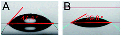 |
| | Fig. 3 The contact angles of AgNWs conductive inks with (A) and without (B) surfactant, (A) 47.4°; (B) 29.8°. | |
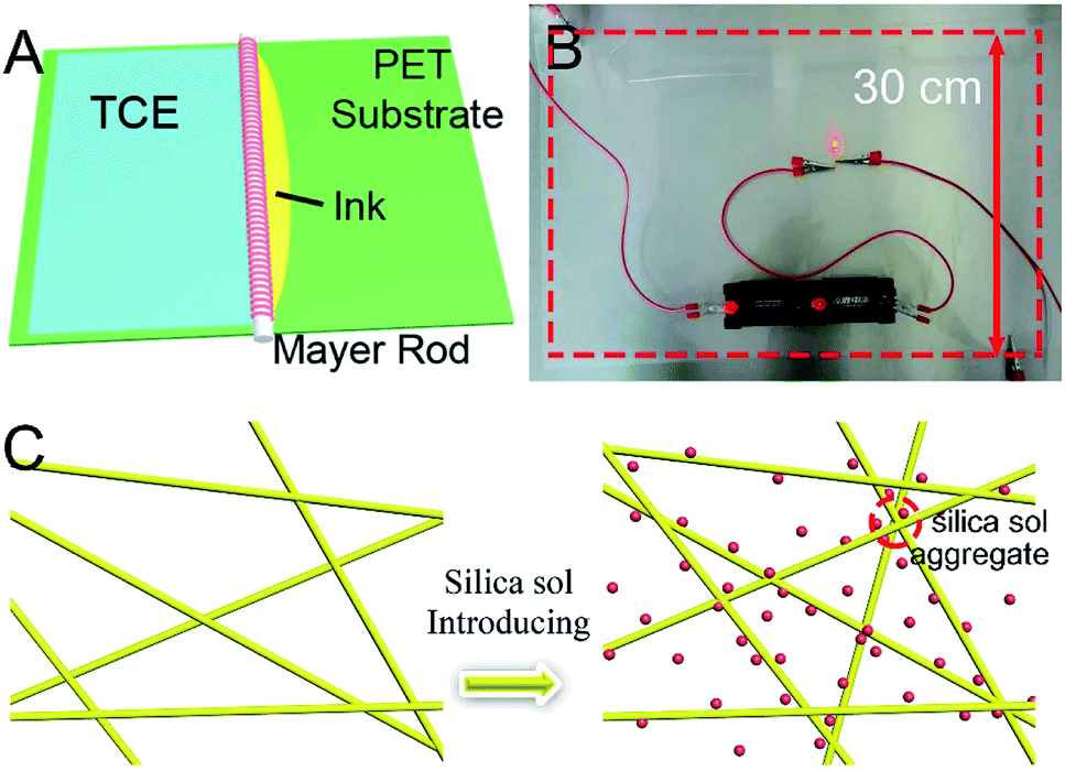
After preparation of AgNWs ink, AgNW based TCEs with 30 × 30 cm2 areas were fabricated on PET substrates via the Mayer rod coating process, depicted in Fig. 4A. In brief, 2.5 mL AgNWs ink is dipped onto the PET substrate along the Mayer rod direction, and then the Mayor rod slides and spreads the ink over the substrates. After the evaporation of solvent, a uniform AgNW network on PET substrate is formed (Fig. 4B). The AgNWs are only weakly connected to each other due to the residual PVP, leading to high sheet resistance. In this work, silica sol is used as a room-temperature fusing agent to strengthen the connection between AgNWs. The volume shrinkage of silica sol and the capillary force induced by solvent evaporation act to bind AgNWs together, thus decreasing the contact resistance between NWs and improving the film conductivity (Fig. 4C).
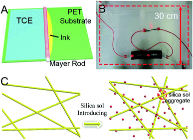 |
| | Fig. 4 (A) Schematic diagram of the procedure for fabricating TCEs, (B) photograph of a large-scale (30 cm × 30 cm) flexible TCE, (C) schematic presentation of introduction of silica sol onto the surface of AgNWs. | |
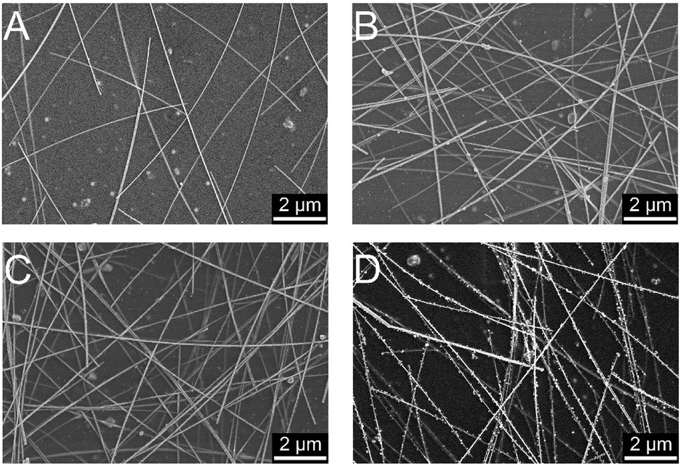
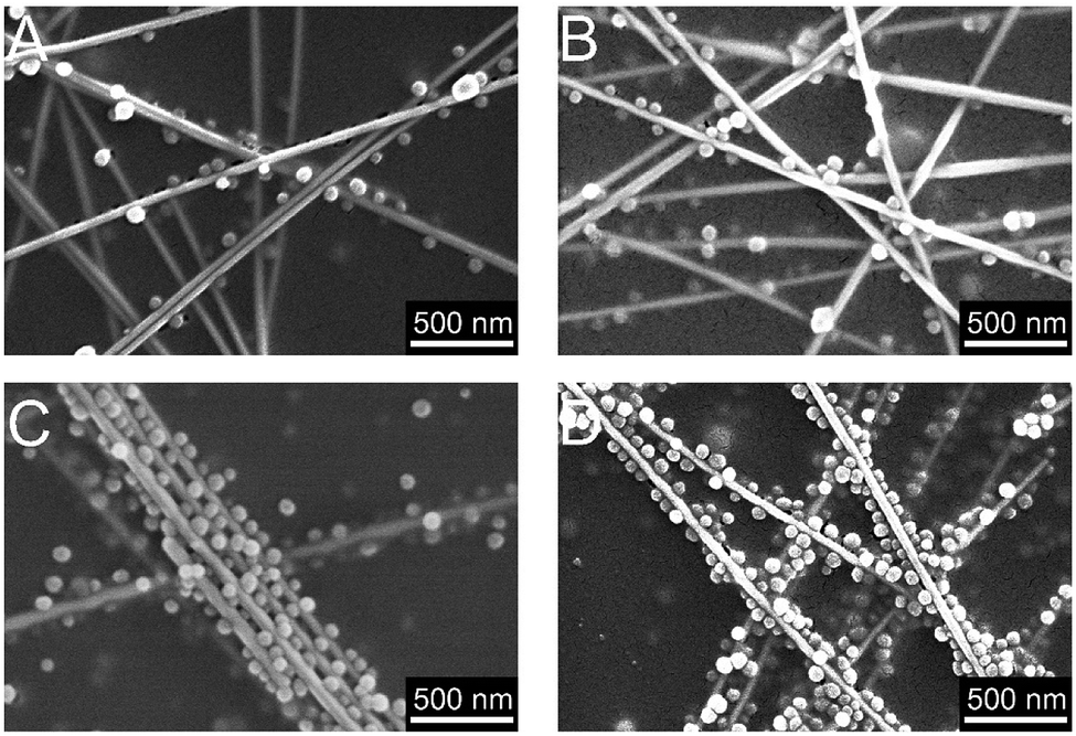
Fig. 5 shows the SEM images of AgNWs-silica composite TCEs with different nanoparticle sizes of silica sol. It is notable that the silica nanoparticles are mainly decorated around the AgNWs, as this configuration minimizes their free energy. The AgNWs based TCE without silica sol has a transmittance of 98% and a sheet resistance of 62 Ω sq−1. After adding 4 nm silica sol, the opto-electrical properties do not change noticeably. After replacing 4 nm silica sol with 8 nm silica sol, the sheet resistance decreases to 36 Ω sq−1, and it then further decreases to 28 Ω sq−1 (transmittance of 97%) when replacing 8 nm silica sol with 50 nm silica sol. This decrease may be ascribed to the greater volume shrinkage caused by bigger silica nanoparticles, thus leading to stronger connection between AgNWs. Fig. 6 shows the SEM images of AgNWs-silica composite TCEs with varied concentrations of silica sol (50 nm nanoparticle size). The silica sol can bind the AgNWs together, but it still has an adverse effect on the opto-electrical properties of AgNWs due to its nonconductive properties. When the concentration of silica sol is 40 ppm, very few silica nanoparticles are decorated on the AgNWs, thus, a slightly decreased sheet resistance of 57 Ω sq−1 is achieved compared to the pristine AgNWs based TCE. When the concentration of silica sol is 80 ppm, silica nanoparticles are uniformly decorated on the AgNWs, and a sheet resistance as low as 28 Ω sq−1 can be obtained. When the concentration of silica sol increases to 120 ppm, the adverse effects of silica sol are apparent with abundant nonconductive silica particles aggregated on the AgNWs junctions, leading to a sheet resistance of 75 Ω sq−1. It is seen from Fig. 6D that the AgNWs-silica composite TCE with 200 ppm silica sol shows the complete decoration of the AgNWs with silica nanoparticles, resulting in a sheet resistance over 1 kΩ sq−1.
 |
| | Fig. 5 SEM images of AgNWs-silica composite TCEs: without silica sol (A), with 4 nm (B), 8 nm (C) and 50 nm (D) silica sols. | |
 |
| | Fig. 6 SEM images of AgNWs-silica composite TCEs with varied concentrations of 50 nm silica sol, (A) 40 ppm, (B) 80 ppm, (C) 120 ppm, (D) 200 ppm. | |
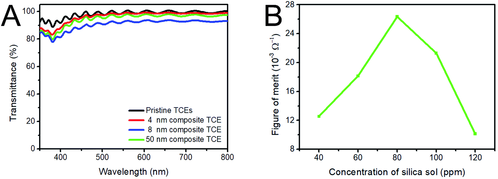
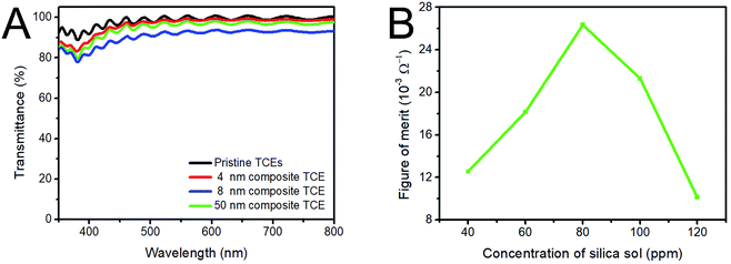
The introduction of silica sol also has effects on the transmittance of AgNWs based TCEs, as shown in Fig. 7A. 4 nm silica sol nanoparticles have no obvious effect on the opto-electrical properties of AgNWs based TCEs, although they aggregate on the AgNWs surface. For 8 nm silica sol nanoparticles, when the concentration of silica sol increases to 80 ppm, the AgNWs ink contains a huge number of nanoparticles with diameter of 8 nm, which fully decorate the surface of the AgNWs, affording AgNWs with larger diameter. According to previous research,49–51 the transmittance of TCEs is related to the area coverage Ac as shown in eqn (1) and (2). Therefore, with increasing diameter of AgNWs, the Ac increases, and the transmittance decreases. For 50 nm silica sol nanoparticles, at the same concentration as 8 nm silica sol, the amount of particles is much less than that of 8 nm silica sol, which prevents the particles from fully decorating the AgNWs to increase their diameter. Therefore, the transmittance decreases slightly compared to that of the pristine AgNWs based TCE.
where
N is the number of AgNWs,
L is the length of AgNWs,
d is the diameter of the AgNWs and
T is the transmittance of TCEs.
 |
| | Fig. 7 (A) Transmittance spectra with different particle sizes of silica sol, (B) ΦTC values with different concentrations of 50 nm silica sol nanoparticles. | |
For in-depth analysis of the AgNW-silica composite TCEs, the figure-of-merit (ΦTC) defined by Haacke52,53 is used to evaluate the quality of the TCEs. The ΦTC is related to the transmittance (T) and the sheet resistance (RS) of TCEs, as shown in the following eqn (3):
| |
 | (3) |
As mentioned above, 50 nm silica sol nanoparticles have an obvious effect on the transmittance and sheet resistance of the AgNWs-silica composite TCEs. As their concentration increases from 0 to 120 ppm, the resulting AgNWs show the largest ΦTC of 26 × 10−3 Ω−1 at a silica sol concentration of 80 ppm (Fig. 7B).
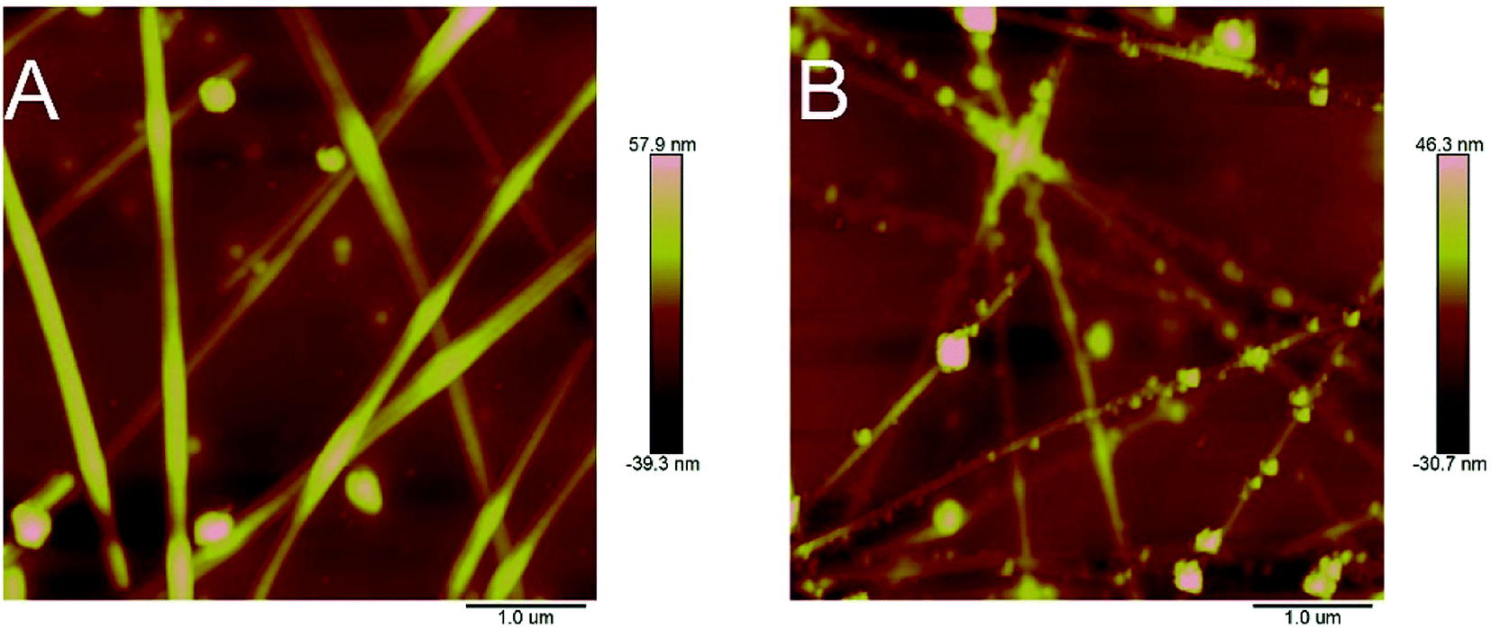
Fig. 8 exhibits the AFM images of the AgNWs-silica composite TCEs, and demonstrates that the AgNWs-silica composite TCE with 50 nm silica sol nanoparticles has an RMS value of 9.45 nm, lower than that of the pristine TCE (14.1 nm). 50 nm silica sol nanoparticles have the same size as the diameter of AgNWs, allowing these nanoparticles to fill the gap between AgNWs efficiently. As is known, the RMS value of AgNWs has dramatic effects on their application.54,55 The present results indicate that the low RMS value of the AgNWs based composite TCE with 50 nm silica sol nanoparticles makes it a good alternative candidate to ITO for use in touch screens or OLEDs.
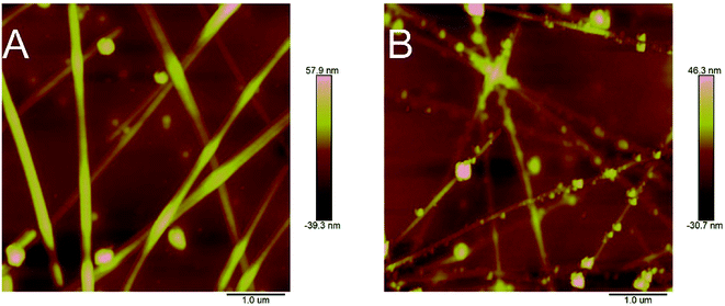 |
| | Fig. 8 AFM observation of the morphology changes of AgNWs based TCE. (A) without silica sol; (B) composite with 50 nm silica sol nanoparticles. | |
Weak adhesion to substrates and poor chemical resistance to oxidation or sulfurization are the main issues of AgNWs-silica composite TCEs.46,47 Fig. 9 shows that the AgNWs based TCE with 50 nm silica sol nanoparticles has no change in sheet resistance after bending for 1000 cycles, which is attributed to the addition of HPMC and silica sol. HPMC is a binder to provide strong adhesion to substrates, and silica sol can improve the adhesion between substrates and AgNWs.41 The AgNWs TCE with 50 nm silica sol also has strong chemical resistance against oxidation: after exposure in atmospheric environment for 30 days, its opto-electrical properties remain almost constant. The same results were obtained when the AgNWs TCE was exposed to H2S gas for 24 h. However, the AgNWs based composite TCE without silica sol became black after exposure to H2S gas for 6 h, and the transmittance decreased to 60%. This demonstrated that the synergistic gas-barrier effects of HPMC and silica sol are important to improve the chemical resistance of AgNWs based TCEs. In this study, the AgNWs-silica composite TCEs were dipped into 5 wt% Na2S solution for chemical resistance testing. It is seen from Fig. 10A that the AgNWs based TCE with 50 nm silica sol nanoparticles shows nearly the same sheet resistance after 300 s immersion. In contrast, for the pristine AgNWs based TCE without silica sol, its sheet resistance obviously increases after 300 s immersion. HPMC is soluble in water, so that when the AgNWs-silica composite TCEs are immersed into Na2S solution, the HPMC will quickly dissolve in water, meaning that the bare AgNWs come into direct contact with Na2S to form Ag2S impurities. By comparison, silica sol provides another barrier between AgNWs and Na2S after the disappearance of HPMC, so the AgNWs TCE with 50 nm silica sol nanoparticles is more stable in Na2S solution. This conclusion is also confirmed in Fig. 10B. After immersion in Na2S solution for 300 s, the AgNWs based TCE without silica sol is destroyed completely with no visible AgNWs, while for the AgNWs-silica composite TCE with 50 nm silica sol nanoparticles, some AgNWs still survive and form connections.
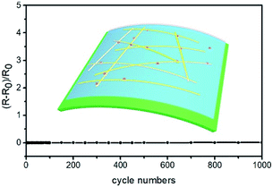 |
| | Fig. 9 Variation in resistance of TCEs after repeated tensile bending test.56 | |
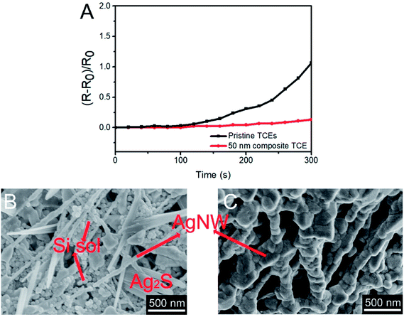 |
| | Fig. 10 (A) Variation in resistance of TCEs after immersion into Na2S solution; (B) SEM images of silica sol reinforced AgNWs-silica composite TCE after immersion into Na2S solution for 300 s; and (C) TCE without silica sol. | |
4. Conclusions
Silver nanowires based transparent conductive electrodes (AgNWs based TCEs) were successfully manufactured through three steps: AgNWs synthesis, conductive ink preparation and TCE fabrication. The AgNWs with diameter of 40 nm and length of 25 μm can be easily synthesized by a modified polyol process. The preparation of the stable and easily-processed AgNWs inks depends on the addition of HPMC, Zonyl FSO-100 surfactant and aqueous ammonia. AgNWs based TCEs were simply fabricated on a large scale on PET substrates via the Mayer rod coating process. After the addition of silica sol into AgNWs conductive inks, the sol nanoparticles spontaneously aggregated onto the AgNWs surface to decorate the AgNWs through volume shrinkage and capillary force, and the silica sol particle size and concentration played an important role in the opto-electrical properties of the as-fabricated AgNWs-silica composite TCEs. The TCE based on AgNWs reinforced by 50 nm silica sol nanoparticles (80 ppm concentration) possesses the best opto-electrical properties: its sheet resistance reaches 28 Ω sq−1, the transmittance is 97% at 550 nm, and the RMS value is 9.45 nm. This AgNWs-silica composite TCE shows a high stability, and its sheet resistance remains nearly constant after bending for 1000 cycles or exposure to Na2S solution for 300 s, indicating high stability. The newly designed silica sol reinforced AgNWs-silica composite TCE is a promising alternative to conventional ITO films for the production of flexible and transparent electrodes to be applied in next-generation flexible electronic devices.
Conflicts of interest
There are no conflicts to declare.
Acknowledgements
This work is supported by the National Key Research and Development Program (2016YFB0401305).
References
- J. Zhang, C. Wang and C. Zhou, ACS Nano, 2012, 6, 7412–7419 CrossRef CAS PubMed.
- S. Cho, S. Kang, A. Pandya, R. Shanker, Z. Khan, Y. Lee, J. Park, S. L. Craig and H. Ko, ACS Nano, 2017, 11, 4346–4357 CrossRef CAS PubMed.
- F. Selzer, N. Weiss, D. Kneppe, L. Bormann, C. Sachse, N. Gaponik, A. Eychmueller, K. Leo and L. Mueller-Meskamp, Nanoscale, 2015, 7, 2777–2783 RSC.
- L. Li, Z. Yu, W. Hu, C. Chang, Q. Chen and Q. Pei, Adv. Mater., 2011, 23, 5563 CrossRef CAS PubMed.
- H. Kim, C. M. Gilmore, A. Pique, J. S. Horwitz, H. Mattoussi, H. Murata, Z. H. Kafafi and D. B. Chrisey, J. Appl. Phys., 1999, 86, 6451–6461 CrossRef CAS.
- H. J. Lee, J. H. Hwang, K. B. Choi, S. Jung, K. N. Kim, Y. S. Shim, C. H. Park, Y. W. Park and B. Ju, ACS Appl. Mater. Interfaces, 2013, 5, 10397–10403 CAS.
- H. Wang, P. Cheng, Y. Liu, J. Chen, X. Zhan, W. Hu, Z. Shuai, Y. Li and D. Zhu, J. Mater. Chem., 2012, 22, 3432–3439 RSC.
- S. Bae, H. Kim, Y. Lee, X. Xu, J. Park, Y. Zheng, J. Balakrishnan, T. Lei, H. Ri Kim, Y. I. Song, Y. Kim, K. S. Kim, B. Özyilmaz, J. Ahn, B. H. Hong and S. Iijima, Nat. Nanotechnol., 2010, 5, 574–578 CrossRef CAS PubMed.
- B. S. Shim, J. Zhu, E. Jan, K. Critchley and N. A. Kotov, ACS Nano, 2010, 4, 3725–3734 CrossRef CAS PubMed.
- E. C. Garnett, W. Cai, J. J. Cha, F. Mahmood, S. T. Connor, M. Greyson Christoforo, Y. Cui, M. D. McGehee and M. L. Brongersma, Nat. Mater., 2012, 11, 241–249 CrossRef CAS PubMed.
- J. Gao, K. Kempa, M. Giersig, E. M. Akinoglu, B. Han and R. Li, Adv. Phys., 2016, 65, 553–617 CrossRef CAS.
- F. Xu and Y. Zhu, Adv. Mater., 2012, 24, 5117–5122 CrossRef CAS PubMed.
- P. Lee, J. Lee, H. Lee, J. Yeo, S. Hong, K. H. Nam, D. Lee, S. S. Lee and S. H. Ko, Adv. Mater., 2012, 24, 3326–3332 CrossRef CAS PubMed.
- Z. Yu, Q. Zhang, L. Li, Q. Chen, X. Niu, J. Liu and Q. Pei, Adv. Mater., 2011, 23, 664–668 CrossRef CAS PubMed.
- M. Cao, M. Wang, L. Li, H. Qiu and Z. Yang, ACS Appl. Mater. Interfaces, 2018, 10, 1077–1083 CAS.
- H. Sohn, S. Kim, W. Shin, J. M. Lee, H. Lee, D. Yun, K. Moon, I. T. Han, C. Kwak and S. Hwang, ACS Appl. Mater. Interfaces, 2018, 10, 2688–2700 CAS.
- B. Li, S. Ye, I. E. Stewart, S. Alvarez and B. J. Wiley, Nano Lett., 2015, 15, 6722–6726 CrossRef CAS PubMed.
- G. Huang, H. Xiao and S. Fu, Nanoscale, 2014, 6, 8495–8502 RSC.
- S. J. Lee, Y. Kim, J. K. Kim, H. Baik, J. H. Park, J. Lee, J. Nam, J. H. Park, T. Lee, G. Yi and J. H. Cho, Nanoscale, 2014, 6, 11828–11834 RSC.
- M. B. Gebeyehu, Y. Chang, A. K. Abay, S. Chang, J. Lee, C. Wu, T. Chiang and R. Murakami, RSC Adv., 2016, 6, 54162–54168 RSC.
- D. Kim, H. Shin, E. Ko, K. Kim, T. Kim and H. Kim, Sci. Rep., 2016, 6, 34322 CrossRef CAS PubMed.
- N. Zhang, X. Yin and H. Gong, RSC Adv., 2016, 6, 47552–47561 RSC.
- Y. G. Sun, B. Mayers, T. Herricks and Y. N. Xia, Nano Lett., 2003, 3, 955–960 CrossRef CAS.
- Y. Zhang, J. Guo, D. Xu, Y. Sun and F. Yan, ACS Appl. Mater. Interfaces, 2017, 9, 25465–25473 CAS.
- Y. Sun, Y. Yin, B. T. Mayers, T. Herricks and Y. Xia, Chem. Mater., 2002, 14, 4736–4745 CrossRef CAS.
- H. Koga, M. Nogi, N. Komoda, T. N. Thi, T. Sugahara and K. Suganuma, NPG Asia Mater., 2014, 6 Search PubMed.
- T. Tokuno, M. Nogi, M. Karakawa, J. Jiu, T. N. Thi, Y. Aso and K. Suganuma, Nano Res., 2011, 4, 1215–1222 CrossRef CAS.
- Q. Nian, M. Saei, Y. Xu, G. Sabyasachi, B. Deng, Y. P. Chen and G. J. Cheng, ACS Nano, 2015, 9, 10018–10031 CrossRef CAS PubMed.
- J. Jiu, T. Sugahara, M. Nogi, T. Araki, K. Suganuma, H. Uchida and K. Shinozaki, Nanoscale, 2013, 5, 11820–11828 RSC.
- D. P. Langley, M. Lagrange, G. Giusti, C. Jimenez, Y. Brechet, N. D. Nguyen and D. Bellet, Nanoscale, 2014, 6, 13535–13543 RSC.
- J. Lee, P. Lee, H. B. Lee, S. Hong, I. Lee, J. Yeo, S. S. Lee, T. Kim, D. Lee and S. H. Ko, Adv. Funct. Mater., 2013, 23, 4171–4176 CrossRef CAS.
- H. Lu, D. Zhang, J. Cheng, J. Liu, J. Mao and W. C. H. Choy, Adv. Funct. Mater., 2015, 25, 4211–4218 CrossRef CAS.
- J. Liang, L. Li, K. Tong, Z. Ren, W. Hu, X. Niu, Y. Chen and Q. Pei, ACS Nano, 2014, 8, 1590–1600 CrossRef CAS PubMed.
- Y. Liu, J. Zhang, H. Gao, Y. Wang, Q. Liu, S. Huang, C. F. Guo and Z. Ren, Nano Lett., 2017, 17, 1090–1096 CrossRef CAS PubMed.
- J. Liu, J. Wang, Z. Wang, W. Huang and S. Yu, Angew. Chem., Int. Ed., 2014, 53, 13477–13482 CrossRef CAS PubMed.
- W. Xiong, H. Liu, Y. Chen, M. Zheng, Y. Zhao, X. Kong, Y. Wang, X. Zhang, X. Kong, P. Wang and L. Jiang, Adv. Mater., 2016, 28, 7167 CrossRef CAS PubMed.
- H. Lu, D. Zhang, X. Ren, J. Liu and W. C. H. Choy, ACS Nano, 2014, 8, 10980–10987 CrossRef CAS PubMed.
- Y. Ge, X. Duan, M. Zhang, L. Mei, J. Hu, W. Hu and X. Duan, J. Am. Chem. Soc., 2017, 193–199 Search PubMed.
- D. Lee, H. Lee, Y. Ahn, Y. Jeong, D. Lee and Y. Lee, Nanoscale, 2013, 5, 7750–7755 RSC.
- R. Zhu, C. Chung, K. C. Cha, W. Yang, Y. B. Zheng, H. Zhou, T. Song, C. Chen, P. S. Weiss, G. Li and Y. Yang, ACS Nano, 2011, 5, 9877–9882 CrossRef CAS PubMed.
- L. Zhang, L. Zhang, Y. Qiu, Y. Ji, Y. Liu, H. Liu, G. Li and Q. Guo, ACS Appl. Mater. Interfaces, 2016, 8, 27055–27063 CAS.
- H. Lee, S. Hong, J. Lee, Y. D. Suh, J. Kwon, H. Moon, H. Kim, J. Yeo and S. H. Ko, ACS Appl. Mater. Interfaces, 2016, 8, 15449–15458 CAS.
- C. L. Haynes, A. D. McFarland, L. Zhao, R. P. Van Duyne, G. C. Schatz, L. Gunnarsson, J. Prikulis, B. Kasemo and M. Kall, J. Phys. Chem. B, 2003, 107, 7337–7342 CrossRef CAS.
- F. Tian, J. Xiong, H. Zhao, Y. Liu, S. Xiao and R. Chen, CrystEngComm, 2014, 16, 4298–4435 RSC.
- L. Jelinek, P. Dong, C. Rojas-Pazos, H. Taibi and E. S. Kovats, Langmuir, 1992, 8, 2152–2164 CrossRef CAS.
- S. Chen, Y. Guan, Y. Li, X. Yan, H. Ni and L. Li, J. Mater. Chem. C, 2017, 5, 2404–2414 RSC.
- J. Liang, K. Tong and Q. Pei, Adv. Mater., 2016, 28, 5986–5996 CrossRef CAS PubMed.
- H. Bai, L. Liu and D. D. Sun, RSC Adv., 2013, 3, 25331–25339 RSC.
- J. Li and S. Zhang, Phys. Rev. E: Stat., Nonlinear, Soft Matter Phys., 2010, 81, 21120 CrossRef PubMed.
- R. M. Mutiso, M. C. Sherrott, A. R. Rathmell, B. J. Wiley and K. I. Winey, ACS Nano, 2013, 7, 7654–7663 CrossRef CAS PubMed.
- S. M. Bergin, Y. Chen, A. R. Rathmell, P. Charbonneau, Z. Li and B. J. Wiley, Nanoscale, 2012, 4, 1996–2004 RSC.
- Q. Xu, T. Song, W. Cui, Y. Liu, W. Xu, S. Lee and B. Sun, ACS Appl. Mater. Interfaces, 2015, 7, 3272–3279 CAS.
- G. Haacke, J. Appl. Phys., 1976, 47, 4086–4089 CrossRef CAS.
- L. Lian, D. Dong, D. Feng and G. He, Org. Electron., 2017, 49, 9–18 CrossRef CAS.
- J. A. Spechler, T. Koh, J. T. Herb, B. P. Rand and C. B. Arnold, Adv. Funct. Mater., 2015, 25, 7428–7434 CrossRef.
- T. Sannicolo, M. Lagrange, A. Cabos, C. Celle, J. Simonato and D. Bellet, Small, 2016, 12, 6052–6075 CrossRef CAS PubMed.
Footnote |
| † Electronic supplementary information (ESI) available. See DOI: 10.1039/c8ra01569d |
|
| This journal is © The Royal Society of Chemistry 2018 |
Click here to see how this site uses Cookies. View our privacy policy here. 
 Open Access Article
 This Open Access Article is licensed under a Creative Commons Attribution-Non Commercial 3.0 Unported Licence
 *a
*a