
 Open Access Article
 This Open Access Article is licensed under a Creative Commons Attribution-Non Commercial 3.0 Unported Licence
Lasing from dot-in-rod nanocrystals in planar polymer microcavities†
G. Manfredi‡
a,
P. Lovaa,
F. Di Stasio§
b,
P. Rastogib,
R. Krahneb and
D. Comoretto *a
*a
aDipartimento di Chimica e Chimica Industriale, Università Degli Studi di Genova, Genoa, Italy. E-mail: davide.comoretto@unige.it
bNanochemistry Department, Istituto Italiano di Tecnologia, Genoa, Italy
First published on 9th April 2018
Abstract
Colloidal nanocrystals attract considerable attention in the field of light emitting devices thanks to their high fluorescence quantum yield, low amplified spontaneous emission (ASE) threshold, and spectral tunability via electronic structure engineering and surface functionalization. Combining polymer microcavities with colloidal nanocrystals as gain material promises a solution-based fabrication route to plastic laser cavities as well as applications in the field of smart flexible large area light sources and sensors. Here we demonstrate lasing from polymer microcavities embedding solution processable dot-in-rod (DiR) CdSe/CdS nanocrystals. Two highly reflective polymer dielectric mirrors are prepared by spin-coating of alternated layers of polyacrylic acid and poly(N-vinyl carbazole), with their photonic band gap tailored to the emission of the DiRs. The DiRs are enclosed in the polymer microcavity by drop-cast deposition on one mirror, followed by pressing the mirrors onto each other. We obtain excellent overlap of the ASE band of the DiRs with the photonic band gap of the cavity and observe optically pumped lasing at 640 nm with a threshold of about 50 μJ cm−2.
Introduction
The wide use of integrated lasers in optoelectronic devices is pushing for the development of simple and cost-effective fabrication for low power sources.1–3 Vertical cavity surface emitting lasers (VCSEL)4 are ideal candidates for this purpose.5 A VCSEL is a planar microcavity formed by two dielectric mirrors embedding a gain medium opportunely engineered into nanopillars to provide lateral confinement.6 Due to its conceptual simplicity, this kind of structure is easy to fabricate and applies to many technological fields, including fiber communication systems, optical disk reading, laser printers, and sensing.7–11 The main drawback of these systems is the need for expensive and time consuming epitaxial manufacturing to obtain high quality VCSELs based on crystalline emitters.4,12,13 However, in pursuing simplicity and cost reduction, techniques like solution processing or extrusion are attracting increasing interest.14 Solution processable materials are attractive both for the development of tunable emitters and for the fabrication of photonic structures.15–18 From the fabrication point of view, high quality planar photonic crystals can be grown by spin-coating in a laboratory.19–22 Indeed, lasing in all-polymer distributed Bragg reflectors (DBRs) and microcavities containing different gain media has already been demonstrated.23–26 Regarding the emitters, colloidal semiconductor nanocrystals (NCs) are appealing owing to their high photoluminescence efficiency and the possibility to carefully engineer their electronic and chemical–physical properties via wet chemistry.27–31 Such characteristics make NCs very interesting for commercial purposes.32 CdSe and CdSe/CdS systems are among the best performing NCs, and several research groups have already reported amplified spontaneous emission (ASE) and lasing from these materials.33–47 Moreover, given their colloidal nature, these materials can be integrated into solid-state devices through simple manufacturing techniques such as spin-, bar-, or dip-coating, which have been already used for polymers.33,36,37In previous works, we reported on the fabrication of multilayered structures by spin-coating deposition, which grants good thickness control, high interface quality, and homogeneity.21,23,48–53 In particular, we studied hybrid microcavities made of polymers doped with CdSe/CdS dot-in-rods (DiRs).51 There, only fluorescence enhancement was achieved, since the low concentration of the DiRs in the nanocomposite emitting layer prevented lasing action. In this work, we adopted a different strategy to increase the NCs density and achieve a low lasing threshold. In detail, a dense solution of DiRs was drop-cast on a polymer DBR to realize a several microns thick and compact nanocrystal film. However, the rugosity of the drop-cast layer did not allow to continue the fabrication of the top DBR by spin-coating the alternating polymer layers on nanocrystal coated bottom DBR. Therefore, we prepared the second DBR separately, and pressed it on top of the first one to obtain the resonator (Fig. 1a). This approach grants proof-of-concept VCSEL devices made of good quality dielectric mirrors.23,50,51,54 We discuss the optical properties of these sandwich VCSEL structures, and report on their lasing properties under fs-optical pumping as well as on its long-term stability. The comparison with literature data reveals the excellent performance of the VCSEL compared to similar systems that provide an interesting result for further development of hybrid nanocrystal-polymer low-cost lasing devices.
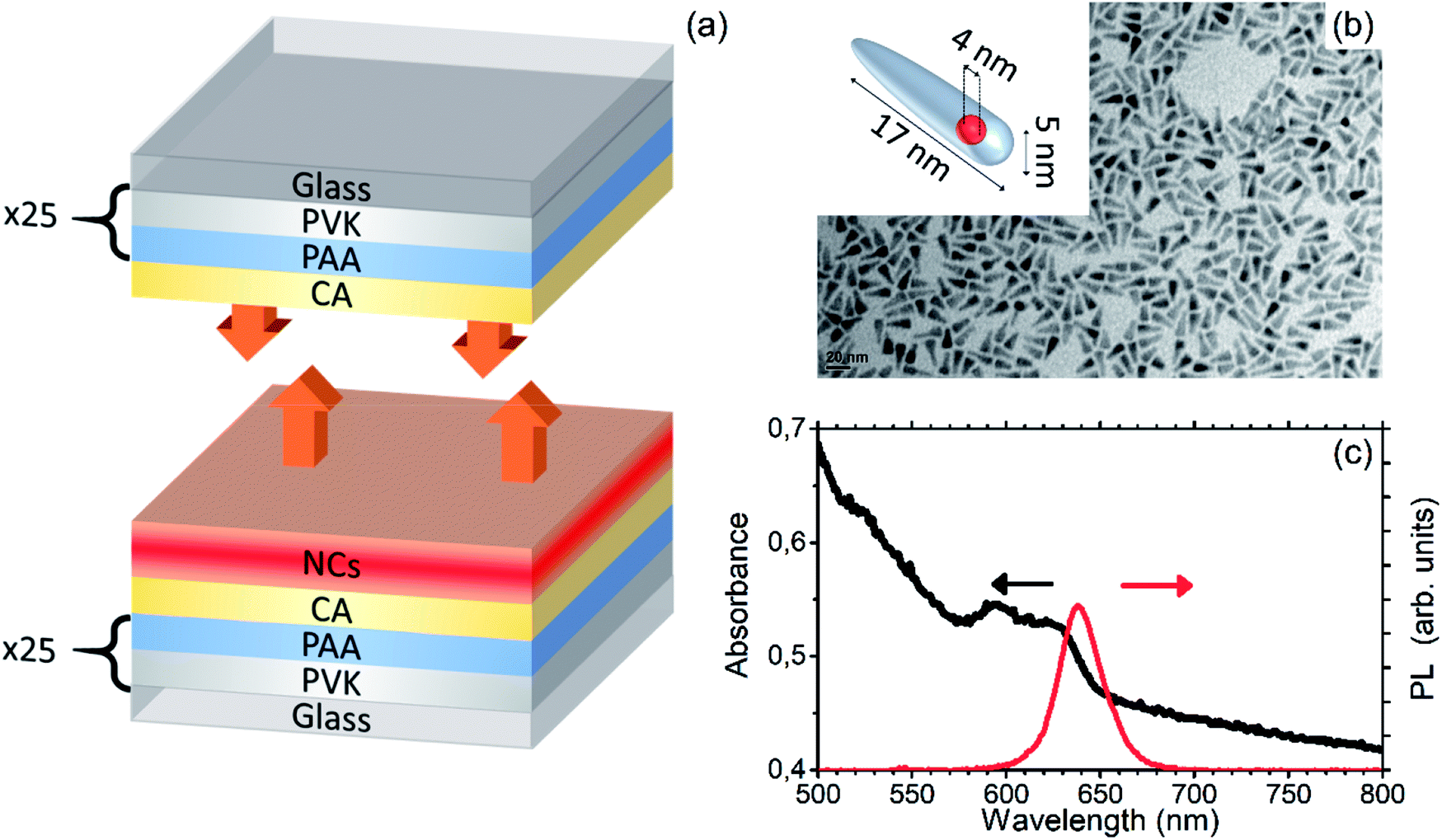 | ||
| Fig. 1 (a) Sketch of the microcavity structure, which consist of two polymer DBRs; (b) TEM image of CdSe/Cds core–shell nanocrystals; in the inset, sketch of the DiR core–shell structure; (c) absorbance (black) and CW PL (red) of the DiR film. | ||
Experimental
Colloidal nanocrystals used for this work are CdSe/CdS DiRs synthetized according to an already published procedure55 starting from CdSe cores with 4 nm diameter (see Fig. 1b). Planar microcavities have been prepared by sandwiching two identical polymer DBRs, of which one was covered by a drop-cast DiRs film. The DBRs comprise twenty-five alternated bilayers of polyacrylic acid (PAA) and polyvinylcarbazole (PVK) grown by spin-coating from solutions in 4-methyl-2-pentanol (40 g l−1, for PAA) and in toluene (40 g l−1, for PVK) at 8400 rpm on top of a 20 × 20 mm2 coverslip glass substrate. The PVK PAA polymer pair is suitable to create high quality DBRs by spin-coating as already demonstrated.56 Over each DBR, a capping layer of cellulose acetate (CA) was spun at 2400 rpm from a solution in diacetone alcohol (35 g l−1). Once completed, DBRs were annealed at 60 °C for 10 minutes. A DiRs solution in toluene (around 10 g l−1, 200 μl) was drop-cast on one DBR and the solvent was left to evaporate for 2 hours. After this step, a second DBR was pressed on top of the first one, thus creating the planar microcavity (see Fig. 1a). We also prepared a reference drop-cast DiRs film on a CA layer that had been spin-coated on a glass substrate.Angle resolved reflectance and CW photoluminescence (PL) spectra, as well as PL quantum yield (QY), have been recorded by using the optical set-up previously described,51 equipped with a high spectral resolution Ocean Optics Jazz COMBO 2 compact modular spectrometer (530–880 nm, 0.5 nm resolution).
All ASE and laser emission measurements were carried out using a Ti:sapphire laser (Coherent Legend Elite seeded by a Ti:sapphire fs laser, λ = 405 nm, 70 fs pulse FWHM and repetition rate of 1 kHz) for excitation, and an Ocean Optics HR4000 spectrometer coupled to an optical fibre for collection. The ASE measurement on the reference film was performed by focusing the excitation beam with a cylindrical lens onto the sample, thus obtaining a stripe-shaped beam profile, collecting at ∼90° with respect to the excitation beam. Laser emission measurements on the microcavities were carried out with a spherical lens at ∼0° with respect to the excitation beam, using a long-pass filter (λcut-off = 450 nm) to prevent the laser beam from reaching the detector.
TEM images were acquired using a JEOL-1100 TEM operating at an acceleration voltage of 100 kV.
Results and discussion
Fig. 1b shows a transmission electron microscopy (TEM) image of the DiRs used in this work. The DiRs have a tapered shape with average length of 17 ± 3 nm, and mean base diameter of 5 ± 1 nm (see the sketch in the inset of Fig. 1b and the size distribution histogram in ESI Fig. S1†). Fig. 1c reports the absorbance (black) and continues wave (CW) photoluminescence (PL) (red) spectra of a drop-cast DiRs film. The absorbance spectrum is characterized by a light scattering background induced by the rough film surface (ESI Fig. S2†). In spite of that, the spectrum clearly shows two peaks at about 625 and 595 nm, which are assigned to transitions related to the CdSe cores.55 The shoulder at ∼520 nm originates instead from the CdS shell. The CW PL spectrum of the DiRs film displays a single Voigt-shaped peak51 with full width half maximum (FWHM) of 27 nm, corresponding to 82 meV. The peak is centered at 639 nm and shows a 14 nm Stokes shift with respect to the band edge absorption.To investigate the ASE regime, the emission of the DiRs film was measured under fs-excitation for different pumping fluences (Fig. 2a). The presence of ASE is a necessary pre-requisite to obtain lasing from the active material in a suitable optical cavity. At fluences lower than 280 μJ cm−2, a single broad PL peak centered at 646 nm is observed. While the FWHM is unvaried, the emission peak is 6 nm red-shifted with respect to the CW measurements (see ESI Fig. S3† for a direct comparison between the two spectra). This red-shift is related to the different measurement geometry: in the CW measurements PL is collected at normal incidence, while for pulsed excitation emission it is collected at an angle of ∼90° with respect to the normal. In this condition, the longer optical path in the nanocrystal film increases self-absorption effects, and results in a spectral shift.
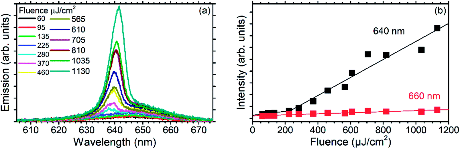 | ||
| Fig. 2 (a) DiRs film emission spectra as a function of fs-pumping fluence; (b) emission intensity at 640 (black squares) and 660 nm (red squares) as a function of excitation fluence. | ||
For fluences larger than 280 μJ cm−2, a new sharp peak is detected at 640 nm and becomes dominant with increasing excitation power density. This peak has a FWHM of 6 nm, which is ∼4 times sharper than the PL spectrum observed at low power density excitation, and appears on the high-energy side of the PL spectrum, in agreement with literature data with similar DiR emitters.57,58 Fig. 2b shows the emission intensity at 640 nm (black squares) and at 660 nm (red squares) for different pumping fluences. The intensity at 640 nm can be associated to ASE, while at 660 nm the intensity represents the overall growing trend of the PL background. At 660 nm, the PL intensity grows linearly, indicating the stability of the system under strong pumping (Fig. 2b, red line). Conversely, the intensity at 640 nm shows two different regimes: under weak pumping (below ∼280 μJ cm−2) the intensity increases linearly with a slope similar to that observed at 660 nm (Fig. 2b, black line). For higher excitation fluence, the slope dramatically increases. The comparison of the emission intensity for weak and strong excitation fluence proves that ASE occurs above a pumping threshold of ∼280 μJ cm−2, in agreement with previous observations on similar systems.36
Next, we investigate the optical properties of the polymer planar microcavity. Fig. 3a reports its reflectance spectra recorded on six different spots of the sample surface. The six spectra show minor differences, proving the homogeneity of the DBR mirrors employed to build the planar microcavity. The microcavity spectrum shows a broad and rectangular shaped reflectance peak in the spectral range 605–645 nm with FWHM of 37 nm, which is the signature of a PBG. With the refractive indexes of the two DBR media nPVK = 1.66 and nPAA = 1.51 at 640 nm,56,59–61 the measured FWHM and spectral position are compatible with those of a dielectric mirror satisfying the λ/4 condition.56,59,62,63 Although the PBG is narrower than the overall PL spectrum of the DiRs (ranging from 620 to 670 nm, see Fig. 1c), it covers the range of the ASE peak well (Fig. 2a), thus creating a functional resonator. The reflectance spectra do not show any cavity mode, which is unusual, and probably due to the reduced homogeneity in the DiRs layer as demonstrated by PL confocal maps (ESI Fig. S2†).
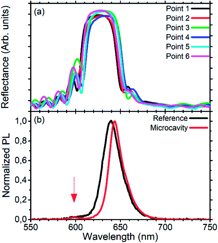 | ||
| Fig. 3 (a) Reflectance of the microcavity recorded at different spots on its surface; (b) PL spectra of the DiRs film (black line) and microcavity (red line) under CW excitation. | ||
Fig. 3b shows that the normalized PL spectra of the microcavity (red curve) and of the reference (black curve, see Experimental section for details) have minor differences under CW excitation (these spectra are reported without peak normalization in ESI Fig. S3b† for a better comparison). For the microcavity, the PL of the DiRs is suppressed in correspondence of the PBG between 600 and 640 nm, while it is nearly unchanged outside this range. This suppression due to the PBG results in a slight red-shift with respect to the reference PL. We think that the inhomogeneous thickness of the DiRs layer mentioned above hinders the detection of very sharp cavity modes (as previously observed for fully spin-coated microcavities)51 when excitation is provided over relatively large areas (∅ ∼ 1 mm) as in CW PL experiments.
The investigation of the fluorescence properties under fs-excitation for different pumping fluences shows that different spots on the microcavity surface display different behavior. Indeed, in some area only ASE was detected (see ESI Fig. S4†), while for others lasing was clearly observed. This behavior can be related to differences in the cavity length. Fig. 4a displays the emission spectra recorded for different pumping fluences in one of the resonant areas. The same spectra are also reported on a magnified scale in ESI (Fig. S5†). Fig. 4a reports the bare spectra in light colors filled to the base. These spectra show a complex structure consisting in a broad component, similar to the one observed under CW pumping, and some sharper peaks between 630 nm and 645 nm. To appreciate these features, we deconvoluted all the spectra into two components. A first broad one is obtained by multiplying the emission spectrum of the microcavity collected off-axis (black line in Fig. 4b) by a constant fitted for each emission spectrum at wavelengths larger than 645 nm. This first broad component is then subtracted from each bare spectrum to retrieve the second structured component (bold lines in Fig. 4a). The two components are indicative of two different radiative recombination pathways occurring in the microcavities. The first pathway is the PL, which is assigned to the broad component and is comparable to the bare DiR fluorescence. This PL is detected even for off-axis measurements (black line in Fig. 4b) and its intensity increases linearly with the pump fluence (red dots in Fig. 4c). The second structured component consists of several sharp peaks in the spectral range of 635 to 645 nm, which corresponds to the ASE band detected in the spectra of the reference sample (Fig. 2a and 4b). For low pumping fluences (<55 μJ cm−2), a broad signal consisting of a large number of peaks is observed. At a fluence of 55 μJ cm−2 three very sharp peaks arise at 635 nm, 637 nm, and 640 nm (ESI Fig. S5†). Upon further increasing of the pumping fluence to 110 μJ cm−2, the intensity of the peak at 640 nm grows and dominates the spectrum. The FWHM of this peak is ∼1 nm (resolution limited), which is 6-fold sharper than the ASE signal and 24-times sharper than the CW PL (Fig. 3b). These values are far above any sharpening observed for state of the art all-polymer microcavities.51 In the spectra in Fig. 4a we also notice a clear variation of the line-shape of this sharp peak with increasing pumping fluence. Such behavior cannot be explained by the spectral redistribution induced by cavity modes, which, as well-known, preserves the line-shape.20,50,51,56,64 Therefore, we conclude that the sharp peaks in the spectra originate from lasing.
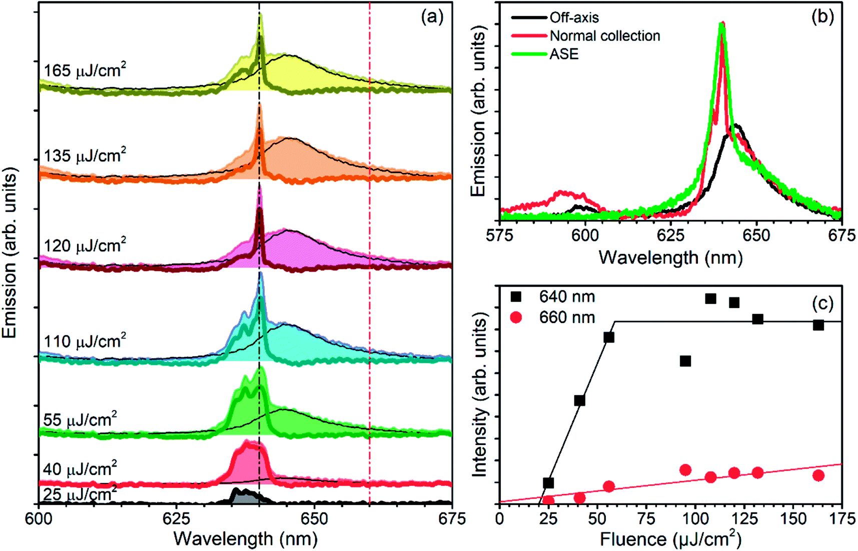 | ||
| Fig. 4 (a) Stacked fs emission spectra of the microcavity collected perpendicular (0°) to the sample surface for different pumping fluences. The original emission spectra are shown in filled light colors; the deconvoluted PL component as a black line; and the deconvoluted component with the lasing peaks as dark thick line. (b) Microcavity emission spectra under fs pumping at 110 μJ cm−2 collected at normal angle from the sample (red) and off-axis (black). Reference sample emission spectra showing ASE (in green) (c) emission intensity at 640 nm (black squares) and 660 nm (red circles) against the pump fluence. | ||
To provide further evidence of lasing emission, Fig. 4b shows emission spectra of the microcavity collected at normal incidence and slightly off-axis (collection angle < 10°) measured at a pumping fluence of 110 μJ cm−2 together with the ASE spectrum of the reference sample recorded at a pumping fluence of 460 μJ cm−2. The sharp peak at 640 nm is visible for collection under normal incidence (red line in Fig. 4b) and falls well inside the ASE emission band (green line in Fig. 4b). However, it is not detectable off-axis. This strong angular dependence is in excellent agreement with lasing from a DBR microcavity, while from spectral redistribution only a slight shift of the peak within such angles would be expected.51,64
Fig. 4c displays the intensity collected at 640 nm, assigned to the lasing mode, and at 660 nm, assigned to the PL, for increasing pumping fluence. As expected for lasing modes, the intensity of the sharp peak rises faster than the signal assigned to the PL.
To summarize, the reduced linewidth, the intensity versus pumping fluence, the spectral position, and the strong angular dependence of the sharp peaks in the microcavity spectra allows us to assign them to lasing. The evaluation of the lasing threshold from our dataset is not straightforward because we do not observe the typical kink in pump fluence-emission intensity plots. This characteristic is the direct consequence of the absence of subthreshold measures. Indeed, for the lowest fluence (25 μJ cm−2), the signal consists only in the structured component centered within in the ASE spectral range (Fig. 4a), while the intensity of the broad PL signal is below the noise level, meaning that the emissions cannot be collected at lower pumping fluences. Notwithstanding this lack, we reasonably over-estimated the lasing threshold at 50 μJ cm−2. Such threshold is in good agreement with lasing reported from similar emitting materials,36 and comparable with those observed for polymer VCSELs based on organic emitters.23,65,66 On the other hand, our upper limit for the threshold is few orders of magnitude lower than what has been reported for InGaP/ZnS core/shell NCs-polymer VCSEL fabricated by spin-coating.24 Lower thresholds have been demonstrated only for inorganic planar microcavity, where the larger dielectric contrast of the DBR media allows stronger light confinement,67–71 or more complicated resonators like microdisks.72,73
The shelf-lifetime of our samples is a parameter of great importance if we are interested in using them in real applications. To study the stability over time of the system, we measured the same lasing sample after 18 months from its production. The sample was stored in laboratory conditions without any specific care in order to test them after severe aging. As observed immediately after the production, the samples show lasing areas and non-lasing areas, being affected by the already mentioned inhomogeneity. Fig. 5a depicts the emission spectra measured for different fs pumping fluences in a spot that shows lasing. In the same plot, we also report the deconvolution of the spectra in their PL and lasing components. Similarly to the procedure used in Fig. 4a, we obtained the PL signal by multiplying the lowest power spectrum with a constant factor and fitting such value to each measured emission spectrum only for wavelengths greater than 642 nm. This component was then subtracted from the original spectrum, thus obtaining the lasing spectrum. The original spectra are shown with lightly colored filled lines, the PL components are shown as black lines, and the lasing spectra are shown with thick dark lines. Indeed, all the original emission spectra are a convolution of a broad PL signal, and by two sharp lasing peaks at 635 and 637 nm that appear for fluences larger than 2300 μJ cm−2. Fig. 5b reports the intensity of the PL and lasing components at 635 and 638 nm against pumping fluence. As expected, the PL grows linearly with fluence, while the two lasing components are negligible up to 2300 μJ cm−2 and then quickly grow linearly. Since these measures are not affected by the noise we were observing at low fluences, we are able to clearly observe the typical lasing kink with a threshold of 2300 μJ cm−2. Such value is about 50 times larger than the one measured immediately after the fabrication of the sample. Notwithstanding the low temporal stability of the lasing threshold, the directionality of the laser emission is preserved. Indeed, lasing action can be observed only within 4 degrees from the normal to the surface (ESI Fig. S6†). Already at 6°, lasing emission disappears and only a broad emission spectrum can be detected. This result further testifies that the polymer VCSEL is the source of optical feedback.
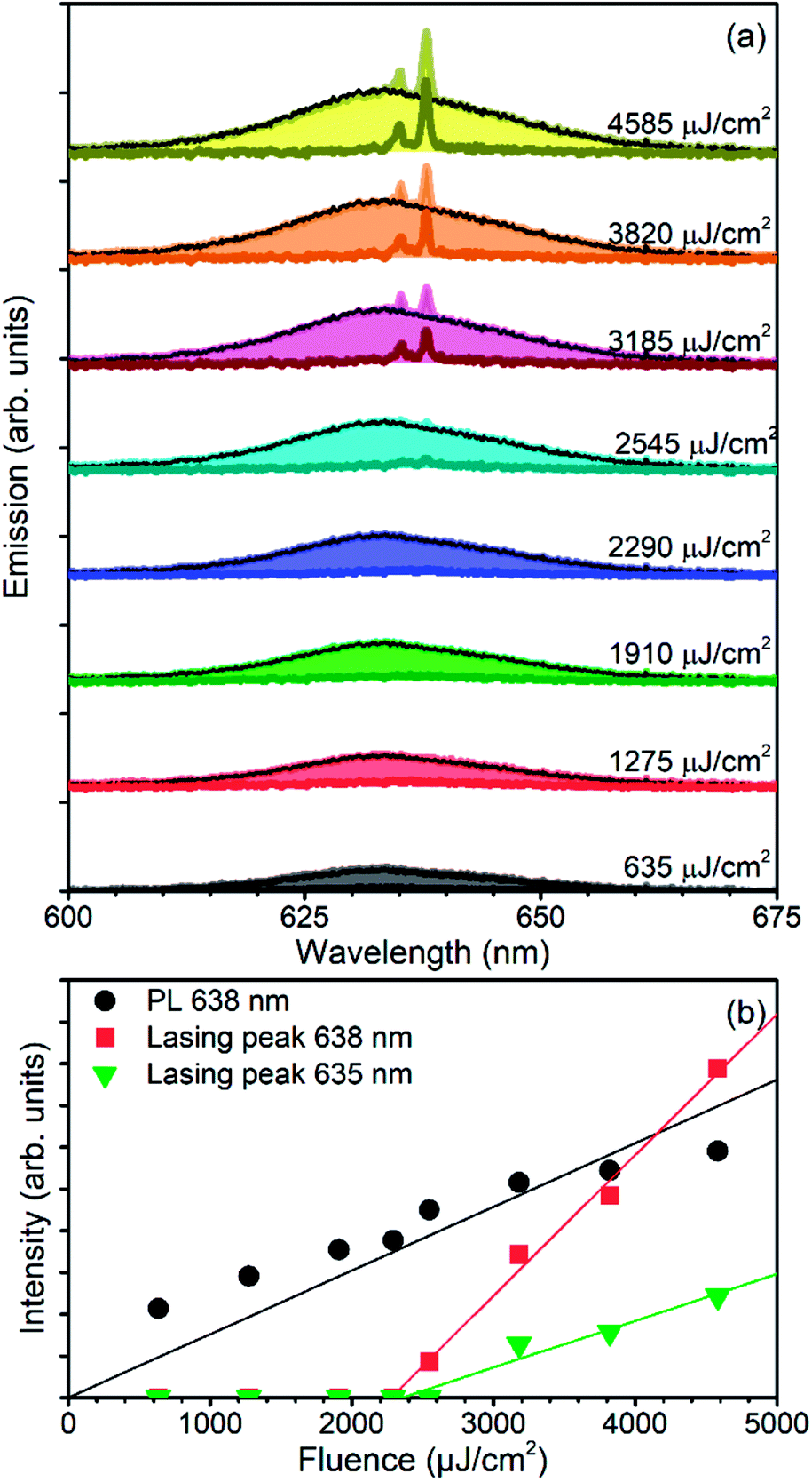 | ||
| Fig. 5 (a) Stacked fs emission spectra of the microcavity collected perpendicular (0°) to the sample surface for different pumping fluences, recorded 18 months after sample preparation. The original emission spectra are shown in filled light colors; the deconvoluted PL component as a black line; and the deconvoluted component with the lasing peaks as dark thick line. (b) Emission intensity of the PL (taken at 638 nm) and of the two lasing peaks at 635 and 638 nm as obtained by the deconvoluted spectra. | ||
Finally, lasing properties of the system degraded within 18 months agrees with the ones measured for bare DiRs used in other works57 and reveals that in order our system to be a viable option for DiRs based VCSEL, more work is needed to increase the chemical stability of DiRs, while no evident degradation occurs in the dielectric mirrors. To this end, two strategies can be envisaged. From one side, the use of novel high-density capping agents on the DiRs surface could increase their stability. Moreover, low oxygen permeability polymer matrices embedding nanocrystal, having suitable refractive index to reduce light scattering and processable growth by spin-coating for the of microcavities have to be developed to solve the problem.
Conclusions
In conclusion, we demonstrated low threshold optically pumped lasing from inorganic NCs embedded into an all-polymer VCSEL. The lasing device was manufactured by spin-coating of two PAA/PVK dielectric mirrors that embed a drop-cast layer of CdSe/CdS. The VCSEL is highly inhomogeneous but clearly shows lasing with pumping threshold of about 50 μJ cm−2, which is the lowest value reported so far for polymer-NCs systems. The system still shows lasing after 18 months from its production, but with a significantly higher threshold. Our results represent a preliminary step for the development of free-standing plastic VCSELs easily tunable over a wide spectral range and adaptable to photonic devices where low-power and simple device structures are desired.Conflicts of interest
There are no conflicts to declare.Acknowledgements
Work at UNIGE was funded by the Italian Ministry of University, Research and Instruction through the “Progetti di Ricerca di Rilevante Interesse Nazionale 2010–2011” Program (Materiali Polimerici Nanostrutturati con strutture molecolari e cristalline mirate, per tecnologie avanzate e per l'ambiente, 2010XLLNM3). P. L. is thankful for support by the European Union's Horizon 2020 research and innovation program under the Marie Sklodowska-Curie Grant Agreement No. 643238.Notes and references
- Z. Tan, C. Yang, Y. Zhu, Z. Xu, K. Zou, F. Zhang and Z. Wang, IEEE Photonics Technol. Lett., 2017, 29, 751–754 CrossRef.
- N. Sheffi and D. Sadot, J. Lightwave Technol., 2017, 35, 2098–2108 CrossRef CAS.
- S. K. Pavan, J. Lavrencik and S. E. Ralph, J. Lightwave Technol., 2017, 35, 1614–1623 CrossRef CAS.
- S. Haruhisa, I. Ken-ichi, K. Chiyuki and S. Yasuharu, Jpn. J. Appl. Phys., 1979, 18, 2329 CrossRef.
- F. Koyama, J. Lightwave Technol., 2006, 24, 4502–4513 CrossRef CAS.
- A. C. Scofield, S.-H. Kim, J. N. Shapiro, A. Lin, B. Liang, A. Scherer and D. L. Huffaker, Nano Lett., 2011, 11, 5387–5390 CrossRef CAS PubMed.
- B. Hu, G. Jin, T. Liu and J. Wang, Photonic Sens., 2016, 6, 351–358 CrossRef.
- C. J. Chang-Hasnain, IEEE J. Sel. Top. Quantum Electron., 2000, 6, 978–987 CrossRef CAS.
- K. J. Vahala, Nature, 2003, 424, 839–846 CrossRef CAS PubMed.
- T. Mizunami, T. Yamada and S. Tsuchiya, Opt. Rev., 2016, 23, 703–707 CrossRef.
- K. Iga, IEEE J. Sel. Top. Quantum Electron., 2000, 6, 1201–1215 CrossRef CAS.
- S. Jatta, K. Zogal, B. Kögel, K. Haberle, C. Sydlo and P. Meissner, Frequenz, 2008, 62, 96–99 CrossRef.
- W. G. Breiland, A. A. Allerman, J. F. Klem and K. E. Waldrip, MRS Bull., 2011, 27, 520–524 CrossRef.
- J. H. Andrews, M. Crescimanno, N. J. Dawson, G. Mao, J. B. Petrus, K. D. Singer, E. Baer and H. Song, Opt. Express, 2012, 20, 15580–15588 CrossRef CAS PubMed.
- H. Song, K. Singer, J. Lott, Y. Wu, J. Zhou, J. Andrews, E. Baer, A. Hiltner and C. Weder, J. Mater. Chem., 2009, 19, 7520–7524 RSC.
- Q. H. L. Hou, Y. Mo, J. Peng and Y. Cao, Appl. Phys. Lett., 2005, 87, 243504 CrossRef.
- M. F. Weber, C. A. Stover, L. R. Gilbert, T. J. Nevitt and A. J. Ouderkirk, Science, 2000, 287, 2451 CrossRef CAS PubMed.
- J.-H. Lee, C. Y. Koh, J. P. Singer, S.-J. Jeon, M. Maldovan, O. Stein and E. L. Thomas, Adv. Mater., 2014, 26, 532–569 CrossRef CAS PubMed.
- D. Comoretto, Organic and Hybrid Photonic Crystals, Springer International Publishing, Switzerland, 2015 Search PubMed.
- S. Gazzo, G. Manfredi, R. Pötzsch, Q. Wei, M. Alloisio, B. Voit and D. Comoretto, J. Polym. Sci., Part B: Polym. Phys., 2016, 54, 73–80 CrossRef CAS.
- P. Lova, C. Bastianini, P. Giusto, M. Patrini, P. Rizzo, G. Guerra, M. Iodice, C. Soci and D. Comoretto, ACS Appl. Mater. Interfaces, 2016, 8, 31941–31950 CAS.
- P. Lova, D. Cortecchia, H. N. S. Krishnamoorthy, P. Giusto, C. Bastianini, A. Bruno, D. Comoretto and C. Soci, ACS Photonics, 2018, 5, 867–874 CrossRef CAS.
- G. Canazza, F. Scotognella, G. Lanzani, S. D. Silvestri, M. Zavelani-Rossi and D. Comoretto, Laser Phys. Lett., 2014, 11, 035804 CrossRef.
- V. M. Menon, M. Luberto, N. V. Valappil and S. Chatterjee, Opt. Express, 2008, 16, 19535–19540 CrossRef CAS PubMed.
- T. Komikado, S. Yoshida and S. Umegaki, Appl. Phys. Lett., 2006, 89, 061123 CrossRef.
- F. Scotognella, A. Monguzzi, M. Cucini, F. Meinardi, D. Comoretto and R. Tubino, Int. J. Photoenergy, 2008, 2008, 4 CrossRef.
- C. Burda, X. Chen, R. Narayanan and M. A. El-Sayed, Chem. Rev., 2005, 105, 1025–1102 CrossRef CAS PubMed.
- A. P. Alivisatos, Science, 1996, 271, 933 CAS.
- Q. Sun, Y. A. Wang, L. S. Li, D. Wang, T. Zhu, J. Xu, C. Yang and Y. Li, Nat. Photonics, 2007, 1, 717–722 CrossRef CAS.
- J. Q. Grim, L. Manna and I. Moreels, Chem. Soc. Rev., 2015, 44, 5897–5914 RSC.
- I. Angeloni, W. Raja, R. Brescia, A. Polovitsyn, F. De Donato, M. Canepa, G. Bertoni, R. Proietti Zaccaria and I. Moreels, ACS Photonics, 2016, 3, 58–67 CrossRef CAS.
- http://www.nanosysinc.com/, (accessed 03/22/2018).
- J. Q. Grim, S. Christodoulou, F. Di Stasio, R. Krahne, R. Cingolani, L. Manna and I. Moreels, Nat. Nanotechnol., 2014, 9, 891–895 CrossRef CAS PubMed.
- C. B. Murray, D. J. Norris and M. G. Bawendi, J. Am. Chem. Soc., 1993, 115, 8706–8715 CrossRef CAS.
- X. Peng, L. Manna, W. Yang, J. Wickham, E. Scher, A. Kadavanich and A. P. Alivisatos, Nature, 2000, 404, 59–61 CrossRef CAS PubMed.
- F. Di Stasio, J. Q. Grim, V. Lesnyak, P. Rastogi, L. Manna, I. Moreels and R. Krahne, Small, 2015, 11, 1328–1334 CrossRef CAS PubMed.
- I. Moreels, G. Rainò, R. Gomes, Z. Hens, T. Stöferle and R. F. Mahrt, Adv. Mater., 2012, 24, OP231–OP235 CrossRef CAS PubMed.
- L. Qu and X. Peng, J. Am. Chem. Soc., 2002, 124, 2049–2055 CrossRef CAS PubMed.
- B. S. Mashford, M. Stevenson, Z. Popovic, C. Hamilton, Z. Zhou, C. Breen, J. Steckel, V. Bulovic, M. Bawendi, S. Coe-Sullivan and P. T. Kazlas, Nat. Photonics, 2013, 7, 407–412 CrossRef CAS.
- F. Di Stasio, A. Polovitsyn, I. Angeloni, I. Moreels and R. Krahne, ACS Photonics, 2016, 3, 2083–2088 CrossRef CAS.
- C. Dang, J. Lee, C. Breen, J. S. Steckel, S. Coe-Sullivan and A. Nurmikko, Nat. Nanotechnol., 2012, 7, 335–339 CrossRef CAS PubMed.
- Y.-S. Park, W. K. Bae, T. Baker, J. Lim and V. I. Klimov, Nano Lett., 2015, 15, 7319–7328 CrossRef CAS PubMed.
- V. I. Klimov, S. A. Ivanov, J. Nanda, M. Achermann, I. Bezel, J. A. McGuire and A. Piryatinski, Nature, 2007, 447, 441–446 CrossRef CAS PubMed.
- Y. Kelestemur, A. F. Cihan, B. Guzelturk and H. V. Demir, Nanoscale, 2014, 6, 8509–8514 RSC.
- C. Grivas, C. Li, P. Andreakou, P. Wang, M. Ding, G. Brambilla, L. Manna and P. Lagoudakis, Nat. Commun., 2013, 4, 2376 Search PubMed.
- F. Fan, O. Voznyy, R. P. Sabatini, K. T. Bicanic, M. M. Adachi, J. R. McBride, K. R. Reid, Y.-S. Park, X. Li, A. Jain, R. Quintero-Bermudez, M. Saravanapavanantham, M. Liu, M. Korkusinski, P. Hawrylak, V. I. Klimov, S. J. Rosenthal, S. Hoogland and E. H. Sargent, Nature, 2017, 544, 75–79 CrossRef CAS PubMed.
- M. M. Adachi, F. Fan, D. P. Sellan, S. Hoogland, O. Voznyy, A. J. Houtepen, K. D. Parrish, P. Kanjanaboos, J. A. Malen and E. H. Sargent, Nat. Commun., 2015, 6, 8694 CrossRef CAS PubMed.
- R. R. K. Unger, C. Czibula, C. Ganser, C. Teichert, G. Jakopic, G. Canazza, S. Gazzo and D. Comoretto, Distributed Bragg reflectors: morphology of cellulose acetate and polystyrene multilayers, Graz, Austria, 2014 Search PubMed.
- G. Manfredi, C. Mayrhofer, G. Kothleitner, R. Schennach and D. Comoretto, Cellulose, 2016, 23, 2853–2862 CrossRef CAS.
- R. J. Knarr III, G. Manfredi, E. Martinelli, M. Pannocchia, D. Repetto, C. Mennucci, I. Solano, M. Canepa, F. Buatier de Mongeot, G. Galli and D. Comoretto, Polymer, 2016, 84, 383–390 CrossRef.
- G. Manfredi, P. Lova, F. Di Stasio, R. Krahne and D. Comoretto, ACS Photonics, 2017, 4, 1761–1769 CrossRef CAS.
- P. Lova, G. Manfredi, L. Boarino, A. Comite, M. Laus, M. Patrini, F. Marabelli, C. Soci and D. Comoretto, ACS Photonics, 2015, 2, 537–543 CrossRef CAS.
- P. Lova, G. Manfredi, L. Boarino, M. Laus, G. Urbinati, T. Losco, F. Marabelli, V. Caratto, M. Ferretti, M. Castellano, C. Soci and D. Comoretto, Phys. Status Solidi C, 2015, 12, 158–162 CrossRef CAS.
- F. D. Stasio, L. Berti, M. Burger, F. Marabelli, S. Gardin, T. Dainese, R. Signorini, R. Bozio and D. Comoretto, Phys. Chem. Chem. Phys., 2009, 11, 11515–11519 RSC.
- L. Carbone, C. Nobile, M. De Giorgi, F. D. Sala, G. Morello, P. Pompa, M. Hytch, E. Snoeck, A. Fiore, I. R. Franchini, M. Nadasan, A. F. Silvestre, L. Chiodo, S. Kudera, R. Cingolani, R. Krahne and L. Manna, Nano Lett., 2007, 7, 2942–2950 CrossRef CAS PubMed.
- P. Lova, V. Grande, G. Manfredi, M. Patrini, S. Herbst, F. Würthner and D. Comoretto, Adv. Opt. Mater., 2017, 5, 1700523 CrossRef.
- M. Z. Rossi, R. Krahne, G. D. Valle, S. Longhi, I. R. Franchini, S. Girardo, F. Scotognella, D. Pisignano, L. Manna, G. Lanzani and F. Tassone, Laser Photonics Rev., 2012, 6, 678–683 CrossRef.
- H. Zhao, G. Sirigu, A. Parisini, A. Camellini, G. Nicotra, F. Rosei, V. Morandi, M. Zavelani-Rossi and A. Vomiero, Nanoscale, 2016, 8, 4217–4226 RSC.
- L. Fornasari, F. Floris, M. Patrini, D. Comoretto and F. Marabelli, Phys. Chem. Chem. Phys., 2016, 18, 14086–14093 RSC.
- D. Comoretto, G. Dellepiane, C. Cuniberti, L. Rossi, A. Borghesi and J. Le Moigne, Phys. Rev. B: Condens. Matter Mater. Phys., 1996, 53, 15653–15659 CrossRef CAS.
- G. Lanzani, M. Zavelani-Rossi, G. Cerullo, D. Comoretto and G. Dellepiane, Phys. Rev. B: Condens. Matter Mater. Phys., 2004, 69, 134302 CrossRef.
- J. D. Joannopulos, R. D. Meade and J. N. Win, Photonic Crystals: Molding the Flow of the Light, Princeton University Press, Princeton, 1995 Search PubMed.
- M. Skorobogatiy and J. Yang, Fundamentals of Photonic Crystal Guiding, 2009, pp. 1–267 Search PubMed.
- L. Frezza, M. Patrini, M. Liscidini and D. Comoretto, J. Phys. Chem. C, 2011, 115, 19939–19946 CAS.
- H. Takeuchi, K. Natsume, S. Suzuki and H. Sakata, Electron. Lett., 2007, 43, 30–32 CrossRef CAS.
- L. M. Goldenberg, V. Lisinetskii, Y. Gritsai, J. Stumpe and S. Schrader, Opt. Mater. Express, 2012, 2, 11–19 CrossRef CAS.
- A. Palatnik, H. Aviv and Y. R. Tischler, ACS Nano, 2017, 11, 4514–4520 CrossRef CAS PubMed.
- Y. Ding, H. Fan, X. Zhang, X. Jiang and M. Xiao, Opt. Commun., 2017, 395, 51–54 CrossRef CAS.
- T.-W. Lee, O. O. Park, H. N. Cho, D. Y. Kim and Y. C. Kim, J. Appl. Phys., 2003, 93, 1367–1370 CrossRef CAS.
- A. Palatnik and Y. R. Tischler, IEEE Photonics Technol. Lett., 2016, 28, 1823–1826 CrossRef CAS.
- L. Persano, A. Camposeo, P. D. Carro, E. Mele, R. Cingolani and D. Pisignano, Appl. Phys. Lett., 2006, 89, 121111 CrossRef.
- H. Sun, X. Chen, H. Wang, Q. Lu, H. Yang, S. Xie and X. Wu, IEEE Photonics J., 2017, 9, 1–6 Search PubMed.
- H. Yoshioka, T. Ota, C. Chen, S. Ryu, K. Yasui and Y. Oki, Sci. Rep., 2015, 5, 10623 CrossRef PubMed.
Footnotes |
| † Electronic supplementary information (ESI) available: DiRs size distribution. DiRs film confocal microscopy. Spectral comparison of the DiRs PL. Fluence dependence of emission in regions that do not show lasing. Rescaled lasing spectra and cavity thickness estimation. Lasing from the microcavity and deconvolution. See DOI: 10.1039/c8ra01282b |
| ‡ Present address: Center for Nano Science and Technology, Istituto Italiano di Tecnologia, Milano, Italy. |
| § Present address: ICFO – The Institute of Photonic Sciences, Castelldefels (Barcelona), Spain. |
| This journal is © The Royal Society of Chemistry 2018 |