
 Open Access Article
 This Open Access Article is licensed under a Creative Commons Attribution-Non Commercial 3.0 Unported Licence
Resistive non-volatile memories fabricated with poly(vinylidene fluoride)/poly(thiophene) blend nanosheets†
Huie Zhu *a,
Shunsuke Yamamotoa,
Jun Matsuib,
Tokuji Miyashitaa and
Masaya Mitsuishi*a
*a,
Shunsuke Yamamotoa,
Jun Matsuib,
Tokuji Miyashitaa and
Masaya Mitsuishi*a
aInstitute of Multidisciplinary Research for Advanced Materials (IMRAM), Tohoku University, 2-1-1 Katahira, Aoba-ku, Sendai 980-8577, Japan. E-mail: zhuhuie@tohoku.ac.jp; masaya@tohoku.ac.jp
bDepartment of Material and Biological Chemistry, Faculty of Science, Yamagata University, 1-4-12 Kojirakawamachi, Yamagata 990-8560, Japan
First published on 20th February 2018
Abstract
Ferroelectric poly(vinylidene fluoride)/semiconductive polythiophene (P3CPenT) blend monolayers were developed at varying blend ratios using the Langmuir–Blodgett technique. The multilayered blend nanosheets show much improved surface roughness that is more applicable for electronics applications than spin-cast films. Because of the precisely controllable bottom-up construction, semiconductive P3CPenT were well dispersed into the ferroelectric PVDF matrix. Moreover, the ferroelectric matrix contains almost 100% β crystals: a polar crystal phase responsible for the ferroelectricity of PVDF. Both the good dispersion of semiconductive P3CPenT and the outstanding ferroelectricity of the PVDF matrix in the blend nanosheets guaranteed the success of ferroelectric organic non-volatile memories based on ferroelectricity-manipulated resistive switching with a fresh high ON/OFF ratio and long endurance to 30 days.
Ferroelectric capacitors memorize information by the two antiparallel polarization states coded as “0” or “1”, even after removing the applied power, serving as non-volatile memory.1,2 However, the reading out of the stored information in such memories will change the polarization state, which is known as destructive read-out. To realize non-destructive read-out and low-energy writing in such devices, conjugated polymers were introduced into a ferroelectric polymer matrix to form phase-separated blends, which contributed to novel ferroelectric resistive switches with very simple two-terminal sandwiched devices superior to the complicated transistor type electronic elements.3,4 In the ferroelectric nonvolatile memories, the bi-stable polarization states in ferroelectric polymers such as poly(vinylidene fluoride) (PVDF) derivatives were used to manipulate the charge transfer and injection in conjugated polymers (CPs).3–7 This manipulation results in different resistance at on-state and off-state of the devices controlled by the ferroelectric polarization directions. Consequently, non-destructive low-voltage operation was realized in which the ferroelectric PVDF provides switching functionality. The read-out operation is performed by conduction through a nearby semiconducting layer.5 Thereafter, the operational mechanism of ferroelectric-driven organic resistive switches was clarified by Kemerink et al.8 They stressed that the stray field of the polarized ferroelectric phase can modulate the charge injection from a metallic electrode into the organic semiconductor, switching the diode from injection-limited to space-charge-limited.
Although the devices show promising applications, the random phase-separation morphology gives them uncertain properties.9,10 The most important obstacle is to prepare well-dispersive PVDF–CP phase-separated blend nanofilms because a well-dispersive hybrid nanofilm is indispensable for higher information storage density. In other words, embedding semiconductor polymers into ferroelectric polymer matrixes with domain size of CPs smaller than a few tens of nanometers (e.g. 50 nm) has remained extremely challenging to date.6,9 Phase-separated films prepared using traditional methods such as spin-coating show a much disordered surface with root-mean-square (RMS) roughness exceeding 39.97 nm.11 Such a highly rough surface tends to induce large leakage current. Especially, the annealing treatment for PVDF materials to increase crystallinity and ferroelectric phase crystals also brings a significant increment to the phase-separated domain size. From another perspective, to decrease the writing and read-out operational voltages, ultrathin blend films (thinner than 100 nm) with high-content ferroelectric crystals are also necessary. However, the reported methods to prepare polymer ferroelectric ultrathin films, e.g. spin-coating are usually performed at the cost of decreasing the ferroelectric phase or requiring high energy consumption.
Previous reports have proposed a versatile method to achieve highly oriented ferroelectric polymer Langmuir–Blodgett (LB) nanofilms consisting of ferroelectric poly(vinylidene fluoride) (PVDF) and tiny amphiphilic poly(N-dodecylacrylamide) (pDDA) supplying film stability at the air–water interface and transfer properties (Fig. 1a).12,13 The LB nanofilms, with a controllable film thickness at several nanometers' scale and a smooth film surface, can be transferred onto solid and flexible substrates irrespective of their surface wettability. The contents of ferroelectric β crystals in the as-prepared nanofilms with no post-treatment can be up to 95%, which is the best content in such thin films ever reported.2,14 Therefore, we investigated a strongly enhanced ferroelectricity of the PVDF LB nanofilms with no electrical poling showing one of the highest ferroelectric remanent polarization values, 6.6 μC cm−2, for nanometer-scale films, in addition to long endurance because of the high orientation of β crystals.2 The PVDF–pDDA LB nanofilms benefit both from the good film-formation properties of amphiphilic pDDA and the functionality of ferroelectric PVDF. To extend their applications, the PVDF–pDDA LB nanofilms are promising for application as a platform and matrix to combine with other functional materials such as organic functional materials and inorganic nanoparticles. Similarly, it is promising for production of well-dispersive ferroelectric/semiconductive polymer blends by addition of a third composition: semiconductive polymers at the air–water interface. Moreover, we have reported that semiconductive poly(3-hexylthiophene) (P3HT) monolayers were stabilized by mixing with the amphiphilic poly(N-dodecylacrylamide) (pDDA) at the air–water interface for field-effect transistors.15
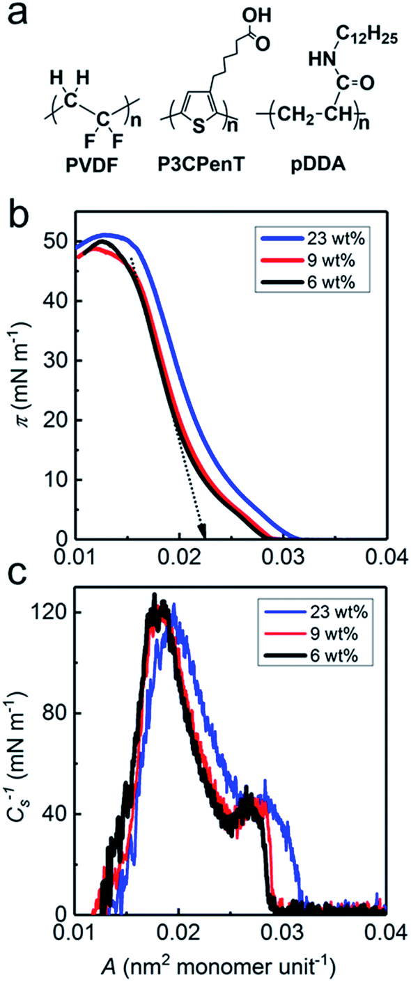 | ||
| Fig. 1 (a) Chemical structures of poly(vinylidene fluoride) (PVDF), poly[3-(5-carboxypentyl) thiophene-2,5-diyl] (P3CPenT) and poly(N-dodecylacrylamide) (pDDA), (b) surface pressure (π)–area (A) isotherms, and (c) compressibility modulus (Cs−1)–surface area (A) isotherms of PVDF–P3CPenT–pDDA Langmuir films for various weight contents of P3CPenT relative to PVDF. The straight arrow in (b) indicates the line extrapolated to determine the limiting surface area. | ||
This study examines the facile preparation of blend nanosheets of ferroelectric PVDF and semiconductive polymer, by incorporating poly[3-(5-carboxypentyl) thiophene-2,5-diyl] (P3CPenT) into PVDF–pDDA Langmuir–Blodgett (LB) nanofilms. P3CPenT is a conjugated polythiophene carboxylate (Fig. 1a) that occupies superior charge transport performance resulting from a delicate balance between its solubility and solid-state film morphologies.16,17 The blend LB nanosheets can be transferred readily and regularly from the air–water interface onto various substrates. Phase-separation morphologies were studied based on the varying P3CPenT contents. Resistive switching properties were demonstrated in a simple sandwiched device of Al/PVDF–P3CPenT–pDDA/Au at the opposite polarization direction of the PVDF matrix.
The PVDF–P3CPenT–pDDA monolayers were prepared by spreading PVDF–P3CPenT mix solution and pDDA solution onto water surface in sequence at a molar ratio of 50![[thin space (1/6-em)]](https://www.rsc.org/images/entities/char_2009.gif) :1 (see ESI† for details). Fig. 1b shows surface pressure (π)–area (A) isotherms of PVDF–P3CPenT–pDDA Langmuir films at varying P3CPenT contents (relative to PVDF) at 20 °C: they are designated as P3CPenT 6 wt%, P3CPenT 9 wt% and P3CPenT 23 wt%. The sharply rising curves with high collapse surface pressures up to 50 mN m−1 are indicative of the formation of stable and compact Langmuir blend monolayers at the air–water interface. These pressure values are much higher than those of pure PVDF (25 mN m−1) or P3CPenT (15 mN m−1) (Fig. S1†). Results suggest that amphiphilic pDDA can greatly improve film stability at the air–water interface because of excellent hydrogen bonding interactions that occur among the amide groups in pDDA backbones.13 The compressibility modulus (or elasticity) Cs−1 was calculated from isotherm data based on eqn (1) to obtain the monolayer elastic behavior.18
:1 (see ESI† for details). Fig. 1b shows surface pressure (π)–area (A) isotherms of PVDF–P3CPenT–pDDA Langmuir films at varying P3CPenT contents (relative to PVDF) at 20 °C: they are designated as P3CPenT 6 wt%, P3CPenT 9 wt% and P3CPenT 23 wt%. The sharply rising curves with high collapse surface pressures up to 50 mN m−1 are indicative of the formation of stable and compact Langmuir blend monolayers at the air–water interface. These pressure values are much higher than those of pure PVDF (25 mN m−1) or P3CPenT (15 mN m−1) (Fig. S1†). Results suggest that amphiphilic pDDA can greatly improve film stability at the air–water interface because of excellent hydrogen bonding interactions that occur among the amide groups in pDDA backbones.13 The compressibility modulus (or elasticity) Cs−1 was calculated from isotherm data based on eqn (1) to obtain the monolayer elastic behavior.18
| Cs−1 = −A(dπ/dA) | (1) |
In the Cs−1–A curves shown in Fig. 1c, each compressed Langmuir film shows a peak value of Cs−1*, manifesting the formation of a critical concentrated solid state.19–22 Table S1† shows the limiting surface area (Saver), collapse surface pressure (πc), peak compressibility modulus (Cs−1*), corresponding surface pressure (π*), and corresponding occupied area (A*) for the respective P3CPenT contents. The change in the limiting surface area from 0.0224 (6 wt%) to 0.0250 nm2 (23 wt%) shows the successful introduction of P3CPenT into the PVDF matrix.
After confirming the film formation properties, the monolayers were transferred onto hydrophobic silicon substrates regularly (Fig. S2†). The transfer ratios for both downstrokes and upstrokes are almost unity, based on eqn (S1).† Low surface roughness is a crucially important parameter for electronic applications. In earlier reports, lowering the root-mean-square (RMS) roughness below 30 nm is quite a challenge for the ferroelectric/semiconductive polymer blend films because of the crystalline properties of the two polymers. The AFM images (Fig. 2a–d) of the as-prepared PVDF–P3CPenT blend LB nanosheets manifest much smoother surfaces, even for the 80-layer nanosheets by an RMS value of 10.8 nm. This value is smaller than that of the reported spin-coating films.6,11 In Fig. 2c, the nanofiber structures in the P3CPenT 23 wt% monolayer orientate at one direction as the black arrow indicates. All the nanofibers show a regular size of 7.9 nm (Fig. 2e). In contrast, such nanofiber structures do not appear in the monolayers at low contents of P3CPenT in Fig. 2a and b, which proves that the nanofiber structures originate from P3CPenT molecules. In Fig. 2d and S3,† the interlaced nanofiber networks in the 80-layer LB blend nanosheet caused by repeated deposition of Langmuir monolayers will provide the nodal points for electric conductivity. EDX mapping images show homogeneous dispersion of P3CPenT in PVDF, which also ensured the continuous conducting path (Fig. S4†), while the nano-domains were not clear seen. It may originate from the similar solubility of PVDF and P3CPenT in NMP, which made the unclear phase-separation structure.
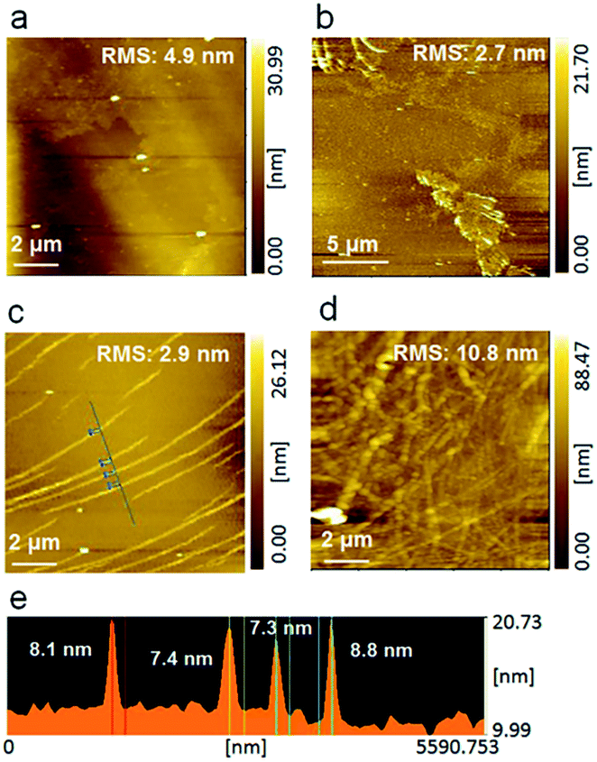 | ||
| Fig. 2 AFM images of (a)–(c) PVDF–P3CPenT–pDDA blend LB monolayer at 6, 9, and 23 wt% P3CPenT, (d) an 80-layer blend LB nanosheet (P3CPenT 23 wt%), and (e) height profile of the fiber structures in (c). | ||
The blend monolayers were readily transferred onto various substrates such as rigid silicon and flexible PET substrates (Fig. 3). The uniform interference colours of the macroscopic films at each layer number are indicative of the regular layer structures and homogeneous film transfer from water surface to the substrates. The result also evidenced the controllable preparation of functional polymer blends at several nanometres' scale for the present work, which cannot be achieved by general film preparation methods such as drop casting and spin-coating. UV-vis spectra in Fig. 4a show a broad absorbance peak near 462 nm for P3CPenT and PVDF–P3CPenT solutions in NMP. The detected absorbance peaks at 442, 428, and 415 nm at 23 wt%, 9 wt%, and 6 wt%, respectively, evidenced the successful introduction of P3CPenT into the PVDF LB nanofilms (Fig. 4b). The tunable domain size and controllable film thickness are not the only virtues of the blend nanosheets. In Fig. 5a, the FT-IR spectra of the blend nanosheets show significant peaks at 508, 840, 1276, and 1400 cm−1 at each content, which are assigned for the ferroelectric β crystals (Form I).23–25 Characteristic peaks of paraelectric α crystals (763 and 976 cm−1) were not detected. The rich β phase formation was also confirmed using XRD patterns, which showed the appearance of 110/200 reflection at 20.1° (Fig. S5†).12,25 The PVDF–pDDA LB films were crystalline films with a crystallinity of 50%.12 Results confirmed that the blend nanosheets contain almost 100% ferroelectric β crystal, which is consistent with the reported value for PVDF–pDDA LB nanofilms,12 indicating that the addition of P3CPenT did not affect the crystal structures of PVDF. The result ensures that the ferroelectric matrix in the blend nanosheets can supply a stable and large polarization electric field to modulate charge transfer and accumulation. Monolayer thickness was confirmed as 2.3, 2.6, and 2.6 nm respective for 6 wt%, 9 wt%, and 23 wt% P3CPenT containing LB nanosheets by XRD spectra (Fig. S6 and Table S2†). All the monolayers can be uniformly and repeatedly transferred to substrates to adjust the film thickness. Therefore, the film thickness of the nanosheets can be finely modulated at several nanometres' scale.2 This report is the first of the relevant literature to describe success on the preparation of blend LB nanosheets with highly ferroelectric matrix and well-dispersive semiconductive P3CPenT.
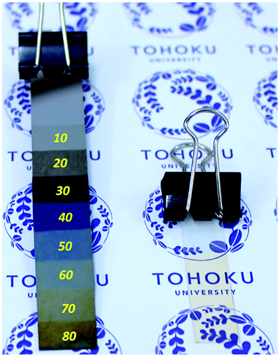 | ||
| Fig. 3 Photographs of blend LB nanosheets with 23 wt% P3CPenT at various layers on Si substrate (left) and a 30-layer blend nanosheet on flexible PET membrane (right). | ||
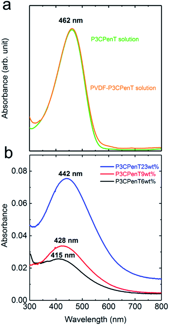 | ||
| Fig. 4 UV-vis absorption spectra of (a) P3CPenT and PVDF–P3CPenT solutions in NMP and (b) the blend LB nanosheets for various weight contents of P3CPenT relative to PVDF. | ||
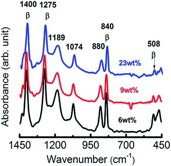 | ||
| Fig. 5 FT-IR spectra of 80-layer PVDF–P3CPenT–pDDA blend nanosheets for various P3CPenT contents. | ||
Memory devices were constructed with a simple sandwiched structure: glass substrate/gold (Au)/blend LB nanofilms/aluminum (Al) (see the inset of Fig. S7 and ESI†).26,27 Fig. S7a† shows typical current (I)–voltage (V) characteristics of 30-layer blend nanosheets (78 nm), which demonstrated a reversal current hysteresis with voltage sweeping between ±20 V.9,11 The cross-sectional SEM image of the memory device is shown in Fig. S7b,† indicating a well-defined layer structure. The current can only flow through the P3CPenT domains because of the insulation characteristic of PVDF matrix, however, no hysteresis loop was obtained for the blend LB nanosheets. This is due to the conducting path formed by the interlaced P3CPenT nanofibers even with the presence of rich ferroelectric β phase. So our device will not follow Asadi's mechanism as introduced in the Introduction part.
Local surface potential patterns were visualized using Kelvin probe microscopy to investigate the polarization state of the devices.12 A two-step measurement was conducted (Fig. 6a). First, a positive/negative bias voltage was applied to the conductive AFM cantilever under ambient conditions, making the sample surface polarized with a square shape. Then, the KFM mode was conducted to obtain images of the polarized patterns, which is called the reading procedure. Fig. 6b and c portray the surface potential images before and after polarization. Clearly, the inverse profile of the positive and negative polarized area is seen in Fig. 6b, which indicates the LB films are ferroelectric.
 | ||
| Fig. 6 (a) Schematic illustration of Kelvin probe force microscopy measurement and surface potential images (b) before polarization and (c) after polarization. | ||
To investigate whether the device is resistive switching or not, we applied a polarizing pulse for information writing with pulse width of 2.5 s and voltage of 30 V to induce polarization states of the ferroelectric matrix in a 40-layer blend nanosheet (104 nm) as shown in Fig. 7a. The pristine state refers to as-fabricated devices that have not undergone any electrical poling. The writing voltage magnitude for both ON and OFF states is set as 30 V for 2.5 s higher than its coercive voltage: 20 V (195 MV m−1 × 10⁴ nm)2 of the PVDF LB nanosheet, as we previously reported, to ensure the high polarization value in the ferroelectric matrix. The read-out operation was operated at quite low voltage by detecting the current flow in the devices. The blend nanosheet after polarizing at +30 V exerts ten-fold improved current density (ON-state) in comparison with the pristine nanosheet before polarization (Fig. 7b). In contrast, the current density decreased after polarization at −30 V (OFF-state). The results verified the resistive switching characteristics and the non-volatility nature of the memory devices fabricated with the blend nanosheets. For comparison, a control experiment for pure pDDA LB nanofilms showed no ferroelectric polarization-reversal-induced resistive switching (Fig. S8†). It is noteworthy that by combining the ferroelectric PVDF nanosheet with semiconductive polymer, the read-out voltage is optimized even to lower than 1 V. Results show that it is highly competitive over the ferroelectric capacitors without semiconductive components, which require a reading-out voltage higher than coercive voltage, about 20 V for the 100 nm-thick films.2 The ON/OFF ratio values were recorded at varying reading voltages (Fig. 7c). The maximum value of the ON/OFF ratio was approximately 891 with increasing read-out voltage to 15 V, which hit one of the highest records over the previous ferroelectric polymer – thiophene-based semiconductor polymer blend memories.3,5,11,28 This result derives from the synergetic effects of uniform dispersion of semiconductive domains and improved ferroelectricity of the PVDF matrix. The ultrathin PVDF matrix can survive at a strong electric field up to 500 MV m−1 as our previous work reported, which ensured a large operation window for reading out the stored information as well as high ON/OFF ratio values. In other words, the bottom-up construction method for functional polymer blends affords us a novel platform for materials design and micro/nanostructures manipulation. At the first stage of the work design, we expected a band bending mechanism to explain the resistive switching. However, the I–V curve in Fig. S7a† indicated Asadi's mechanism is not applicable for our devices. The resistive switching toward ferroelectric polarization shows similar behaviour to the reported devices.28 They used a symmetric device of Au–PVDF/P3HT–Au, however, the layer structure was asymmetric because they spin-coated P3HT on the patterned P(VDF–TrFE) layer. It seems that P3HT has a continuous phase through the layer, which is different from the clearly phase-separated structures.3,4 As mentioned above, P3CPenT took a conductive path in the nanosheet sandwiched with two different electrodes, leading to no band bending formation at the interfaces. A lot of work is necessary in the future to optimize the device structure and materials combination to understand the operation mechanism in terms of structure–property relationship, e.g. using other semiconductive polymers with different solubility from PVDF. We also investigated the device cycle endurance (fatigue property) and retention properties for the blend-nanosheet-based ferroelectric nonvolatile memories (Fig. 7d). The devices show reversible switching over many cycles up to 1000 cycles in spite of a little linear decrease of ON-current and increase of OFF-current as a function of cycle numbers, which is consistent with the reported values.29 The retention of current density was demonstrated with consistent current density at the ON state up to 4 days (Fig. 7d, bottom) and the OFF state up to 30 days (Fig. S9†). A slight degradation of current density at the ON state was observed after 4 days, which might be ascribed to the interfacial charge induced depolarization of ferroelectric domains.30
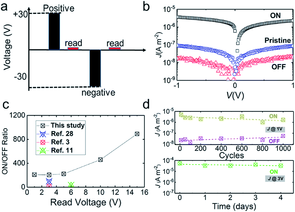 | ||
| Fig. 7 (a) Schematic illustration of the operation program for the ferroelectric nonvolatile memories, (b) current density (J)–voltage (V) characteristics of the blend LB nanosheets (P3CPenT 23 wt%, 40 layers) before and after polarization, (c) ON/OFF ratios at varying read voltage, and (d) (top) the device cycle endurance at ON- and OFF-states reading at 1 V and (bottom) the retention property at ON-state reading at 3 V. Dashed lines represent the linear fits at different states. | ||
In conclusion, a bottom-up construction of ferroelectric PVDF/semiconductive P3CPenT nanoblends was achieved simply by in situ mixing at the air–water interface. The PVDF matrix manifests ultrahigh ferroelectric crystal content, approaching 100% and guaranteeing the ferroelectricity necessary for the modulation of charge transfer and accumulation. Semiconductive P3CPenT components uniformly dispersed in PVDF matrix with some nanostructures such as particles and nanofibers. Ferroelectric nonvolatile memories based on the blend nanosheets were demonstrated with resistive switching properties along with the reversal of ferroelectric polarization direction. The ON/OFF ratio values and retention time are superior to most of the previously reported values, indicative of a great potential for application of such blend nanosheets to flexible electronics.
Conflicts of interest
There are no conflicts to declare.Acknowledgements
The work was supported by Grants-in-Aid for Scientific Research (B) (24350112) and for Young Scientists (16K17953) from the Japan Society for the Promotion of Science (JSPS). The work was also supported by the Research Program of “Dynamic Alliance for Open Innovation Bridging Human, Environment and Materials” in “Network Joint Research Center for Materials and Devices”. H. Zhu appreciates financial support from the Tohoku University Center for Gender Equality Promotion (TUMUG). Furthermore, the authors are grateful to Professor Hidetoshi Oikawa, IMRAM, Tohoku University, for the use of an X-ray diffractometer. Acknowledgment is also made of the Central Analytical Facility of IMRAM for providing the AFM instrument.Notes and references
- P. Heremans, G. H. Gelinck, R. Muller, K. J. Baeg, D. Y. Kim and Y. Y. Noh, Chem. Mater., 2011, 23, 341–358 CrossRef CAS.
- H. Zhu, S. Yamamoto, J. Matsui, T. Miyashita and M. Mitsuishi, J. Mater. Chem. C, 2014, 2, 6727–6731 RSC.
- K. Asadi, D. M. de Leeuw, B. de Boer and P. W. M. Blom, Nat. Mater., 2008, 7, 547–550 CrossRef CAS PubMed.
- K. Asadi, M. Li, P. W. M. Blom, M. Kemerink and D. M. de Leeuw, Mater. Today, 2011, 14, 592–599 CrossRef CAS.
- K. Asadi, T. G. de Boer, P. W. M. Blom and D. M. de Leeuw, Adv. Funct. Mater., 2009, 19, 3173–3178 CrossRef CAS.
- M. Li, N. Stingelin, J. J. Michels, M.-J. Spijkman, K. Asadi, R. Beerends, F. Biscarini, P. W. M. Blom and D. M. de Leeuw, Adv. Funct. Mater., 2012, 22, 2750–2757 CrossRef CAS.
- R. C. G. Naber, K. Asadi, P. W. M. Blom, D. M. de Leeuw and B. de Boer, Adv. Mater., 2010, 22, 933–945 CrossRef CAS PubMed.
- M. Kemerink, K. Asadi, P. W. M. Blom and D. M. de Leeuw, Org. Electron., 2012, 13, 147–152 CrossRef CAS.
- L. Nougaret, H. G. Kassa, R. Cai, T. Patois, B. Nysten, A. J. J. M. van Breemen, G. H. Gelinck, D. M. de Leeuw, A. Marrani, Z. Hu and A. M. Jonas, ACS Nano, 2014, 8, 3498–3505 CrossRef CAS PubMed.
- T. Braz, Q. Ferreira, A. L. Mendonça, A. M. Ferraria, A. M. B. do Rego and J. Morgado, J. Phys. Chem. C, 2014, 119, 1391–1399 Search PubMed.
- J. Hu, J. Zhang, Z. Fu, J. Weng, W. Chen, S. Ding, Y. Jiang and G. Zhu, ACS Appl. Mater. Interfaces, 2015, 7, 6325–6330 CAS.
- H. Zhu, M. Mitsuishi and T. Miyashita, Macromolecules, 2012, 45, 9076–9084 CrossRef CAS.
- H. Zhu, J. Matsui, S. Yamamoto, T. Miyashita and M. Mitsuishi, Soft Matter, 2015, 11, 1962–1972 RSC.
- T. Miyashita, Y. Mizuta and M. Matsuda, Br. Polym. J., 1990, 22, 327–331 CAS.
- J. Matsui, S. Yoshida, T. Mikayama, A. Aoki and T. Miyashita, Langmuir, 2005, 21, 5343–5348 CrossRef CAS PubMed.
- B. J. Worfolk, D. A. Rider, A. L. Elias, M. Thomas, K. D. Harris and J. M. Buriak, Adv. Funct. Mater., 2011, 21, 1816–1826 CrossRef CAS.
- W. Li, B. J. Worfolk, P. Li, T. C. Hauger, K. D. Harris and J. M. Buriak, J. Mater. Chem., 2012, 22, 11354–11363 RSC.
- B. Li, Y. Wu, M. Liu and A. R. Esker, Langmuir, 2006, 22, 4902–4905 CrossRef CAS PubMed.
- F. Monroy, F. Ortega and R. G. Rubio, Phys. Rev. E: Stat. Phys., Plasmas, Fluids, Relat. Interdiscip. Top., 1998, 58, 7629–7641 CrossRef CAS.
- H. M. Hilles, F. Ortega, R. G. Rubio and F. Monroy, Phys. Rev. Lett., 2004, 92, 255503 CrossRef PubMed.
- D. L. Thomas, L. J. Blum and A. P. Girard-Egrot, Biosens. Bioelectron., 2005, 20, 1539–1548 CrossRef CAS PubMed.
- L. Benedini, M. L. Fanani, B. Maggio, N. Wilke, P. Messina, S. Palma and P. Schulz, Langmuir, 2011, 27, 10914–10919 CrossRef CAS PubMed.
- R. Hasegawa, M. Kobayashi and H. Tadokoro, Polym. J., 1972, 3, 591–599 CrossRef CAS.
- M. Kobayashi, K. Tashiro and H. Tadokoro, Macromolecules, 1975, 8, 158–171 CrossRef CAS.
- Y. J. Shin, S. J. Kang, H. J. Jung, Y. J. Park, I. Bae, D. H. Choi and C. Park, ACS Appl. Mater. Interfaces, 2011, 3(2), 582–589 CAS.
- M. A. Khan, U. S. Bhansali, D. Cha and H. N. Alshareef, Adv. Funct. Mater., 2013, 23, 2145–2152 CrossRef CAS.
- L. S. Hung, C. W. Tang and M. G. Mason, Appl. Phys. Lett., 1997, 70, 152–154 CrossRef CAS.
- S. H. Sung and B. W. Boudouris, ACS Macro Lett., 2015, 4, 293–297 CrossRef CAS.
- A. Breemen, T. Zaba, V. Khikhlovskyi, J. Michels, R. Janssen, M. Kemerink and G. Gelinck, Adv. Funct. Mater., 2015, 25, 278–286 CrossRef.
- G. Zhu, Z. Zeng, L. Zhang and X. Yan, Appl. Phys. Lett., 2006, 89, 102905 CrossRef.
Footnote |
| † Electronic supplementary information (ESI) available: Materials, experimental details, and supplemental figures. See DOI: 10.1039/c8ra01143e |
| This journal is © The Royal Society of Chemistry 2018 |