
 Open Access Article
 This Open Access Article is licensed under a Creative Commons Attribution-Non Commercial 3.0 Unported Licence
Very fast hot carrier diffusion in unconstrained MoS2 on a glass substrate: discovered by picosecond ET-Raman†
Pengyu Yuan‡
 a,
Hong Tan‡b,
Ridong Wanga,
Tianyu Wanga and
Xinwei Wang§
*a
a,
Hong Tan‡b,
Ridong Wanga,
Tianyu Wanga and
Xinwei Wang§
*a
aDepartment of Mechanical Engineering, Iowa State University, Ames, IA 50011, USA. E-mail: xwang3@iastate.edu; Tel: +001-515-294-8023
bSchool of Energy and Power Engineering, Nanjing University of Science and Technology, Nanjing, Jiangsu 210094, China
First published on 3rd April 2018
Abstract
The currently reported optical-phonon-scattering-limited carrier mobility of MoS2 is up to 417 cm2 V−1 s−1 with two-side dielectric screening: one normal-κ side and one high-κ side. Herein, using picosecond energy transport state-resolved Raman (ET-Raman), we demonstrated very fast hot carrier diffusion in μm-scale (lateral) unconstrained MoS2 (1.8–18 nm thick) on a glass substrate; this method enables only one-side normal-κ dielectric screening. The ET-Raman method directly probes the diffusion of the hot carrier and its contribution to phonon transfer without contact and additional sample preparation and provides unprecedented insight into the intrinsic D of MoS2. The measured D values span from 0.76 to 9.7 cm2 s−1. A nonmonotonic thickness-dependent D trend is discovered, and it peaks at 3.0 nm thickness. This is explained by the competition between two physical phenomena: with an increase in sample thickness, the increased screening of the substrate results in higher mobility; moreover, thicker samples are subject to more surface contamination, loose substrate contact and weaker substrate dielectric screening. The corresponding carrier mobility varies from 31.0 to 388.5 cm2 V−1 s−1. This mobility is surprisingly high considering the normal-κ and single side dielectric screening by the glass substrate. This is a direct result of the less-damaged structure of MoS2 that is superior to those of MoS2 samples reported in literature studies that are subjected to various post-processing techniques to facilitate measurement. The very high hot carrier mobility reduces the local carrier concentration and enhances the Raman signal, which is further confirmed by our Raman signal studies and comparison with theoretical studies.
Introduction
Two-dimensional (2D) layered transition metal dichalcogenides (TMDs) have attracted significant research attention due to their potential applications in electronic and optical devices.1 Among TMDs, molybdenum disulfide (MoS2) is one of the most stable layered materials of this class. The thickness-dependent bandgap of MoS2 (1.3–1.8 eV)2,3 endows it with a broad range of diverse applications; especially, coating a silicon-based solar cell with the MoS2 film can greatly improve the efficiency of the cell.4 Additionally, MoS2-based field-effect transistors (FETs) have demonstrated very promising electronic characteristics such as high current on/off ratios (105–1010)5,6 and carrier mobilities (up to 410 cm2 V−1 s−1).7 With the rapidly increasing interest in the development of MoS2-based devices, determination of the intrinsic properties and the interface thermal energy coupling of MoS2 is of primary significance.8–10The interface thermal energy coupling of devices is a critical property because it determines their overall performance and lifetime.11,12 However, accurate and straightforward measurement of this property is still very challenging due to the involvement of many different complicated physical phenomena.13,14 Both theoretical and experiment-based methods have been developed and successfully applied to characterize interface thermal energy coupling. Theoretical studies use the acoustic/diffuse mismatch model15,16 and molecular dynamics simulations.12 Experiment-based methods include the pump-probe technique17 and Raman-based thermal probing technique.12 Additionally, for semiconductor materials under an electrical field or light excitation, the generated hot carriers can significantly contribute to thermal diffusion in electronic devices.11 Similar to free electrons in metals, hot carriers can diffuse in semiconductor materials; therefore, their movement is strongly affected by various interactions between the carriers and other excitations.6 By studying hot carrier diffusion, we can obtain a deeper understanding of the scattering process and energy distribution in semiconductors.18 For MoS2, most work has focused on measuring its mobility, in which the carrier is generated under an electric field and the sample is covered by a top-gate or connected to the electric contact to form FETs.6,19 However, these treatments are still believed to provide inaccurate or overestimated results.20 One possible reason is that the sample may be modified during the device preparation process.21,22 Therefore, by studying carrier transport without applying an electric field and with proper use of a dielectric substrate, the intrinsic properties of MoS2 nanosheets can be obtained. Accordingly, optical-based measurements of the transport properties of hot carriers are preferred, such as transient absorption microscopy,23 spatially and temporally resolved pump-probe techniques,24 and Raman-based techniques.11
Currently, silicon wafer is a very popular substrate for standard integrated circuit processing; it is ideal for creating transistors due to its extreme uniformity and good chemical and mechanical strength.25 Therefore, tremendous work has focused on the study of semiconductor materials supported on silicon substrates, such as graphene,26 TMDs,12 and black phosphorus.27 However, in other applications, such as display pixel backplanes and peripheral logic devices,28,29 glass or plastic substrates are more recommended. For MoS2 supported on glass substrates, a few related studies have been reported; however, these are limited to simple FET structures.30–32 From another aspect, the mechanical properties of MoS2 nanosheets can be strongly affected by the properties and morphology of the substrate. Unlike the polished c-Si substrate we used in our previous work,33 MoS2 prepared through mechanical exfoliation onto a glass substrate does not follow its nanoscale rough surface but instead is supported by the high points on the substrate. This surface roughness affects the energy coupling of MoS2 nanosheets and the substrate; therefore, it may cause a local variance in the electrical and mechanical properties of a sample.34,35 Tang et al. indicated that loose contact at an interface can significantly increase the thermal resistance of the interface.36 Also, a large temperature increase in glass substrates is expected in experiments due to its relatively low thermal conductivity.37 However, the temperature profiles of glass substrates cannot be obtained by Raman spectroscopy because there is no prominent Raman spectrum in most glass substrates. Additionally, compared with c-Si substrate, the greater dielectric effect from the glass substrate (SiO2) can dramatically increase the carrier diffusion coefficient of its supported MoS2 nanosheets.38–40 Due to these additional considerations when using glass instead of Si as a substrate, it is very challenging and complicated to study MoS2 nanosheets supported on glass substrates.
Here, before reporting our current work, we would like to outline the significant advances we reported in each of our three previous studies published on 2D MoS2 to demonstrate the significance and discovery of the current work. In the first study,41 for the first time, we reported the dependence of the thermal resistance/conductance of the MoS2/c-Si interface on the thickness of the 2D nanofilm and provided a rigorous analysis of the effects of Si laser absorption on the interface structure. Later during our extensive study, as reported in the second publication,11 we discovered that hot carrier generation, diffusion, and recombination can play vital roles in in-plane and cross-plane energy transfer in the MoS2/c-Si interface system. Furthermore, the effects of hot carrier diffusion on interface thermal energy transport had rarely been studied. Therefore, we designed a novel technique and a new physical model to characterize hot carrier diffusion and thermal transport at the MoS2/c-Si interface. This is the first consideration of this conjugated transfer and represented the most advanced study at that time. In the above two studies, the optical properties of the materials are need-to-know parameters to evaluate the laser absorption rates. This evaluation can induce considerable uncertainties and unknown errors due to variation between samples and interface optical interference.2,42,43 Additionally, it is necessary to obtain the Raman wavenumber temperature coefficient to evaluate the absolute temperature increase of a sample. This results in very large errors, as reported for all previous Raman-based measurements.44–46 In fact, studies on MoS2 interface thermal resistance by different groups worldwide have reported results with substantial deviations which cannot be simply explained by differences in sample structure. Therefore, we developed an entirely new technique independent of laser-absorption evaluation and Raman-temperature calibration to provide the most accurate characterization to date. This was reported in our third study,33 where an energy transport state-resolved Raman (ET-Raman) technique was developed using CW and picosecond Raman with consideration of both in-plane hot carrier diffusion and interface energy coupling. This is the best Raman-based technique to date to characterize 2D material energy transfer. We expect that this technique will have a long-term profound impact, like the pump-probe technique, in characterizing thermal and charge carrier transfer in extremely thin structures. The reason that we are still using MoS2/c-Si is to compare our results with previous results for both technique verification and uncertainty analysis.
In this work, the advanced ET-Raman technique is applied to study six mechanically exfoliated MoS2 nanosheet samples (thickness from 1.8 nm to 18 nm) supported on glass substrate. We discovered high-end hot carrier diffusivity which is comparable to that of MoS2 sandwiched between very high-κ dielectric materials. Considering the low-κ glass substrate and its single-side dielectric screening, our reported high-end hot carrier diffusion is unexpectedly high and has never been reported before. Furthermore, variation of the nonmonotonic hot carrier diffusivity with MoS2 thickness is revealed and explained by the different physical phenomena affecting the diffusivity. This indicates new methods of fabricating novel MoS2-based devices with high mobility via control of the substrate type and sample thickness. For substrate materials with low thermal conductivity (e.g. the glass used in this work), our originally developed ET-Raman technique has been re-designed to include two picosecond laser heating states and to use their differential to rule out long-term heat accumulation and unknown thermal response of the substrate because no Raman signals are provided.
Physical principles of picosecond ET-Raman
In ET-Raman, different energy transport states are constructed in both space and time domains to examine the thermal response of a sample. Fig. 1(a) shows the physical principles of this technique. Hot carriers will be generated when the photon energy is larger than the bandgap of MoS2. With additional energy ΔE = (E − Eg), the hot carriers (electrons) are unstable and will lose energy by a fast thermalization process (∼0.5 to 1 ps). Then, the remaining photon energy (Eg) will be carried by the carriers. They take this energy and diffuse out of the excitation area until they recombine with holes to release the energy to local phonons. Therefore, the real heating area will be expanded due to the hot carrier diffusion. By using Raman spectroscopy, we can probe the different temperature profiles of a sample. Note that for glass substrates, no hot carriers are generated and the surface recombination of MoS2 will be strongly restricted due to the dielectric effect of the substrate. The energy of the phonons in the MoS2 nanosheets will dissipate within the sample and through the layers down to the glass substrate to increase the local temperature.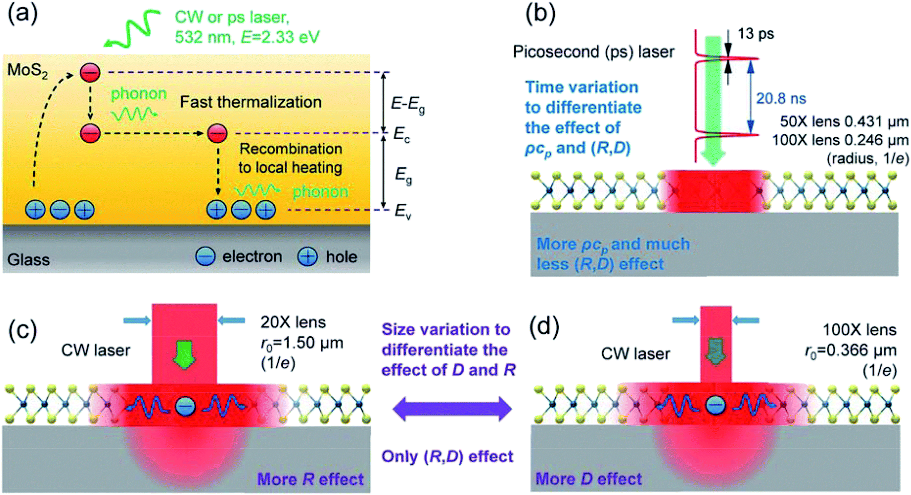 | ||
| Fig. 1 (a) Schematic of MoS2 under laser excitation (not to scale). In the MoS2 sample, hot carriers are generated by photons (2.33 eV) while exciting electrons (e) to the conduction band (Ec), leaving holes (h) in the valence band (Ev). Through a fast thermalization process (∼0.5 to 1.0 ps), hot carriers transfer part of the photon energy (E − Eg) to phonons, then diffuse out of the direct laser heating region to the low population region. Finally, they recombine with holes and lose their remaining photon energy (Eg) through phonon emission (carrier-phonon scattering). (b)–(d) An artistic representation of the experiment concept. A 532 nm continuous-wave (CW) or picosecond (ps) laser simultaneously heats and probes the temperature increase to generate four different energy transport states in space and time domains. (b) ps laser (pulse width is 13 ps, pulse period is 20.8 ns) heating under 100× and 50× objectives. No e–h recombination occurs within the short pulse time, and heat conduction from the heating region is negligible. The temperature increase is determined by the volumetric heat capacity (ρcp) of the sample, with less effect from (R, D). (c) and (d) Two objective lenses (20× and 100×) of the CW laser are used to realize different laser spot sizes; heating with simultaneous Raman probing is used to detect the local temperature increase to study the (R, D) effects. (c) Laser heating under the 20× objective. The radius of the laser spot size is around 1.50 μm (1/e profile). (d) The laser heating spot size is reduced using the 100× objective. The radius is around 0.366 μm (1/e profile). | ||
We generated two sub-states for steady-state heating with different laser heating sizes. As shown in Fig. 1(c) and (d), we used a CW laser source to study the temperature profile with only the (R, D) effects. Different objective lenses (100× and 20×) were used to differentiate the effects of D and R. The laser spots have radii of 1.50 μm and 0.366 μm (1/e profile) for the 20× and 100× objectives, respectively. The absorbed laser energy in MoS2 nanosheets will be conducted directly to the substrate via R and to the in-plane direction, then to the substrate through the interface with effects from both R and D. The same laser beam will excite the Raman signal of the sample, which can then be collected to analyze the temperature profile. By collecting and analyzing the Raman signals under different laser powers (P), we can obtain the Raman shift power coefficient (RSC): χCW = ∂ω/∂P. Two RSC values can be obtained for each sample by varying the objective objectives: χCW1 for the 20× objective, χCW2 for the 100× objective. Note that the temperature mentioned here is actually represented by RSC because we do not need to determine the absolute temperature increase when using the ET-Raman technique.
Then, we generated two zero-transport states by applying a ps laser (532 nm, the pulse duration is 13 ps, the repetition rate is 48.2 MHz), as shown in Fig. 1(b). Similarly, we obtained RSC under both 50× and 100× objectives as χps1 and χps2, respectively. Within each pulse (13 ps), the thermal diffusion lengths for the MoS2 nanosheets and glass substrate were around 38 nm and 6.6 nm, respectively. (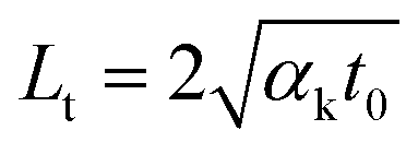 , αk = 2.75 × 10⁻⁵ m2 s−1 for MoS2 for the in-plane thermal diffusivity, and 8.26 × 10⁻⁷ m2 s−1 for glass;47 t0 = 13 ps is the ps laser pulse width). These are all much smaller than the laser spot size (r0 is 0.246 μm for the 100× objective and 0.431 μm for the 50× objective). Hence, the heat conduction in the laser heating region has a very weak effect on the temperature increase. The relaxation time of the MoS2 nanosheets supported on a glass substrate (R ∼ 10−6 K m2 W−1) can be estimated as δzρcpR = 37.8 ns. When the thickness of MoS2 δz is 10 nm, its volumetric heat capacity ρcp = 1.89 MJ m−3 K−1; when the interface thermal resistance R is 2 × 10⁻⁶ K m2 W−1, the relaxation time is even longer than the ps laser cooling time (20.8 ns). Therefore, the sample cannot be fully cooled to its original temperature. Instead, it is heated again when the next pulse comes until the sample reaches thermal equilibrium with the environment. Hence, there is a steady-state heat accumulation effect, as shown in Fig. 2(b). As a result, the temperature increase (χps) arises from the combined effects of a single pulse and the steady-state accumulation of heat. Especially, the effect of the heating amount on the steady-state accumulation is negligible. Therefore, the temperature increase induced by accumulation is almost identical under the same laser power level (e.g., 1 mW) when thermal equilibrium is reached. However, the temperature increase from a single pulse mostly arises from the volumetric heat capacity of the sample (ρcp) and will be different for different heating sizes. By comparing the zero-conduction states under different heating sizes (100× and 50× objectives), we could eliminate the steady-state accumulation effect. As a result, we could use these zero-transport states (ps laser heating) to distinguish the roles of ρcp and (R, D) with a negligible contribution of D and R to the temperature increase.
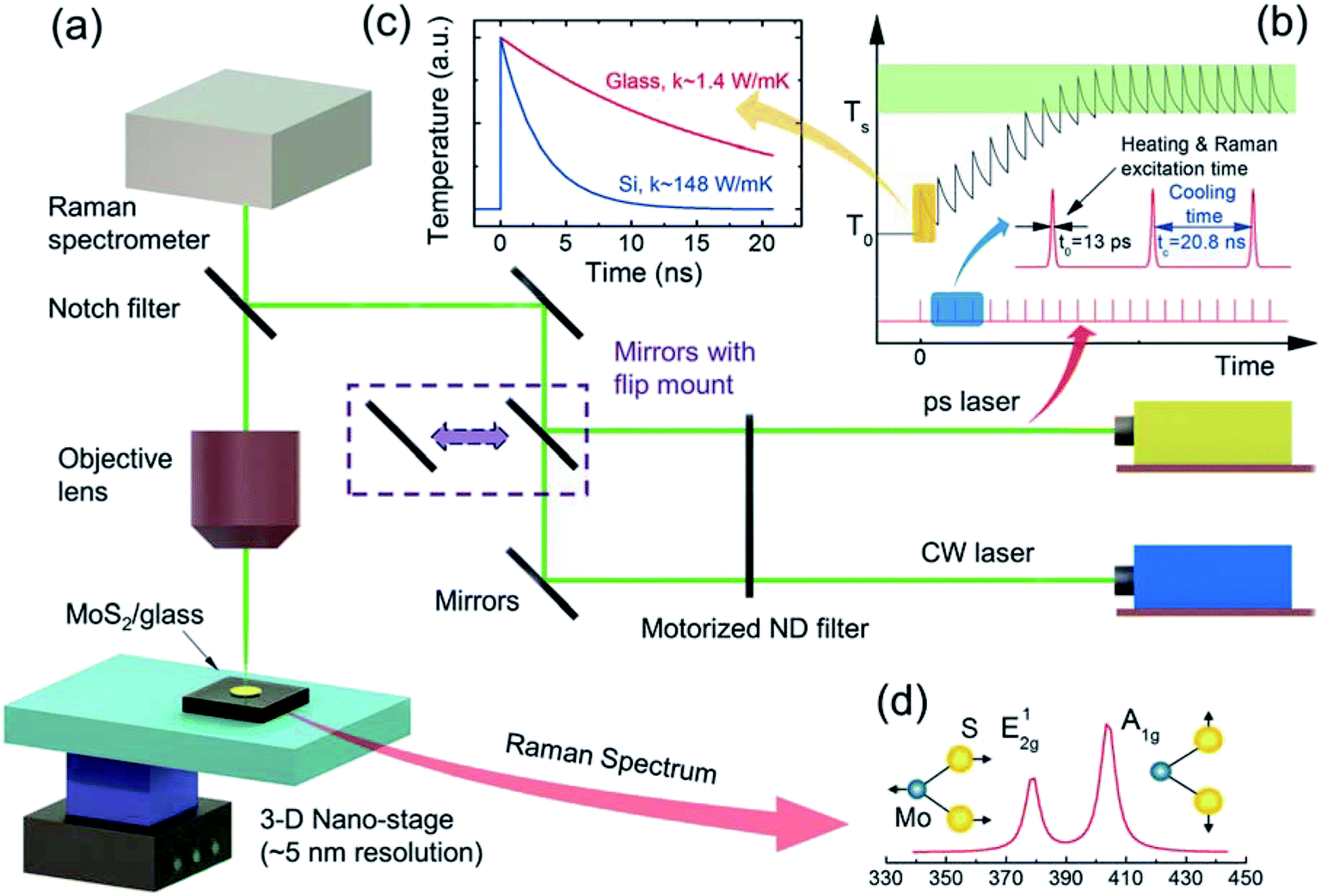 | ||
| Fig. 2 (a) Schematic of the ET-Raman experiment setup. A typical MoS2/glass sample is mounted on a 3D nano-stage and illuminated by CW and ps 532 nm lasers, which can be switched by the flip-mounted mirror. The same laser is used to excite the Raman signals, which are collected by a confocal Raman spectrometer (Voyage, B&W Tek, Inc.). The laser power is adjusted using a motorized ND filter. (b) The ps laser has a pulse width of around 13 ps, and the repetition rate is 48.2 MHz (cooling time is 20.8 ns). For our MoS2-on-glass structure, the temperature cannot be cooled completely to the original temperature (T0) before the next pulse comes. Therefore, there is a steady-state heat accumulation effect. (c) Compared with Si substrate, glass has a much smaller thermal conductivity (k ∼ 1.4 W m−1 K−1); therefore, its temperature cannot decay to its original state before the next pulse comes. (d) Raman spectra of MoS2 in an ambient air environment. The temperatures of MoS2 can be determined from the Raman spectra. E12g (∼383 cm−1), A1g (∼408 cm−1) modes were observed in our six samples. Here, we chose the E12g mode to evaluate the MoS2 temperature profile. | ||
For the MoS2 nanosheets on glass substrate, after the steady-state and zero-transport heating experiments, we defined the dimensionless normalized RSC as Θ1 = χCW1/(χps2 − χps1) and Θ2 = χCW2/(χps2 − χps1). Notably, this normalized RSC completely rules out the effects of laser absorption, Raman temperature coefficients, and the pulse accumulation effect. Θ1 and Θ2 are functions only of the 2D material and the ρcp, R, and D of the substrate materials. Using a 3D heat conduction model that includes all these properties, we could finally determine D and R of the 2D material. Consequently, using ET-Raman, the uncertainties from the evaluations of the absorbed laser power level and absolute temperature increase could be eliminated.
Physical model and governing equations for data processing
For the steady-state heating, we used two partial differential equations to express the generation and diffusion of heat and electrical carriers in the sample in cylindrical coordinates:48,49
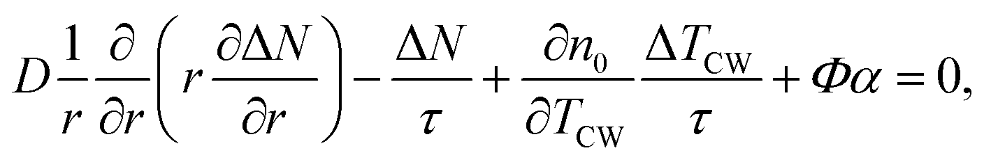 | (1) |
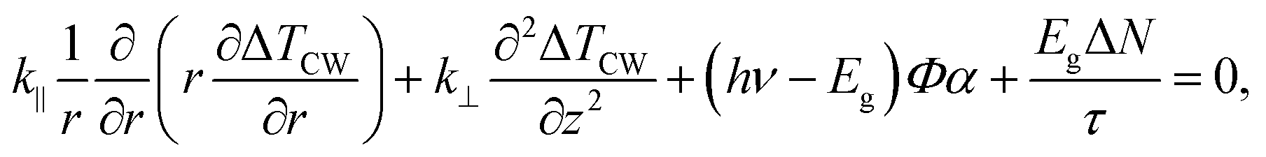 | (2) |
The hot carrier diffusion can significantly extend the heated area, especially when the laser heating spot size (radius: 0.366 μm to 1.50 μm) is comparable to or smaller than the carrier diffusion length (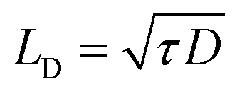 , ∼0.1 μm for few-layered MoS2 (ref. 5 and 51)). Otherwise, the hot carrier diffusion will have a small or negligible effect on the heating area.
The zero-transport heating states only consider the fast thermalization process because the ps laser pulse (13 ps) is so short that we do not need to consider the hot carrier recombination process. Additionally, the hot electrons and holes will cool quickly (∼0.5 to 1.0 ps), and the thermalization can be assumed to occur instantly in our process. As a result, for picosecond laser excitation, we can apply a single temperature to evaluate the fast thermalization process. By only considering the laser absorption in the MoS2 sample, we have
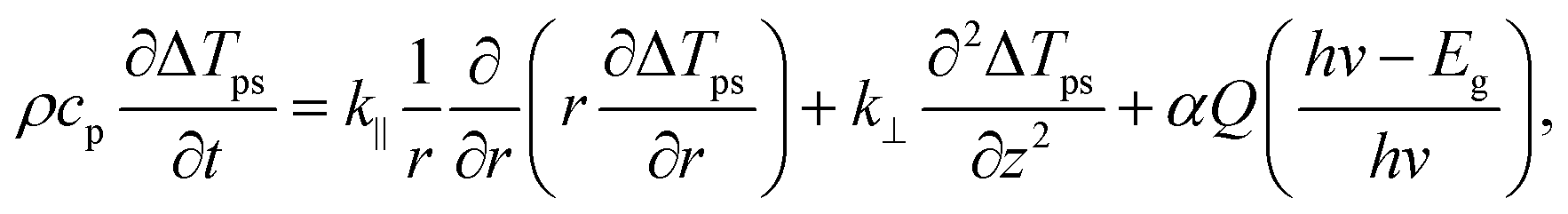 | (3) |
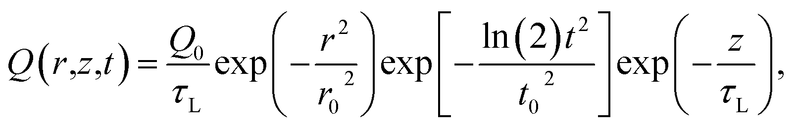 | (4) |
In brief, under steady-state heating, the measured temperature increase of MoS2 is determined by the hot carrier diffusion coefficient and the thermal resistance of the interface. Under zero-transport state heating, the temperature increase difference for the two heating sizes [ΔTps(100×) − ΔTps(50×)] is only determined by the laser absorption and ρcp. By solving eqn (1)–(4), we can rule out the laser absorption term and deduce the ratio of the temperature increase (the normalized RSC) ![[T with combining macron]](https://www.rsc.org/images/entities/i_char_0054_0304.gif) CW/[ps(100×) − ps(50×)] of the sample from two heating states. Then, we can solve eqn (1) and (2) to analyze the experimental results and determine the hot carrier diffusivity and the interface thermal resistance. Note that the above governing equations consider both MoS2 and glass. The heat flow continues through the MoS2/glass interface; however, the temperature is discontinuous because of the non-ideal contact. Therefore, their temperature difference was determined and used.
CW/[ps(100×) − ps(50×)] of the sample from two heating states. Then, we can solve eqn (1) and (2) to analyze the experimental results and determine the hot carrier diffusivity and the interface thermal resistance. Note that the above governing equations consider both MoS2 and glass. The heat flow continues through the MoS2/glass interface; however, the temperature is discontinuous because of the non-ideal contact. Therefore, their temperature difference was determined and used.
Fig. 2 shows a schematic of the Raman experiment setup (see ESI S1† for more details), which is the same as the one we used to study MoS2 nanosheets on c-Si substrates.33 In both the steady-state and zero-transport heating experiments, the laser beam is focused on a specific area of the samples (as shown in Fig. S1†). The temperature response of MoS2 can be evaluated by analyzing the Raman spectrum. Fig. 2(d) shows two prominent Raman peaks of MoS2: the in-plane (E12g) mode located around 383 cm−1 and the out-of-plane (A1g) mode located at around 408 cm−1.52
In this work, we prepared six few-layered MoS2 samples supported on glass substrates using a micromechanical exfoliation technique (see ESI S2† for more details). Through AFM (atomic force microscopy) measurements, we determined the thicknesses of the six samples to be 1.8 nm, 3.0 nm, 5.4 nm, 7.8 nm, 11.4 nm, and 18 nm. To obtain a better idea of the uniformity of the surface structures of the samples, we also performed Raman shift mapping using a CW laser line for the 3.0 nm and 7.8 nm thick MoS2 samples (see ESI S2† for more details). The roughness of a sample can significantly affect the laser absorption rate. However, by using ET-Raman, the uncertainty from the evaluation of laser absorption can be eliminated. The roughness itself can affect the interface energy coupling and therefore increase the thermal resistance of the interface.
Thermal response of MoS2 under CW and ps laser heating
For both steady-state and zero-transport state Raman experiments, eight room-temperature Raman spectra were collected at different laser powers by the control computer to determine the laser power coefficient for each sample. The CW laser energy was varied from 0.38 mW to 2.13 mW (0.090 to 0.506 MW cm−2) under the 100× objective and from 1.34 to 7.59 mW (0.019 to 0.107 MW cm−2) under the 20× objective. The ps laser energy was varied from 0.195 to 1.106 mW (pulse power density is 0.053 to 0.303 GW cm−2) under the 50× objective and from 0.126 to 0.611 mW (pulse power density is 0.106 to 0.514 GW cm−2) under the 100× objective. Note that this laser power represents the level just before the laser enters the surface of the MoS2 sample; it is kept as low as possible to avoid heat-induced damage to the sample,11 which can also lead to broadening and shifting of the Raman peaks. Especially for ps laser Raman, photon absorption saturation must be avoided and the sample must be maintained within the linear temperature dependence range of its Raman properties.53,54 For the 532 nm picosecond pulse laser heating, the saturation intensity was around 1.13 GW cm−2.54 When the photon density exceeds that level, the conductance band will be filled and the material will be unable to absorb further photons according to the Pauli exclusion principle.55 For the 1.8 nm thick MoS2 under 100× objective with ps laser, we found that the saturable absorption began around 0.602 GW cm−2, which is lower than the saturation intensity from the literature. Therefore, the saturation intensity for different samples may vary slightly, and very careful selection of the laser power range is necessary.Next, we take the 1.8 nm thick sample to illustrate the results of this work. Fig. 3(a) shows five representative room temperature Raman spectra and their corresponding Lorentzian fits of MoS2 under the 100× objective by CW laser. The results under the 50× objective by ps laser are shown in Fig. 3(b). In Fig. 3(a), with increasing laser power, both modes of MoS2 shift linearly to the left (red shift); the shifts are visible as Δω|(0.38 mW–2.13 mW) by CW laser and Δω|(0.19 mW–1.11 mW) by ps laser for MoS2. These Raman shift changes show that the temperature of the sample heating area increases under a higher laser power. Note that the Raman linewidth of MoS2 from the CW laser is smaller than that from the ps laser, as shown in Fig. 3(a) and (b). This is because the observed Raman signal is not solely dependent on the spectral resolution of the spectrometer, but is also dependent on the linewidth of the laser. The CW laser has a spectral linewidth of less than 0.01 pm. However, the picosecond laser has a linewidth of around 9 pm. However, this will not affect the absolute Raman peak position. Additionally, we used the linear fitting results from the Raman shift position against the laser power to determine the final results. Therefore, the absolute difference in Raman spectra from the two laser sources can be ruled out.
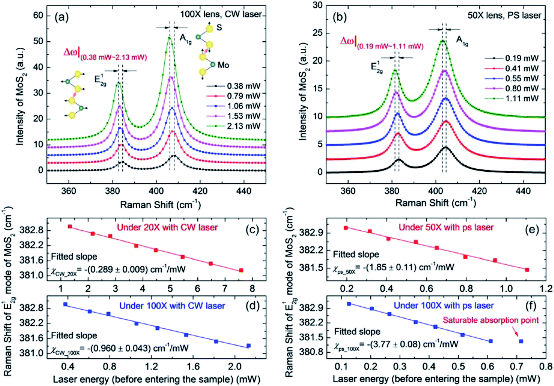 | ||
| Fig. 3 Raman spectra of the MoS2 nanosheets. The sample with a thickness of 1.8 nm is used here to illustrate the ET-Raman experiment results. Two different objective lenses were used to generate different laser heating phenomena and different laser sources were used to generate different energy transport states. The local temperature increases when the laser power increases for both the CW laser and ps laser. (a) Five representative Raman spectra of MoS2 at increasing excitation laser power under the 100× objective with the CW laser in the ambient environment. Here, we shifted the spectra to improve the clarity for both (a) and (b). By CW laser, the Raman shifts for the two modes of MoS2 are visible as Δω|(0.38 mW–2.13 mW) in (a). The Raman shifts for the E12g mode of MoS2 as a function of laser power under the 20× objective and the 100× objective are shown in (c) and (d), respectively. The fitting results (solid lines) for the linear power coefficient χP are shown in these figures. (b) Five representative Raman spectra of MoS2 at increasing excitation laser power under the 50× objective with the ps laser in the ambient environment. The Raman shifts for two modes of MoS2 with the ps laser are visible as Δω|(0.19 mW–1.11 mW) in (b). The Raman shifts for the E12g mode of MoS2 as a function of laser power under the 50× and 100× objectives with the ps laser are shown in (e) and (f), respectively. | ||
Different optical heating phenomena can be generated by applying two objective objectives with the CW laser. In our specified laser power range for both the CW and ps lasers, the Raman shift linearly depends on the laser power by Δω = ω(P2) − ω(P1) = χ(P2–P1) = χΔP. χ (cm−1 mW−1) is the first-order Raman shift power coefficient (RSC) for the two vibration modes of MoS2, and P (mW) is the laser power. Here, Raman results from this E12g vibration mode were chosen and used to deduce RSC considering the effects from the interlayer interactions and the effects of the substrate for A1g mode.56 Additionally, the effects of switching laser sources on the Raman results can also be eliminated by choosing E12g mode due to its weak polar dependence on the laser polarization configuration. Using the CW laser, as shown in Fig. 3(c) and (d), the linear fitting RSC result for MoS2 E12g mode under the 20× objective (χCW1) is −(0.289 ± 0.009) cm−1 mW−1, and that under the 100× objective (χCW2) is −(0.960 ± 0.043) cm−1 mW−1. χCW2 is larger than χCW1 because the temperature increases more rapidly under the 100× objective due to its larger power density (smaller laser spot size). Additionally, these values are much higher than the corresponding RSC (CW) values of MoS2 (6.6 nm thick) on c-Si substrate: −0.026 cm−1 mW−1 (20× objective) and −0.150 cm−1 mW−1 (100× objective).33 For the glass substrate, the heat dissipation is less efficient due to its low thermal conductivity. Therefore, a larger temperature increase is expected for MoS2 supported on glass substrate. Using the ps laser under the 50× and 100× objectives, as shown in Fig. 3(e) and (f), the RSC values of MoS2 in E12g mode are −(1.85 ± 0.11) cm−1 mW−1 and −(3.77 ± 0.08) cm−1 mW−1, respectively. The power coefficient under the 100× objective (χps2) is larger than that under the 50× objective (χps1). This difference arises from the temperature increase from a single pulse. As with CW laser heating, the ps laser under the 100× objective has a higher power density. Similarly, for the 50× objective, the RSC (ps) value is also much higher than the corresponding value of MoS2 (6.6 nm thick) on c-Si substrate (−0.057 cm−1 mW−1).33 We also summarized the RSC values for all six samples in Table S1 (see ESI S3†). The RSC roughly increases with the sample thickness for both CW and ps laser heating. When the sample thickness is smaller than its laser absorption depth, the thicker sample will absorb more energy and a higher temperature increase is expected. As a result, the Raman wavenumber change will increase under the same laser power level.
Determination of D and R
We applied 3D numerical modeling based on the finite volume method to calculate the temperature increase to determine the D and R values. Detailed information for the modeling is provided in the experimental section. Taking 1.8 nm thick MoS2 as an example, from the 3D numerical simulation and Raman experiment, we can calculate the normalized RSC values (Θ1 and Θ2) for MoS2 in the (D, R) space. Fig. 4(a) and (b) show the calculated normalized RSC mapping for MoS2. Many different (D, R) pairs can satisfy the experimental normalized RSC (the isolines). By combining the results from these two cases, as shown in Fig. 4(c), we can determine the exact D and R values from the cross point of the blue (Θ1) and dark red (Θ2) dashed curves: D is 4.17 cm2 s−1, and R is 1.28 × 10⁻⁶ K m2 W−1. The normalized probability distribution function (Ω) is used to present the uncertainty of the final result, as shown in the false color map of Fig. 4(c). Ω = exp[−(x −![[x with combining macron]](https://www.rsc.org/images/entities/i_char_0078_0304.gif) )2/(2σ2)], where x, , and σ are the variable, its average, and the standard deviation, respectively. In the (D, R) space, we have Ω(D,R) = ΩΘ1ΩΘ2. We used the value of Ω(D,R) = 0.6065 corresponding to the σ confidence in the (D, R) space to evaluate the uncertainty of the final results. Finally, the deduced R is 1.28+0.16−0.16 × 10⁻⁶ K m2 W−1, and D is 4.17+1.33−0.97 cm2 s−1. The final results with the uncertainties for all six samples are summarized in Table 1 and are also plotted in Fig. 5(a) and (b).
)2/(2σ2)], where x, , and σ are the variable, its average, and the standard deviation, respectively. In the (D, R) space, we have Ω(D,R) = ΩΘ1ΩΘ2. We used the value of Ω(D,R) = 0.6065 corresponding to the σ confidence in the (D, R) space to evaluate the uncertainty of the final results. Finally, the deduced R is 1.28+0.16−0.16 × 10⁻⁶ K m2 W−1, and D is 4.17+1.33−0.97 cm2 s−1. The final results with the uncertainties for all six samples are summarized in Table 1 and are also plotted in Fig. 5(a) and (b).
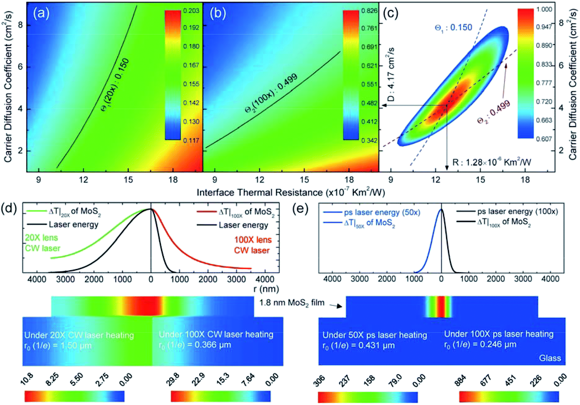 | ||
| Fig. 4 3D numerical modeling results for the 1.8 nm thick MoS2 sample. The normalized RSC (Raman shift power coefficient) Θ for different values of the hot carrier diffusivity and interface thermal resistance are shown in (a) under the 20× objective and in (b) under the 100× objective. The experimentally obtained Θ1 = 0.150 and Θ2 = 0.499 are shown in these two figures. (c) The determined D and R values as well as the uncertainty region. The normalized probability distribution function (Ω) contour gives the uncertainty distribution: 0.6065 for the σ confidence. Based on the determined D and R for this sample, the calculated temperature increase distributions and laser energy distributions in the 1.8 nm MoS2 sample with CW laser heating under the 20× and 100× objectives are shown in (d); those with ps laser heating with the 50× and 100× objectives are shown in (e). | ||
| Sample thickness | D (cm2 s−1) | μ (cm2 V−1 s−1) | LD (nm) | R (10−6 K m2 W−1) |
|---|---|---|---|---|
| 1.8 nm | 4.17+1.33−0.97 | 166.8+53.3−39.1 | 645.8+365.1−312.6 | 1.28+0.16−0.16 |
| 3.0 nm | 9.71+1.89−1.57 | 388.5+75.5−62.8 | 985.5+434.4−396.2 | 1.94+0.18−0.17 |
| 5.4 nm | 5.17+1.90−0.70 | 206.8+75.9−28.0 | 719.0+435.5−264.7 | 1.16+0.15−0.15 |
| 7.8 nm | 2.33+1.09−0.79 | 93.3+43.4−31.4 | 482.9+329.4−212.9 | 2.07+0.31−0.29 |
| 11.4 nm | 0.76+0.45−0.32 | 30.2+18.1−13.0 | 274.9+212.9−180.2 | 7.09+0.14−0.13 |
| 18.0 nm | 0.78+0.38−0.25 | 31.0+15.2−10.0 | 278.5+194.8−158.2 | 0.41+0.14−0.13 |
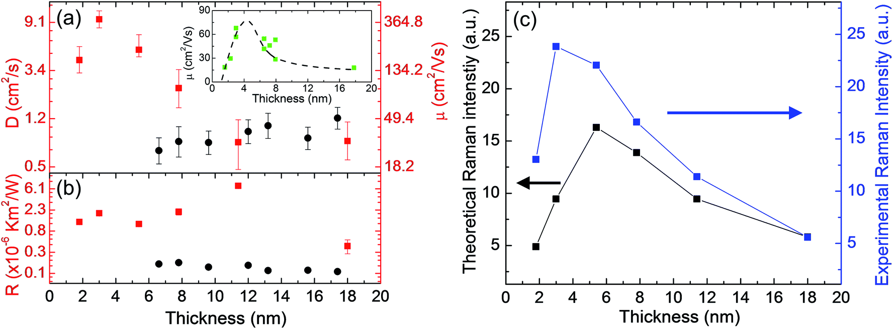 | ||
| Fig. 5 (a) Hot carrier diffusion coefficient (D) and (b) interface thermal resistance (R) versus sample thickness of six MoS2 samples on glass substrate (the red plots). The dark plots, included for comparison, are the corresponding D and R results from MoS2 samples supported on c-Si substrate from our previous work.33 The inset in Figure (a) shows the carrier mobility results from Lin et al.'s work at room temperature. The dashed dark line is a guide for the eye.62 (c) Comparison of the experimental Raman peak intensity trends of MoS2 E12g mode and the theoretical Raman intensity F for the six samples. | ||
Then, we obtained the temperature profile from the 3D modeling (by the determined D and R) for the 1.8 nm thick MoS2 sample and its substrate under the 20× (left part) and 100× (right part) objectives with CW laser heating. As shown in Fig. 4(d), this visualizes the effects of hot carrier diffusion on the thermal energy distribution. The temperature increase is quite uniform with increasing thickness due to the large lateral/vertical size ratio of the MoS2 nanosheets. Especially, the temperature increase in glass results from the thermal energy transferred from the upper MoS2. The low thermal conductivity of glass restricts the heat dissipation. Compared with the laser energy distribution (dark curve), the temperature distribution of MoS2 is far outside the laser spot, especially for the small heating size (100× objective). This is because the diffusion length LD (646 nm for 1.8 nm thick MoS2) is 1/2 of r0 under the 20× objective (1.5 μm) and almost twice that size under the 100× objective (366 nm). Therefore, the effect of hot carrier diffusion on heat conduction is more prominent under the 100× objective. To model the zero-transport state ps laser heating, we only considered the temperature increase from the single pulse. As shown in Fig. 4(e), the temperature increase of MoS2 has almost the same distribution as the ps laser energy. This confirms that R and D have negligible effects on the temperature increase of the samples. The temperature increase of the glass substrate is close to zero due to negligible heat transport from MoS2 during the very short ps laser pulse duration.
During the diffusion process of the carriers, electrons (e) and holes (h) move as units because of Coulomb attraction. Additionally, in this optical study, equal numbers of electrons and holes were generated, and their effective masses were comparable and even similar.57 Therefore, the measured value D can be treated as the unipolar carrier diffusivity of both electrons and holes. Additionally, the diffusivity is related to the mobility (μ) by the Einstein relation in this thermalized system, D/kBT = μ/q, where kB, T, and q are the Boltzmann constant, temperature, and the amount of charge of each carrier. Here, we assume that the carriers have a thermal distribution of 300 K during the diffusion process due to the ultra-short energy relaxation process (only several picoseconds).58 As a result, our measured D corresponds to a mobility range from 31.0 cm2 V−1 s−1 (18.0 nm thick) to 388.5 cm2 V−1 s−1 (3.0 nm thick). Carrier mobilities of 30 to 60 cm2 V−1 s−1 for few-layered MoS2 on SiO2 (ref. 39) and ∼70 cm2 V−1 s−1 for few-layered MoS2 on Al2O3 (ref. 59) were reported previously; these values are in excellent agreement with our lower bound measurement results. Our upper bound measurements are larger than those in most reported work. We attribute this to the fact that our MoS2 samples are unprocessed and unconstrained. Early electrical measurements deduced motilities in the range of 100 to 260 cm2 V−1 s−1 for bulk MoS2 crystals.51 Moreover, the theoretical optical-phonon-scattering-limited mobility was reported up to 400 cm2 V−1 s−1 by adopting high-κ dielectric materials (e.g., HfO2, Al2O3) to build top-gated devices.5,7,19,60 Furthermore, compared with the c-Si substrate (p-doped) we used in our previous work,33 the insulator glass substrate used in this work can create a better dielectric environment to enhance the dielectric screening of Coulomb potentials, which can lead to enhanced carrier mobility, especially for relatively thin MoS2 samples.39,40 Additionally, compared to air (dielectric constant is 1), MoS2 has a much larger dielectric constant (∼4).61 As a result, for thicker MoS2 samples, the upper part itself can also serve as a high dielectric environment (dielectric capping effect).39
Effects of MoS2 thickness on R and D
To determine the effects of the MoS2 thickness on the interface energy coupling and hot carrier transport, we ploted them as a function of MoS2 thickness, as shown in Fig. 5. For comparison, the D and R results from MoS2 supported on c-Si substrate from our previous work are also plotted in these two figures. Table 1 also lists all the results. The uncertainties of R and D mainly arise from the RSC fitting procedure. For the hot carrier diffusion coefficient D, as shown in Fig. 5(a), the 3.0 nm MoS2 sample has the largest value. Similar trends for this thickness-dependent carrier mobility were reported previously.40,62 The inset of Fig. 5(a) shows the carrier mobility results from Lin et al.'s work.62 They attribute their results to the effects of the metal source/drain contacts; only the top MoS2 layer could be connected to the contacts in their work.63 With decreasing sample thickness, the absence of sufficient screening of the substrate results in lower mobility. However, when the thickness decreases, the finite interlayer conductivity (in a resistor network model) can result in an effective higher total mobility.63 The competition of these two physical aspects accounts for the maximum mobility value at a certain layer thickness.64 For our optically generated hot carrier transport, the resistor network model does not apply. Instead, we provide the following explanations for this nonmonotonic relationship between the sample thickness and hot carrier diffusivity. For thin samples (1.8 nm and 3.0 nm thick), with increasing film thickness, the effect of the charge impurities decreases and the screening of the substrate increases, both leading to enhanced carrier transport.64 During the sample transfer process, contamination of the sample cannot be avoided. This contamination includes charged impurities and defects such as absorbed or trapped oxygen and water, residue from gel film or Scotch tape, or trapped ions and substrate defects.65 All these can significantly contribute to disorders and degrade the hot carrier transport. For thicker samples, as shown in the sample AFM characterization results in the ESI,† the white dots in the AFM images can be the high points or the gel film residues, especially for the thick samples (>7.8 nm thick). The loose contact caused by the high points of the substrate can weaken the dielectric screening of the substrate and restrict the carrier transport. This also accounts for the fact that, as shown in Fig. 5(a), the D values for the thicker MoS2 samples are almost at the same level for both the glass and c-Si substrates. However, the measured D in this work is relatively lower. As discussed in the sample preparation section in the ESI,† the hydrophilic glass dielectric surface can introduce more water molecules to thicker MoS2 nanosheet samples. These water molecule-induced electronic traps can also affect the charge transfer, leading to decreased carrier diffusivity.66 Additionally, for the maximum D value (3.0 nm thick MoS2), further discussion can be found in the next section.For the interface thermal resistance, as shown in Fig. 5(b), the values we obtained here are on the order of 2 × 10⁻⁶ K m2 W−1. These are much larger than those found in our previous work for c-Si supported MoS2 nanosheets [dark dots in Fig. 5(b)], such as R of 1.75 × 10⁻⁷ K m2 W−1 for 6.6 nm MoS2.33 On the one hand, the ET-Raman method eliminates errors from the laser absorption evaluation and temperature coefficient calibration. Therefore, we do not need to consider those two factors. On another hand, as we mentioned in the introduction, the glass substrate we used in this work was not polished, unlike the c-Si substrate. Therefore, the MoS2 nanosheets prepared by mechanical exfoliation onto glass substrates are actually supported by the high points of the substrate. This imperfect and loose interface contact can dramatically weaken the interface energy coupling.67 Additionally, as shown in Fig. 5(b) and S1(e),† the 11.4 nm thick MoS2 sample has both the largest R value and largest lateral size. It is possible that the stress in the exfoliated MoS2 samples is difficult to release, especially for the samples with large lateral sizes. This type of stress can also decrease the interface energy coupling. In this work, the dielectric substrate enhances the screening and simplifies the transfer of hot carriers. There are some concerns regarding the applicability of ET-Raman to study the hot carrier mobility of 2D MoS2 supported on metal surfaces. With metal as the substrate, Fermi level pinning (FLP) will occur at the interface; thus, the Fermi level will be pinned closer to the conduction band in MoS2. This Fermi level shift may form covalent bonds between MoS2 and the contact metal. As a result, most of the photo-generated charge carriers will diffuse into the metal substrate. Additionally, many other complicated physical phenomena must be taken into consideration when using a metal substrate, such as enhanced surface recombination and low substrate Coulomb screening. In this case, it is very difficult to use ET-Raman to study the effects of heating size variation.
Theoretical Raman intensity study
The theoretical Raman intensities of different samples can be evaluated by considering multiple reflections of both the incident laser beam and the Raman signal within the supported MoS2 nanosheets. A comparison of the theoretical Raman intensities F and the experimental Raman intensities is shown in Fig. 5(c). As has been studied in our previous work, the Raman signal of the sample will be significantly enhanced if there is even a very small spacing at the interface (MoS2 supported on c-Si substrate). In the experiments, the 3 nm thick sample showed the largest Raman intensity per unit of laser power excitation. Moreover, we attempted to increase the interface spacing level (from 0 to hundreds of nanometers) and found that the theoretical Raman intensity was not very sensitive to spacing (increased by only less than 10%) for our samples. This shows that the spacing has a very limited contribution to this Raman intensity enhancement.Additionally, as shown in Fig. 5(a) and (c), the theoretical Raman intensity showed the same change trend we found for the D value versus sample thickness. This can be explained as follows. MoS2 is experimentally considered to be an n-type semiconductor due to its sulfur vacancies.68,69 This means that the donor (electron) concentration is larger; however, it may vary between samples. This difference endows MoS2 with slightly different Fermi energy levels, and the Fermi energy increases (shifts to the conduction band) with increased electron concentration. Additionally, because the electron-phonon scattering rate and Fermi energy have a positive correlation, the Raman intensity is inversely proportional to the Fermi energy.70,71 In the Raman laser heating process, the 3.0 nm thick sample has the largest carrier diffusivity, which can result in a lower carrier concentration level in its excitation region due to the fast carrier diffusion. This will lead to a relatively lower Fermi energy level. Therefore, the local Raman intensity is enhanced and is much greater than the theoretical intensity.
For the experimentally obtained Raman intensities, we used a 50× objective lens (NA = 0.5) to collect the Raman signals for all six samples under the same laser energy level (2.5 mW before entering the sample) and with the same integration time (4 s). Moreover, we assumed the normal incidence because of the backscattering geometry; the propagation direction of the incident and scattered light is perpendicular to the plane of the MoS2. Also, the laser beam is Gaussian, and the focused laser beam hits the sample surface at the beam waist, which provides the normal incidence of the laser beam in the sample.70,72 For our MoS2 samples, the thickness is too small to consider the portion of the beam entering the sample at an oblique angle.
Heat accumulation effect
As discussed in the physical model, for a glass substrate-supported MoS2 sample under pulsed laser heating, we must consider the effects of heat accumulation. Based on the thermal diffusion length (∼262 nm) in glass within one repetition period, the sample will cool to around 3% of its original value before the subsequent pulse comes. As a result, the energy absorbed at the focal volume from each pulse has no time to diffuse out before the next pulse, thus forming a point source of heat.The temperature increase measured by Raman spectroscopy in ps laser heating arises from two sources: single pulse heating and steady-state accumulation heating. Due to the different heating sizes from the 100× and 50× objectives, the temperature increase from a single pulse is different. During the first several rounds of pulse heating, the temperature increases from steady-state accumulation at the 100× and 50× objectives are also different due to the heating size effect. However, with longtime heating under same power level (1 mW), this difference will disappear. Within one heating period (20.8 ns), the thermal diffusion length (Lt) of MoS2 is 1.513 μm (lateral direction) ( , tc = 20.8 ns). Also, hot carrier diffusion can increase the heating size. The minimum hot carrier diffusion length is 0.275 μm (11.4 nm thick sample, from Table 1). Consequently, considering the original laser heating size, thermal diffusion and hot carrier diffusion, the heating sizes at the end of each heating period expand to around 2.034 μm and 2.219 μm for the 100× and 50× objectives, respectively. The less than 10% difference in heating size will fade and diminish when thermal equilibrium is reached. Therefore, we can conclude that the measured temperature increases (Ts) from steady-state accumulation at 100× and 50× have a negligible difference.
Conclusion
Taking advantage of the ET-Raman technique without laser absorption or absolute temperature evaluation, we successfully determined the interface thermal resistances (R) and hot carrier diffusivities (D) of six mechanically exfoliated MoS2 nanosheets supported on glass substrates. The sample thickness spanned one order of magnitude: 1.8 to 18 nm. This special structure provides one-side normal-κ dielectric screening and very little material damage, unlike that which occurs in the top dielectric material coating in traditional mobility measurements. Compared with highly polished c-Si substrate, the glass substrate induced a relatively high interface thermal resistance: 0.41 to 7.09 × 10⁻⁶ K m2 W−1, about one order of magnitude higher than that of the MoS2/c-Si interface. The determined D values span 0.76 to 9.7 cm2 s−1, corresponding to a mobility range of 30.2 to 388.5 cm2 V−1 s−1. A nonmonotonic thickness-dependent D trend was discovered and was attributed to the decreased charge impurities in the thin samples and loose contact with the substrate or possible wet substrate surfaces for the thicker samples. The very high hot carrier mobility decreases the hot carrier concentration in the laser heating region in Raman experiments, leading to decreased electron–phonon scattering and enhanced Raman intensity. This has been confirmed by our Raman intensity study and by comparison with theoretical predictions.Conflicts of interest
The authors declare no competing financial interest.Acknowledgements
Support of this work by the National Science Foundation (CBET1235852, CMMI1264399), Department of Energy (DENE0000671), and the Iowa Energy Center (OG-17-005) is gratefully acknowledged.References
- A. K. Geim and I. V. Grigorieva, Nature, 2013, 499, 419–425 CrossRef CAS PubMed.
- C. Yim, M. O'Brien, N. McEvoy, S. Winters, I. Mirza, J. G. Lunney and G. S. Duesberg, Appl. Phys. Lett., 2014, 104, 103114 CrossRef.
- K. F. Mak, C. Lee, J. Hone, J. Shan and T. F. Heinz, Phys. Rev. Lett., 2010, 105, 136805 CrossRef PubMed.
- O. Lopez-Sanchez, D. Lembke, M. Kayci, A. Radenovic and A. Kis, Nat. Nanotechnol., 2013, 8, 497–501 CrossRef CAS PubMed.
- B. Radisavljevic, A. Radenovic, J. Brivio, i. V. Giacometti and A. Kis, Nat. Nanotechnol., 2011, 6, 147–150 CrossRef CAS PubMed.
- S. Kim, A. Konar, W.-S. Hwang, J. H. Lee, J. Lee, J. Yang, C. Jung, H. Kim, J.-B. Yoo and J.-Y. Choi, Nat. Commun., 2012, 3, 1011 CrossRef PubMed.
- K. Kaasbjerg, K. S. Thygesen and K. W. Jacobsen, Phys. Rev. B: Condens. Matter Mater. Phys., 2012, 85, 115317 CrossRef.
- Z. Yu, Y. Pan, Y. Shen, Z. Wang, Z.-Y. Ong, T. Xu, R. Xin, L. Pan, B. Wang and L. Sun, Nat. Commun., 2014, 5, 5290 CrossRef CAS PubMed.
- J. H. Strait, P. Nene and F. Rana, Phys. Rev. B: Condens. Matter Mater. Phys., 2014, 90, 245402 CrossRef.
- B. W. Baugher, H. O. Churchill, Y. Yang and P. Jarillo-Herrero, Nano Lett., 2013, 13, 4212–4216 CrossRef CAS PubMed.
- P. Yuan, J. Liu, R. Wang and X. Wang, Nanoscale, 2017, 9, 6808–6820 RSC.
- P. Yuan, C. Li, S. Xu, J. Liu and X. Wang, Acta Mater., 2017, 122, 152–165 CrossRef CAS.
- P. E. Hopkins, ISRN Mech. Eng., 2013, 2013, 19 Search PubMed.
- R. J. Stevens, L. V. Zhigilei and P. M. Norris, Int. J. Heat Mass Transfer, 2007, 50, 3977–3989 CrossRef.
- R. Prasher, Appl. Phys. Lett., 2009, 94, 1905 CrossRef.
- P. Reddy, K. Castelino and A. Majumdar, Appl. Phys. Lett., 2005, 87, 211908 CrossRef.
- B. C. Gundrum, D. G. Cahill and R. S. Averback, Phys. Rev. B: Condens. Matter Mater. Phys., 2005, 72, 245426 CrossRef.
- B. A. Ruzicka, S. Wang, L. K. Werake, B. Weintrub, K. P. Loh and H. Zhao, Phys. Rev. B: Condens. Matter Mater. Phys., 2010, 82, 195414 CrossRef.
- H. Liu and D. Y. Peide, IEEE Electron Device Lett., 2012, 33, 546–548 CrossRef CAS.
- M. S. Fuhrer and J. Hone, Nat. Nanotechnol., 2013, 8, 146–147 CrossRef CAS PubMed.
- X. Shen, H. Wang and T. Yu, Nanoscale, 2013, 5, 3352–3358 RSC.
- W. Bao, G. Liu, Z. Zhao, H. Zhang, D. Yan, A. Deshpande, B. LeRoy and C. N. Lau, Nano Res., 2010, 3, 98–102 CrossRef CAS.
- N. Kumar, J. He, D. He, Y. Wang and H. Zhao, J. Appl. Phys., 2013, 113, 133702 CrossRef.
- R. Wang, B. A. Ruzicka, N. Kumar, M. Z. Bellus, H.-Y. Chiu and H. Zhao, Phys. Rev. B: Condens. Matter Mater. Phys., 2012, 86, 045406 CrossRef.
- G. R. Trott and A. Shorey, 2011 6th Int. Microsystems, Packag. Assem. Circuits Technol. Conf., no. Lcd, Taipei, Taiwan, October, 2011 Search PubMed.
- H.-C. Kang, H. Karasawa, Y. Miyamoto, H. Handa, T. Suemitsu, M. Suemitsu and T. Otsuji, Solid-State Electron., 2010, 54, 1010–1014 CrossRef CAS.
- S. R. Suryawanshi, M. A. More and D. J. Late, J. Vac. Sci. Technol., B: Nanotechnol. Microelectron.: Mater., Process., Meas., Phenom., 2016, 34, 041803 Search PubMed.
- K. Sarma, C. Chanley, S. Dodd, J. Roush, J. Schmidt, G. Srdanov, M. Stevenson, R. Wessel, J. Innocenzo and G. Yu, SPIE Symp. on Aerospace/Defense Sensing, Orlando, FL, April, 2003 Search PubMed.
- M. C. McAlpine, R. S. Friedman, S. Jin, K.-h. Lin, W. U. Wang and C. M. Lieber, Nano Lett., 2003, 3, 1531–1535 CrossRef CAS.
- J. Pu, Y. Yomogida, K.-K. Liu, L.-J. Li, Y. Iwasa and T. Takenobu, Nano Lett., 2012, 12, 4013–4017 CrossRef CAS PubMed.
- J. Yoon, W. Park, G. Y. Bae, Y. Kim, H. S. Jang, Y. Hyun, S. K. Lim, Y. H. Kahng, W. K. Hong and B. H. Lee, Small, 2013, 9, 3295–3300 CAS.
- G.-H. Lee, Y.-J. Yu, X. Cui, N. Petrone, C.-H. Lee, M. S. Choi, D.-Y. Lee, C. Lee, W. J. Yoo and K. Watanabe, ACS Nano, 2013, 7, 7931–7936 CrossRef CAS PubMed.
- P. Yuan, R. Wang, H. Tan, T. Wang and X. Wang, ACS Photonics, 2017, 4, 3115–3129 CrossRef CAS.
- C. H. Lui, L. Liu, K. F. Mak, G. W. Flynn and T. F. Heinz, Nature, 2009, 462, 339–341 CrossRef CAS PubMed.
- J. Quereda, A. Castellanos-Gomez, N. Agraït and G. Rubio-Bollinger, Appl. Phys. Lett., 2014, 105, 053111 CrossRef.
- X. Tang, S. Xu and X. Wang, Nanoscale, 2014, 6, 8822–8830 RSC.
- A. J. Schmidt, X. Chen and G. Chen, Rev. Sci. Instrum., 2008, 79, 114902 CrossRef PubMed.
- J. Linnros, J. Appl. Phys., 1998, 84, 275–283 CrossRef CAS.
- W. Bao, X. Cai, D. Kim, K. Sridhara and M. S. Fuhrer, Appl. Phys. Lett., 2013, 102, 042104 CrossRef.
- S.-L. Li, K. Wakabayashi, Y. Xu, S. Nakaharai, K. Komatsu, W.-W. Li, Y.-F. Lin, A. Aparecido-Ferreira and K. Tsukagoshi, Nano Lett., 2013, 13, 3546–3552 CrossRef CAS PubMed.
- P. Yuan, C. Li, S. Xu, J. Liu and X. Wang, Acta Mater., 2017, 122, 152–165 CrossRef CAS.
- U. Ahuja and A. Dashora, Solid State Phenom., 2014, 209, 90–93 CrossRef.
- Y. Tan, R. He, C. Cheng, D. Wang, Y. Chen and F. Chen, Sci. Rep., 2014, 4, 7523 CrossRef CAS PubMed.
- X. Wang, Experimental Micro/nanoscale Thermal Transport, John Wiley & Sons, 2012 Search PubMed.
- D. Yu, S. Li, W. Qi and M. Wang, Appl. Phys. Lett., 2017, 111, 123102 CrossRef.
- S. Sahoo, A. P. Gaur, M. Ahmadi, M. J.-F. Guinel and R. S. Katiyar, J. Phys. Chem. C, 2013, 117, 9042–9047 CAS.
- T. L. Bergman and F. P. Incropera, Fundamentals of heat and mass transfer, John Wiley & Sons, 2011 Search PubMed.
- M. Nestoros, B. C. Forget, C. Christofides and A. Seas, Phys. Rev. B: Condens. Matter Mater. Phys., 1995, 51, 14115 CrossRef CAS.
- C. Christofides, A. Othonos and E. Loizidou, J. Appl. Phys., 2002, 92, 1280–1285 CrossRef CAS.
- C. Christofides, F. Diakonos, A. Seas, C. Christou, M. Nestoros and A. Mandelis, J. Appl. Phys., 1996, 80, 1713–1725 CrossRef CAS.
- R. Fivaz and E. Mooser, Phys. Rev., 1967, 163, 743 CrossRef CAS.
- A. Taube, J. Judek, A. Łapińska and M. Zdrojek, ACS Appl. Mater. Interfaces, 2015, 7, 5061–5065 CAS.
- K. G. Zhou, M. Zhao, M. J. Chang, Q. Wang, X. Z. Wu, Y. Song and H. L. Zhang, Small, 2015, 11, 694–701 CrossRef CAS PubMed.
- K. Wang, Y. Feng, C. Chang, J. Zhan, C. Wang, Q. Zhao, J. N. Coleman, L. Zhang, W. J. Blau and J. Wang, Nanoscale, 2014, 6, 10530–10535 RSC.
- U. Keller, Nature, 2003, 424, 831–838 CrossRef CAS PubMed.
- L. Su, Y. Zhang, Y. Yu and L. Cao, Nanoscale, 2014, 6, 4920–4927 RSC.
- L. Liu, S. B. Kumar, Y. Ouyang and J. Guo, IEEE Trans. Electron Devices, 2011, 58, 3042–3047 CrossRef CAS.
- H. Shi, R. Yan, S. Bertolazzi, J. Brivio, B. Gao, A. Kis, D. Jena, H. G. Xing and L. Huang, ACS Nano, 2013, 7, 1072–1080 CrossRef CAS PubMed.
- W. Choi, M. Y. Cho, A. Konar, J. H. Lee, G. B. Cha, S. C. Hong, S. Kim, J. Kim, D. Jena and J. Joo, Adv. Mater., 2012, 24, 5832–5836 CrossRef CAS PubMed.
- H. Wang, L. Yu, Y.-H. Lee, W. Fang, A. Hsu, P. Herring, M. Chin, M. Dubey, L.-J. Li and J. Kong, Electron Devices Meeting (IEDM), 2012 IEEE International, San Francisco, CA, December, 2012 Search PubMed.
- E. J. Santos and E. Kaxiras, ACS Nano, 2013, 7, 10741–10746 CrossRef CAS PubMed.
- M.-W. Lin, I. I. Kravchenko, J. Fowlkes, X. Li, A. A. Puretzky, C. M. Rouleau, D. B. Geohegan and K. Xiao, Nanotechnol., 2016, 27, 165203 CrossRef PubMed.
- Y. Sui and J. Appenzeller, Nano Lett., 2009, 9, 2973–2977 CrossRef CAS PubMed.
- S. Das, H.-Y. Chen, A. V. Penumatcha and J. Appenzeller, Nano Lett., 2012, 13, 100–105 CrossRef PubMed.
- J.-H. Chen, W. Cullen, C. Jang, M. Fuhrer and E. Williams, Phys. Rev. Lett., 2009, 102, 236805 CrossRef PubMed.
- I. B. Fridleifsson, Renewable Sustainable Energy Rev., 2001, 5, 299–312 CrossRef CAS.
- X. Tang, S. Xu, J. Zhang and X. Wang, ACS Appl. Mater. Interfaces, 2014, 6, 2809–2818 CAS.
- S. Tongay, J. Suh, C. Ataca, W. Fan, A. Luce, J. S. Kang, J. Liu, C. Ko, R. Raghunathanan and J. Zhou, Sci. Rep., 2013, 3, 2657 CrossRef PubMed.
- H. Qiu, T. Xu, Z. Wang, W. Ren, H. Nan, Z. Ni, Q. Chen, S. Yuan, F. Miao and F. Song, Nat. Commun., 2013, 4, 2642 Search PubMed.
- P. Venezuela, M. Lazzeri and F. Mauri, Phys. Rev. B: Condens. Matter Mater. Phys., 2011, 84, 035433 CrossRef.
- H. Xu, L. Xie, H. Zhang and J. Zhang, ACS Nano, 2011, 5, 5338–5344 CrossRef CAS PubMed.
- D. Yoon, H. Moon, Y.-W. Son, J. S. Choi, B. H. Park, Y. H. Cha, Y. D. Kim and H. Cheong, Phys. Rev. B: Condens. Matter Mater. Phys., 2009, 80, 125422 CrossRef.
Footnotes |
| † Electronic supplementary information (ESI) available. See DOI: 10.1039/c8ra01106k |
| ‡ These authors contributed equally to this work. |
| § 271 Applied Science Complex II, Department of Mechanical Engineering, Iowa State University, Ames, IA 50011, USA. |
| This journal is © The Royal Society of Chemistry 2018 |