
 Open Access Article
 This Open Access Article is licensed under a Creative Commons Attribution-Non Commercial 3.0 Unported Licence
Thermoelectric properties of n-type ZrNiSn prepared by rapid non-equilibrium laser processing†
Yonggao Yan*a,
Wuqian Genga,
Junhao Qiua,
Hongquan Kea,
Chuang Luoa,
Jihui Yang b,
Ctirad Uherc and
Xinfeng Tang*a
b,
Ctirad Uherc and
Xinfeng Tang*a
aState Key Laboratory of Advanced Technology for Materials Synthesis and Processing, Wuhan University of Technology, Wuhan, Hubei 430070, China. E-mail: yanyonggao@whut.edu.cn; tangxf@whut.edu.cn
bDepartment of Materials Science and Engineering, University of Washington, Seattle, Washington 98195, USA
cDepartment of Physics, University of Michigan, Ann Arbor, Michigan 48109, USA
First published on 26th April 2018
Abstract
The traditional manufacturing of thermoelectric (TE) modules is a complex process that requires a long processing time and is high cost. In this work, we introduce a novel one-step 3D printing technique for TE module manufacturing, which integrates the Self-propagation High-temperature Synthesis (SHS) with the Selective Laser Melting (SLM) method. As a demonstration of this technique, bulk ZrNiSn samples were successfully fabricated on a Ti substrate. The effect of SLM processing parameters, such as the laser power and the scanning speed, on the quality of the forming ZrNiSn layers was systematically studied and analyzed, and the optimal processing window for the SLM process was determined. Transport property measurements indicate that the SLM-processed ZrNiSn possesses the maximum thermoelectric figure of merit ZT of 0.39 at 873 K. The interface of the ZrNiSn with the Ti substrate shows good adherence and low contact resistivity. The work demonstrates the viability of the SHS-SLM method for rapid fabrication of TE materials, legs and even modules.
1. Introduction
Thermoelectric materials can realize a direct reversible conversion between thermal and electrical energy via the Seebeck and Peltier effects. Thermoelectric energy conversion shows many advantages, such as no moving components, high reliability, and noiseless and pollution-free operation.1–4 ZrNiSn and other half-Heusler alloys are among the best thermoelectric materials for the mid-to-high temperature range operation. Moreover, their superior mechanical properties and thermal stability are also advantageous for commercial applications in the field of thermoelectric power generation.5–8 The traditional preparation methods of ZrNiSn include arc melting,9,10 induction melting,11,12 and solid-state reactions,13,14 all of which require a long time post annealing to obtain the desired homogenous composition and microstructure. Therefore, these fabrication methods are time consuming, waste a lot of energy, and are not well suited for large-scale industrial production. In addition, traditional manufacturing of thermoelectric modules includes multi-step processes, such as slicing, surface metallization, dicing, and assembling and soldering that results in a low material utilization rate and high cost of thermoelectric modules.15–17 Hence, the fabrication technology of thermoelectric modules that relies on simple processes, low energy consumption, and high material utilization is critically important for making ZrNiSn-based thermoelectric devices economically viable.Self-propagation High-temperature Synthesis (SHS), also known as the combustion synthesis (CS), is a convenient process for rapid preparation of materials using the energy released during a chemical reaction.18–20 The SHS synthesis can be completed in a few seconds with minimal energy consumed, once the reaction is initiated. Moreover, the SHS process is so fast that evaporation of low-melting-point elements is dramatically suppressed, leading to a precisely controlled composition. Recently, the SHS synthesis has been successfully applied in preparation of many thermoelectric compounds, including Cu2Se,21 Bi2Te3,22,23 CoSb3,24 BiCuSeO,25 SnTe26 and ZrNiSn.27
Selective Laser Melting (SLM), as a new additive manufacturing technology, uses a laser beam to melt a single layer powder bed that rapidly solidifies once the laser moves away. A layer upon a layer, a three-dimensional object can be formed using highly automated processing steps and achieving high utilization of raw materials as mechanical cutting is avoided. The SLM processing technology is being widely used in aviation, automotive and other industrial manufacturing fields.28,29 If this technology could be applied in the synthesis of TE materials, fabrication of n- and p-type TE legs, and the assembly of modules, the entire manufacturing of TE modules would be fundamentally transformed, significant cost savings achieved, and greatly expanded large-scale applications of thermoelectricity would materialize. The thermoelectric conversion technology would then play an increasingly important role in relieving energy shortages and mitigating environmental pollution.
Recently, the first attempts have been made to apply the SLM technology to the fabrication of thermoelectric materials. For instance, El-Desouky et al.30 successfully prepared the Bi2Te3-based material and made initial investigations of the effect of laser processing parameters on the depth of the molten pool. However, the chemical composition and thermoelectric properties of their SLM-processed samples were not investigated. Our group31,32 systematically studied the influence of the laser fusion forming process on the chemical composition, microstructure and thermoelectric properties of n-type Bi2Te2.7Se0.3. The composition and properties of the printed bulk samples were similar to those prepared by the traditional zone melting process. Compared with metallic materials, where the SLM processing is widely used, Bi2Te3 and other conventional thermoelectric materials possess low melting points, poor mechanical properties, and low thermal conductivities. This leads to excessive evaporation of low melting point elements and the formation of pores and cracks in the SLM-processed structures. Except for Bi2Te3 and its alloys, there are no reports on other SLM-fabricated thermoelectric materials. ZrNiSn and other half-Heusler alloys have high melting points, superior mechanical performance, and their thermal conductivity is relatively close to that of metals, making it worthwhile to explore their synthesis via the SLM technology.
In this study, ZrNiSn bulk strata were prepared by the combined use of two rapid processing techniques, SHS and SLM. The SHS synthesis was used to prepare stoichiometric ingots of ZrNiSn that were crushed into a fine powder, which served as a powder bed for the SLM process. The layers of ZrNiSn (total thickness of 1.7 mm) were processed on a Ti substrate. The optimal SLM processing parameters were identified by studying the shape, morphology and grain size of the SLM-processed ZrNiSn. The adhesion of the ZrNiSn layers on the Ti substrate and the contact resistivity across their interface was also determined. The combined SHS-SLM technology demonstrated a viable route for the one-step processing of ZrNiSn that may be extended to other thermoelectric materials.
2. Experimental method
Stoichiometric amounts of high purity Zr powder (99.99%, 200 mesh), Ni powder (99.999%, 200 mesh) and Sn powder (99.999%, 200 mesh) were thoroughly mixed in an agate mortar and cold-pressed into an ingot under 20 MPa pressure applied for 8 minutes. The ingot was placed into a chamber filled with Ar mixed with 10 vol% H2. A 100 W laser was rastered over the top surface of the ingot to initiate the SHS reaction. The reaction was completed in a few seconds and fully synthesized ZrNiSn was realized. The ingot was subsequently crushed into a powder and sieved to 400 mesh. The powder particle size and distribution were determined by the Malvern particle size analyzer (Mastersizer 2000, Malvern). A Field Emission Scanning Electron Microscopy (FESEM) image of the SHS-prepared powder is shown in Fig. 1(a) and the particle distribution is depicted in Fig. 1(b); the average size of particles was 4.41 μm. The powder was mixed with anhydrous alcohol in a mass-to-volume ratio of 3![[thin space (1/6-em)]](https://www.rsc.org/images/entities/char_2009.gif) :1 g ml−1 to obtain a ZrNiSn slurry. The slurry with the thickness of about 30 μm was spread evenly on the surface of a Ti substrate by a spatula spreading machine. The Ti substrate in a form of a disk of 20 mm diameter and 3 mm thickness was prepared in the meantime from a sieved Ti powder by SPS (1273 K, 40 MPa, 5 min). After the alcohol fully evaporated from the slurry, the SLM process commenced. We used a commercial fiber laser (MFSC-100W) with the wavelength of 1064 nm and the focal spot size of about 100 μm. The scanning speed could be varied up to 300 mm s−1. All SLM experiments were carried out in 0.5 atm of Ar mixed with 10% of H2. The surface morphology and microstructure of the SLM samples were observed by a Hitachi S-4800 field emission scanning electron microscope. The phase composition of the ZrNiSn was characterized by X-ray powder diffraction (XRD, PANalytical X'pert Pro X-ray), and the chemical composition was determined using an electron probe micro-analysis (EPMA, JXA-8230) equipped with an energy dispersive spectrometer (EDS). The contact resistance between ZrNiSn and the Ti substrate, the spatially resolved Seebeck coefficient and its distribution were measured with a Potential Seebeck Microprobe (PSM). The electrical conductivity and the Seebeck coefficients of the SLM-processed ZrNiSn samples were measured by a commercial thermoelectric performance analyzer (ZEM-3, UlvacRiko, Inc.). The thermal conductivity κ was calculated using κ = DCpd, where D is the thermal diffusivity of the samples measured by a laser flash technique with the aid of an LFA-457, Netzsch instrument, Cp is the heat capacity of measured by a differential scanning calorimeter (DSC Q20, TA Instrument), and d is the sample density measured by the Archimedes method.
:1 g ml−1 to obtain a ZrNiSn slurry. The slurry with the thickness of about 30 μm was spread evenly on the surface of a Ti substrate by a spatula spreading machine. The Ti substrate in a form of a disk of 20 mm diameter and 3 mm thickness was prepared in the meantime from a sieved Ti powder by SPS (1273 K, 40 MPa, 5 min). After the alcohol fully evaporated from the slurry, the SLM process commenced. We used a commercial fiber laser (MFSC-100W) with the wavelength of 1064 nm and the focal spot size of about 100 μm. The scanning speed could be varied up to 300 mm s−1. All SLM experiments were carried out in 0.5 atm of Ar mixed with 10% of H2. The surface morphology and microstructure of the SLM samples were observed by a Hitachi S-4800 field emission scanning electron microscope. The phase composition of the ZrNiSn was characterized by X-ray powder diffraction (XRD, PANalytical X'pert Pro X-ray), and the chemical composition was determined using an electron probe micro-analysis (EPMA, JXA-8230) equipped with an energy dispersive spectrometer (EDS). The contact resistance between ZrNiSn and the Ti substrate, the spatially resolved Seebeck coefficient and its distribution were measured with a Potential Seebeck Microprobe (PSM). The electrical conductivity and the Seebeck coefficients of the SLM-processed ZrNiSn samples were measured by a commercial thermoelectric performance analyzer (ZEM-3, UlvacRiko, Inc.). The thermal conductivity κ was calculated using κ = DCpd, where D is the thermal diffusivity of the samples measured by a laser flash technique with the aid of an LFA-457, Netzsch instrument, Cp is the heat capacity of measured by a differential scanning calorimeter (DSC Q20, TA Instrument), and d is the sample density measured by the Archimedes method.
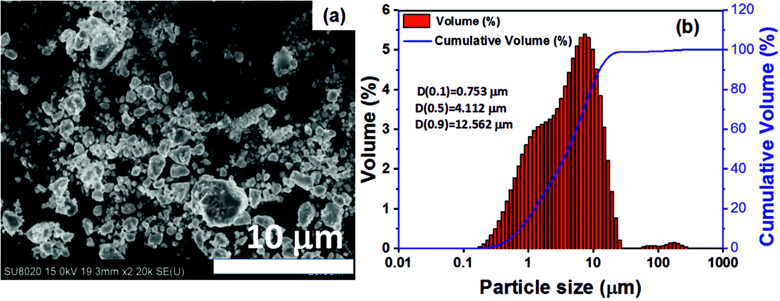 | ||
| Fig. 1 (a) FESEM image of the powder prepared by the SHS method; (b) particle size distribution for the same powder as (a). | ||
3. Results and discussions
3.1 Processing window
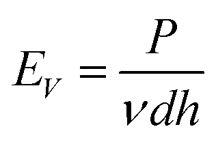
Fig. 2 shows the influence of the SLM processing parameters on the quality of a single forming layer. We use the laser volume energy density EV,33 defined as
 | (1) |
 | ||
| Fig. 2 FESEM images show four typical surface morphologies of SLM-prepared ZrNiSn single layers: (a) overheated; (b) distorted; (c) flat; (d) balling. (e) The processing window with varying laser powers and scanning speeds delineates the above four types of layer finish during SLM. | ||
The processing parameters corresponding to the above four typical morphologies are as follows: the overheated forming area in Fig. 2(a) is a result of using too high laser power (P > 22 W) and low scanning speeds (ν ≤ 80 mm s−1). This corresponds to the laser volume energy density of EV ≥ 220 J mm−3, in which case the boundary region between the processed and unprocessed layer of powder develops a distinct concave profile. The molten pool temperature under such high EV is so high that the surrounding un-scanned powder is also partially melted. Moreover, in such hot molten pool, chemical elements readily evaporate.
Fig. 2(b) depicts the distorted forming area obtained under high laser power (P > 22 W) but a somewhat increased scanning speeds (80 ≤ ν ≤ 120 mm s−1). The laser energy density is then within the range 146 J mm−3 < EV < 220 J mm−3, and the concave profile has disappeared. However, significant layer thickness fluctuations were observed between the boundaries and the middle region. They originate from the actual scanning speed at the start and end points of the scanned track where the laser motion is much slower than the speed over the central region of the track. Accordingly, the laser beam interacts with the powder bed for a longer time at both ends of the track, the temperature of the molten pool there increases, giving rise to raised edges at both ends.
In Fig. 2(c), flat area is obtained under the laser power within the range 14 W < P ≤ 20 W and scanning speeds between 80 mm s−1 and 120 mm s−1. In terms of the laser energy density EV this is an interval between 88 J mm−3 and 146 J mm−3. Operating under these conditions results in no ridge-like features on the surface.
In Fig. 2(d), one observes distinct balling, which reflects a low laser power (P ≤ 14 W) and/or high scanning speed (ν > 120 mm s−1), corresponding to the energy density of EV < 88 J mm−3. The laser energy is not high enough to melt the powder bed completely. Consequently, the molten pool is shallow, its temperature is too low and the viscosity of the melt is large. Such conditions lead to a large wetting angle that readily produces the balling phenomenon.
According to the above results, provided the laser power and the scanning speed are controlled between 14 W to 20 W and 80 mm s−1 to 120 mm s−1, respectively (EV between 88 J mm−3 to 146 J mm−3), flat high quality surfaces form. Though the hatch spacing (h) and the thickness of the powder bed (d) play an important role in determining the quality of the forming layer, the main governing factors are the laser power and the scanning speed.
3.2 Chemical composition
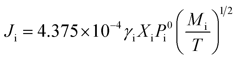
Chemical composition is the key factor determining material properties, especially as far as the thermoelectric materials are concerned. Since the ZrNiSn alloy consists of high and low melting point elements and the molten pool reaches rather high temperatures, accelerated evaporation of some elements is a concern that must be addressed during the SLM processing.The vapor pressure Pi (Pa) and the vaporization rate Ji (g cm−2 s−1) of element i, calculated according to the Langmuir formula, are introduced to analyze variations in the content of elements constituting ZrNiSn during SLM.
The vapor pressure Pi can be expressed as:34
 | (2) |
 | (3) |
After calculating the vapor pressure Pi, we substitute eqn (2) into eqn (3) to obtain the vaporization rate Ji of the elements Zr, Ni, Sn, respectively. Fig. 3(a) shows the temperature dependence of the evaporation rates of Zr, Ni, Sn from 1200 K to 3000 K. The vaporization rates of Zr and Ni are low during in the whole temperature range, while Sn evaporates at an increasing rate as the temperature increases and its loss is greater than that of Ni and particularly so compared to Zr.
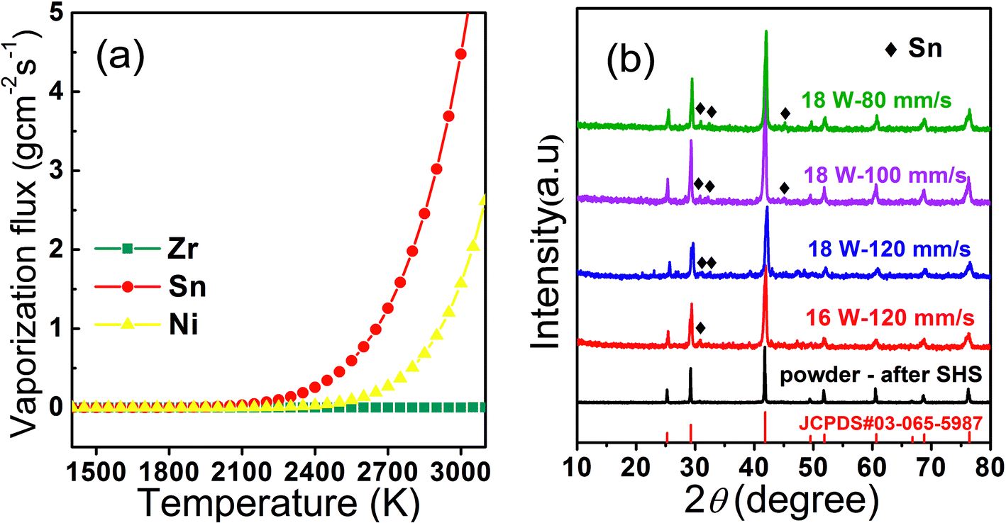 | ||
| Fig. 3 (a) Calculated vaporization rates of Zr, Ni, Sn as a function of the molten pool temperature; (b) X-ray diffraction patterns of SLM-processed layers with flat surface under varying laser powers and scanning speeds. The reference pattern (JCPDS#03-065-5987) for ZrNiSn is also shown for comparison. | ||
Fig. 3(b) shows the XRD patterns of four well-formed surfaces prepared using the following laser parameters: 16 W and 120 mm s−1; 18 W and 120 mm s−1; 18 W and 100 mm s−1; and 18 W and 80 mm s−1, respectively. All patterns indicate the same main phase of ZrNiSn and a secondary phase of Sn. The observation of Sn as a second phase could be correlated to the possible phase segregation from half-heusler ZrNiSn to full Heusler ZrNi2Sn, Sn and Zr. However, Zr exist in the form of ZrO2, which could be seen from the SEM photo given in Fig. S1.† On the other hand, the loss of Sn in ZrNiSn will result in Sn vacancy and Zr/Sn antisite defects. As the laser power increases and the scanning speed decreases, the depth of the molten pool increases and the bonding between the layers becomes stronger. Consequently, we have chosen to operate with the laser parameters of P = 18 W, ν = 80 mm s−1, h = 50 μm, and d = 30 μm.
Fig. 4 depicts the shape, morphology, and the phase composition of the 1.7 mm thick SLM-processed ZrNiSn. The actual composition of SLM-processed ZrNiSn (ZrNi1.009Sn1.018) before annealing is close to that of the SPS-processed ZrNiSn (ZrNi1.003Sn1.016). After annealing, the actual composition of the SHS-SLM sample kept almost unchanged (ZrNi1.010Sn1.020). Fig. 4(a) shows that the surface of the processed structure is relatively flat. The side view of the structure is shown in Fig. 4(b). The images document that ZrNiSn can be successfully printed on the Ti substrate. Fig. 4(c) is the surface FESEM image of ZrNiSn. A few cracks are visible under high magnification. Fig. 4(d) is the FESEM image of the cross section of the SLM-processed ZrNiSn. The white arrow denotes the direction of the building layers and the red dotted line indicates the boundary between the bulk and the Ti substrate. There are a few cracks paralleled to the building direction observed on the cross section in Fig. 4(d). These cracks arise from a very rapid rate of cooling that can reach values on the order of 106 K s−1. Fig. 4(e)–(h) present cross-section images of the element maps at the interface between ZrNiSn and the Ti substrate. The interface is smooth and sharp and no inter-diffusion is observed. It follows that ZrNiSn can be printed on the Ti substrate without a transition layer due to comparable melting points and thermal expansion coefficients. Therefore, ZrNiSn legs can be prepared in one step by SLM.
 | ||
| Fig. 4 (a) Images of the SLM-processed ZrNiSn on the Ti substrate (top view); (b) side view of the structure; (c) SEM image of the surface of SLM-processed ZrNiSn; (d) SEM image showing the interface between ZrNiSn and Ti highlighted by the red dashed line; (e)–(h) EDS elemental maps of the green rectangular area in (d). | ||
3.3 Thermoelectric transport properties
The bulk ZrNiSn sample with the thickness of 1.7 mm, representing 80 individual processed layers on top of each other, was prepared with the relative density of 97.2%. Fig. 5 shows thermoelectric transport properties of the structure. Temperature dependence of the electrical conductivity is shown in Fig. 5(a) and includes, for comparison, the conductivity of the SHS-SLM-processed sample annealed at 500 °C for 24 hours and the SHS-SPS-processed sample. As the temperature increases, the electrical conductivity of the as-prepared SHS-SLM sample initially slowly increases. Above about 475 K, the rate of increase accelerates until near 750 K, at which point the conductivity flattens. Up to 650 K, the conductivity of the SHS-SLM sample is significantly inferior to the conductivity of the SHS-SPS sample, in spite of its carrier concentration (7.54 × 1020 cm−3 at room temperature) being more than an order of magnitude larger than the carrier concentration (5.87 × 1019 cm−3 at room temperature) in the SHS-SPS sample. Therefore, SLM-processed samples must have much lower carrier mobility compared with the SPS'ed samples. This is mainly due to the microcrack formed in the SLM-process sample. We have attempted to improve the electrical conductivity by annealing the SHS-SLM sample and, indeed, this led to a marked improvement. Apparently, upon annealing, some of the cracks have been eliminated. It is noted that the conductivity of SHS-SLM prepared sample actually increase with the elevated temperature. This could be explained by the band gap shrinkage36 due to the existence of the Zr/Sn antisite defect. Due to the band gap shrinkage, the SLM sample experiences the minor carrier excitation even at a much higher carrier concentration as compared with the SPS prepared sample. Fig. 5(b) shows the Seebeck coefficient of all three specimens. Obviously, the Seebeck coefficient of the SHS-SLM sample is lower than that of the SHS-SPS sample, which can be ascribed to its much higher carrier concentration. Due to the much lower Seebeck coefficient and comparable electrical conductivities, the power factor of the SHS-SLM-processed ZrNiSn (1.45 mW m−1 K−2 at 873 K) is significantly smaller than the power factor of the SHS-SPS-prepared sample (3.4 mW m−1 K−2 at 873 K). Fig. 5(c) shows the thermal conductivity of the three samples. The thermal conductivity of the SHS-SLM-processed ZrNiSn is significantly lower than the thermal conductivity of the SHS-SPS-prepared ZrNiSn. For example, at 873 K, the respective thermal conductivities are 3.83 W m−1 K−1 and 4.96 W m−1 K−1. Beside the presence of micro-cracks, the significantly decreased thermal conductivity of the SHS-SLM-processed ZrNiSn is chiefly due to the extremely fast heating and cooling rates during SLM, which result in fine submicron-size grain structure. Annealing has no effect on the magnitude of the thermal conductivity of SHS-SLM sample. Fig. 5(d) shows the temperature dependence of ZT values of all three samples. Compared to the SHS-SPS sample, the SHS-SLM structure attains only about 59% the value of ZT, and at 873 K it reaches 0.39 versus 0.66. The difference in ZT values is attributed to an order of magnitude larger carrier concentration in SHS-SLM-processed ZrNiSn that primarily affects the magnitude of the Seebeck coefficient.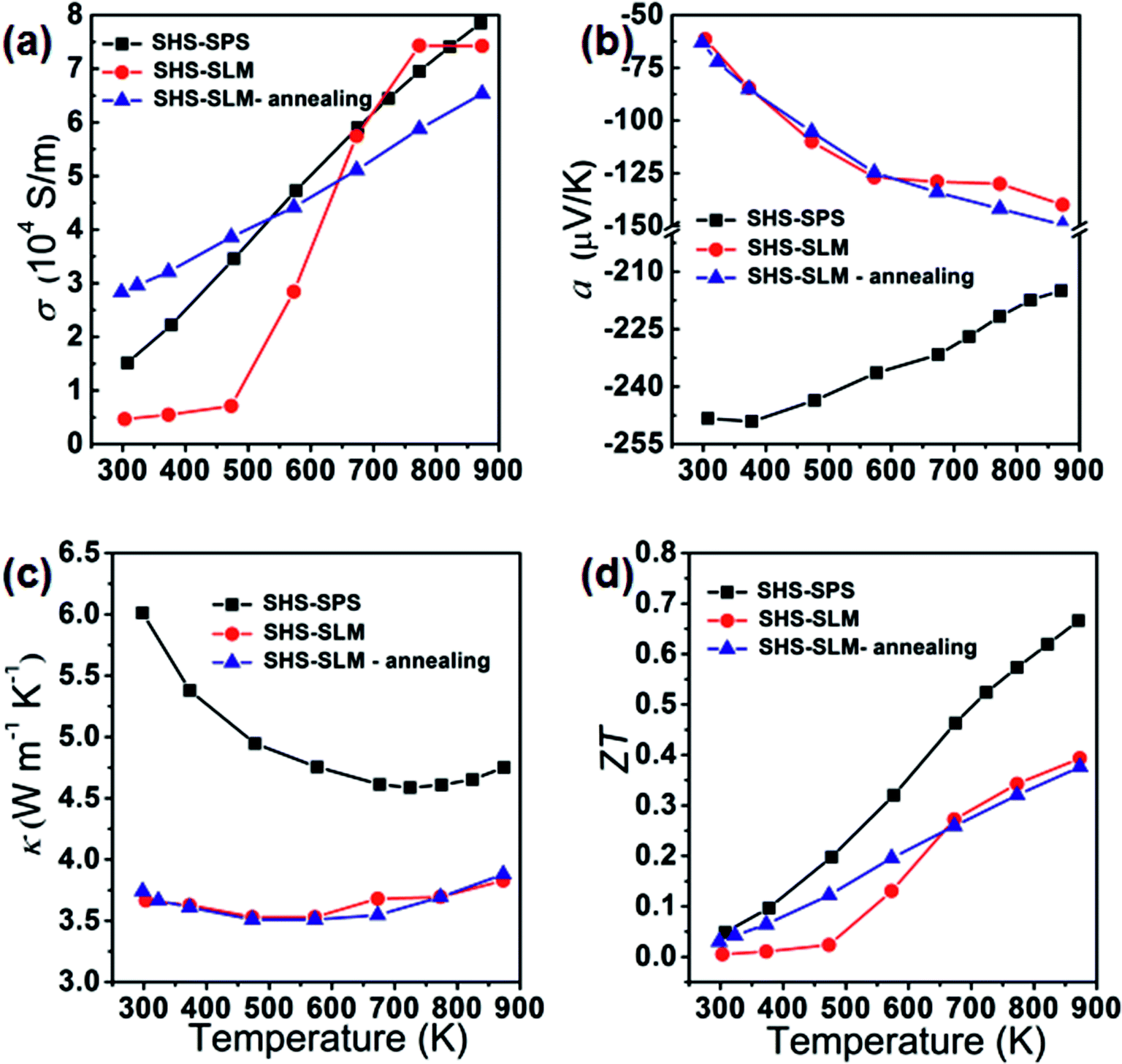 | ||
| Fig. 5 Temperature dependence of thermoelectric properties of SLM-processed ZrNiSn (before and after annealing) compared to ZrNiSn prepared by SHS-SPS: (a) electrical conductivity; (b) Seebeck coefficient; (c) thermal conductivity; and (d) thermoelectric figure of merit ZT. The SHS-SLM sample was annealed at 500 °C for 24 hours. | ||
Fig. 6 presents cross-section FESEM images of SHS-SPS and SHS-SLM prepared ZrNiSn. Fig. 6(a) shows the grain size of a few μm, typical of the SHS-SPS-processed structure. In Fig. 6(b) is shown a submicron grain structure formed during the SHS-SLM processing of ZrNiSn, where the cooling rate is so fast (more than 106 K s−1) that the grain growth is seriously impeded. This fine microstructure should enhance scattering of phonons and result in significantly reduced thermal conductivity, as is indeed, observed.
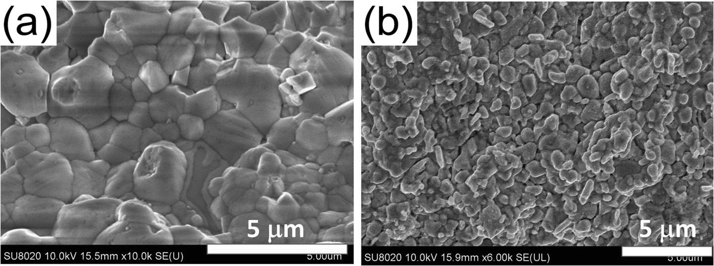 | ||
| Fig. 6 FESEM images of the cross-section of ZrNiSn samples: (a) SHS-SPS-prepared sample; (b) SHS-SLM-processed sample. Note the grain size difference. | ||
The joining of ZrNiSn and metal substrate can be considered as laser welding. Only when the two materials have similar melting points and coefficients of thermal expansion, can they form a suitable bonding. By a survey on common metals, Ti shows a close melting point and a similar thermal expansion coefficient to ZrNiSn. Therefore, we select Ti as the proper electrode for ZrNiSn to ensure good bonding. Fig. 7(a) and (b) shows backscattering electron image of the interface of SLM-processed ZrNiSn on Ti substrate before and after annealing, respectively. After annealing, the interphase layer thickness does not change and are around 5 μm, this region possesses a Ti-rich composition, formed due to the inter-diffusion between Ti and ZrNiSn during the SLM process. After annealing, a slight diffusion of Ti into ZrNiSn can be observed. Fig. 7(c) shows the contact resistance between the Ti substrate and the SHS-SLM-processed ZrNiSn after annealing which is measured as 0.436 mΩ. This corresponds to the contact resistivity of 27.25 μΩ cm2, which is a comparable value with those observed on the interfaces of the commercial TE modules.37 The interfacial region attributes to the contact resistivity and also assures a good bonding strength between ZrNiSn and Ti.
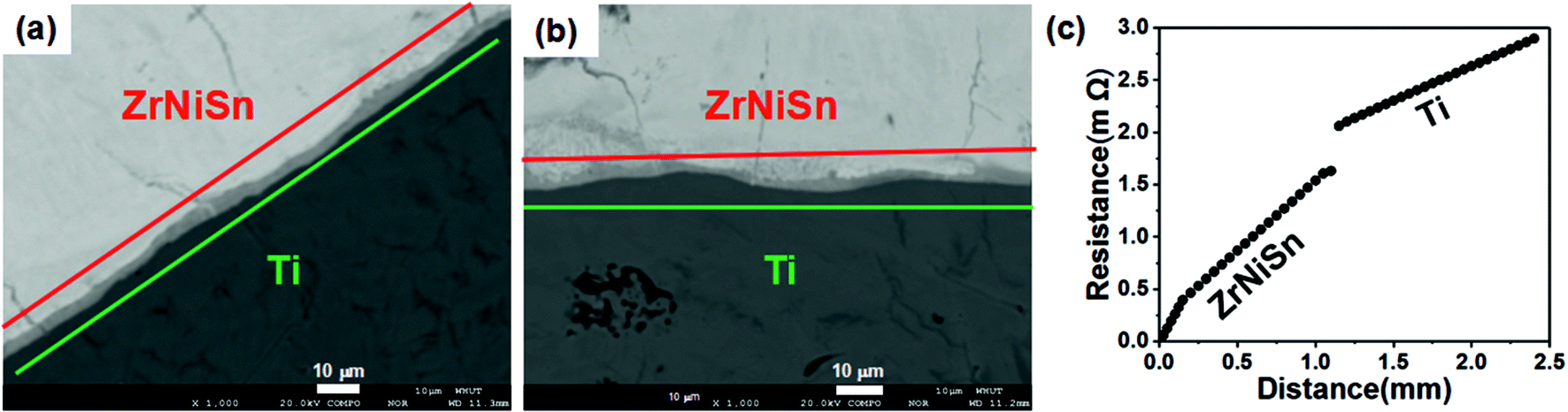 | ||
| Fig. 7 Backscattering electron image of the interface of the SLM-processed ZrNiSn on Ti substrate: (a) before and (b) after annealing; (c) contact resistance between the Ti substrate and the annealed SHS-SLM-processed ZrNiSn. | ||
4. Conclusions
We have explored a rapid, non-equilibrium SLM-based fabrication process of ZrNiSn, one of the promising novel thermoelectric materials. Results show that the laser energy density has the dominant influence on the material's forming quality, stoichiometry, phase composition and thermoelectric properties. The optimal laser energy density for obtaining excellent surface quality and a near theoretical density is in the range of 88 J mm−3 to 146 J mm−3. Deviating from this range results in porous, distorted and even balling surface. During the SLM processing of ZrNiSn, a small amount of Sn has appeared as a secondary phase. The presence of the Sn secondary phase has resulted in a large charge carrier concentration, an order of magnitude exceeding the carrier density of ZrNiSn prepared by SHS-SPS. Due to such greatly enhanced carrier concentration, the Seebeck coefficient of the SHS-SLM-processed ZrNiSn is significantly inferior to that of the SHS-SPS-processed material, and this is reflected in only about 59% the value of ZT (0.39 at 873 K) obtained for this SLM-based structure.It is the first time that ZrNiSn was printed on the Ti substrate, realizing a one-step preparation of ZrNiSn thermoelectric legs. This lays an important foundation for subsequent efforts to manufacture ZrNiSn-based modules by SLM and extending the technology to other thermoelectric materials.
Conflicts of interest
There are no conflicts to declare.Acknowledgements
We wish to acknowledge support from the Natural Science Foundation of China (Grant No. 51521001, 51401153, 517772232) and the 111 Project of China (Grant No. B07040).References
- T. M. Tritt and M. A. Subramanian, MRS Bull., 2006, 31, 188–195 CrossRef.
- Y. Zhang, M. Cleary, X. Wang, N. Kempf, L. Schoensee, J. Yang, G. Joshi and L. Meda, Energy Convers. Manage., 2015, 105, 946–950 CrossRef.
- Q. H. Zhang, X. Y. Huang, S. Q. Bai, X. Shi, C. Uher and L. D. Chen, Adv. Eng. Mater., 2016, 18, 194–213 CrossRef CAS.
- J. H. Yang and T. Caillat, MRS Bull., 2006, 31, 224–229 CrossRef CAS.
- J. Schmitt, Z. M. Gibbs, G. J. Snyder and C. Felser, Mater. Horiz., 2015, 2, 68–75 RSC.
- H. Xie, H. Wang, C. Fu, Y. Liu, G. J. Snyder, X. Zhao and T. Zhu, Sci. Rep., 2014, 4, 6888 CrossRef CAS PubMed.
- G. Rogl, A. Grytsiv, M. Gürth, A. Tavassoli, C. Ebner, A. Wünschek, S. Puchegger, V. Soprunyuk, W. Schranz, H. EuMuller, M. Zehetbauer and P. Rogl, Acta Mater., 2016, 107, 178–195 CrossRef CAS.
- S. Populoh, O. Brunko, K. Gałązka, W. Xie and A. Weidenkaff, Materials, 2013, 6, 1326–1332 CrossRef CAS PubMed.
- S. Sakurada and N. Shutoh, Appl. Phys. Lett., 2005, 86, 3159 CrossRef.
- P. Qiu, J. Yang, X. Huang, X. Chen and L. Chen, Appl. Phys. Lett., 2010, 96, 3159 Search PubMed.
- W. J. Xie, Y. G. Yan, S. Zhu, M. Zhou, S. Populoh, K. Galazka, S. J. Poon, A. Weidenkaff, J. He, X. F. Tang and T. M. Tritt, Acta Mater., 2013, 61, 2087–2094 CrossRef CAS.
- C. Fu, S. Bai, Y. Liu, Y. Tang, L. Chen, X. Zhao and T. Zhu, Nat. Commun., 2015, 6, 8144 CrossRef PubMed.
- J. P. A. Makongo, D. K. Misra, J. R. Salvador, N. J. Takas, G. Y. Wang, M. R. Shabetai, A. Pant, P. Paudel, C. Uher, K. L. Stokes and P. F. P. Poudeu, J. Solid State Chem., 2011, 184, 2948–2960 CrossRef CAS.
- J. P. Makongo, D. K. Misra, X. Y. Zhou, A. Pant, M. R. Shabetai, X. L. Su, C. Uher, K. L. Stokes and P. P. F. Poudeu, J. Am. Chem. Soc., 2011, 133, 18843 CrossRef CAS PubMed.
- S. Y. Wang, G. J. Tan, W. J. Xie, G. Zheng, H. Li, J. H. Yang and X. F. Tang, J. Mater. Chem., 2013, 10, 20130070 Search PubMed.
- L. E. Bell, Science, 2008, 321, 1457–1461 CrossRef CAS PubMed.
- L. D. Zhao, B. P. Zhang, J. Li, H. Zhang and W. Liu, Solid State Sci., 2008, 10, 651–658 CrossRef CAS.
- A. Merzhanov, Ceram. Int., 1995, 21, 371–379 CrossRef CAS.
- J. Subrahmanyam and M. Vijayakumar, J. Mater. Sci., 1992, 27, 6249–6273 CrossRef CAS.
- A. G. Merzhanov, Adv. Mater., 1990, 2, 314–316 CrossRef.
- X. L. Su, F. Fu, Y. G. Yan, G. Zheng, T. Liang, Q. Zhang, X. Cheng, D. W. Yang, H. Chi, X. F. Tang, Q. J. Zhang and C. Uher, Nat. Commun., 2014, 5, 4908 CrossRef CAS PubMed.
- G. Zheng, X. L. Su, X. Li, T. Liang, H. Y. Xie, X. Y. She, Y. G. Yan, C. Uher, M. G. Kanatzidis and X. F. Tang, Adv. Energy Mater., 2016, 6, 1600595 CrossRef.
- G. Zheng, X. L. Su, T. Liang, Q. B. Lu, Y. G. Yan, C. Uher and X. F. Tang, J. Mater. Chem. A, 2015, 3, 6603–6613 CAS.
- T. Liang, X. L. Su, Y. G. Yan, G. Zheng, Q. Zhang, H. Chi, X. F. Tang and C. Uher, J. Mater. Chem. A, 2014, 2, 17914–17918 CAS.
- D. W. Yang, X. L. Su, Y. G. Yan, T. Z. Hu, H. Y. Xie, J. He, C. Uher, M. G. Kanatzidis and X. F. Tang, Chem. Mater., 2016, 28, 4628–4640 CrossRef CAS.
- T. Liang, X. L. Su, X. M. Tan, G. Zheng, X. Y. She, Y. G. Yan, X. F. Tang and C. Uher, J. Mater. Chem. C, 2015, 3, 8550–8558 RSC.
- T. Z. Hu, D. W. Yang, X. L. Su, Y. G. Yan, Y. H. You, W. Liu, C. Uher and X. F. Tang, ACS Appl. Mater. Interfaces, 2018, 10, 864–872 CAS.
- D. D. Gu, W. Meiners, K. Wissenbach and R. Poprawe, Int. Mater. Rev., 2017, 57, 133–164 CrossRef.
- J. D. Majumdar and I. Manna, Int. Mater. Rev., 2013, 17, 519 Search PubMed.
- A. El-Desouky, M. Carter, M. A. Andre, P. M. Bardet and S. LeBlanc, Mater. Lett., 2016, 185, 598–602 CrossRef CAS.
- Y. Mao, Y. G. Yan, K. P. Wu, H. Y. Xie, Z. K. Xiu, J. H. Yang, Q. J. Zhang, C. Uher and X. F. Tang, RSC Adv., 2017, 7, 21439–21445 RSC.
- K. P. Wu, Y. G. Yan, J. Zhang, Y. Mao, H. Y. Xie, J. H. Yang, Q. J. Zhang, C. Uher and X. F. Tang, Phys. Status Solidi RRL, 2017, 11, 1700067 CrossRef.
- D. Wang, C. Song, Y. Yang and Y. Bai, Mater. Des., 2016, 100, 291–299 CrossRef CAS.
- A. Block-Bolten and T. W. Eagar, Metall. Mater. Trans. B, 1984, 15, 461–469 CrossRef.
- E. Brandes and G. Brook, Smithells Metals Reference Book, Elsevier Butterworth-Heinemann, Oxford and Boston, 1998 Search PubMed.
- P. F. Qiu, J. Yang, X. Y. Huang, X. H. Chen and L. D. Chen, Appl. Phys. Lett., 2010, 96, 3159 Search PubMed.
- D. J. Zhao, X. Y. Li, L. He, W. jiang and L. D. Chen, Intermetallics, 2009, 17, 136–141 CrossRef CAS.
Footnote |
| † Electronic supplementary information (ESI) available. See DOI: 10.1039/c8ra00992a |
| This journal is © The Royal Society of Chemistry 2018 |