
 Open Access Article
 This Open Access Article is licensed under a Creative Commons Attribution-Non Commercial 3.0 Unported Licence
Growth promotion of vertical graphene on SiO2/Si by Ar plasma process in plasma-enhanced chemical vapor deposition†
Yanping Suiab,
Zhiying Chenab,
Yanhui Zhangab,
Shike Huabc,
Yijian Liangabc,
Xiaoming Geabc,
Jing Liabc,
Guanghui Yu *ab,
Songang Pengd,
Zhi Jind and
Xinyu Liud
*ab,
Songang Pengd,
Zhi Jind and
Xinyu Liud
aState Key Laboratory of Functional Materials for Informatics, Shanghai Institute of Microsystem and Information Technoloy (SIMIT), Chinese Academy of Sciences, 865 Changning Road, Shanghai 200050, China. E-mail: ghyu@mail.sim.ac.cn
bCAS Center for Excellence in Superconducting Electronics, 865 Changning Road, Shanghai 200050, China
cUniversity of Chinese Academy of Sciences, No. 19A Yuquan Road, Beijing 100049, China
dMicrowave Devices and Integrated Circuits Department, Institute of Microelectronics, Chinese Academy of Sciences, 100029 Beijing, China
First published on 22nd May 2018
Abstract
This study investigates the growth promotion of vertically oriented graphene in plasma-enhanced chemical vapor deposition through Ar plasma treatment. Combined with various substrate treatments, including hydrofluoric acid etching and oxidation after Ar plasma treatment, Ar plasma pretreatment promotes vertical growth through the microcavity on the rough substrate surface and the active growth sites. The microcavity affects the strain distribution and defects of as-deposited planar films, which benefit the transition of 2D deposition to 3D vertical growth. A growth model on the effect of Ar plasma pretreatment is proposed.
Introduction
Plasma-enhanced chemical vapor deposition (PECVD) has emerged as an important method for producing carbon materials, such as diamonds, carbon nanotubes, vertically oriented graphene (VG) nanosheets, and graphene, on arbitrary substrates. The excitation and dissociation of hydrocarbon precursors are achieved by inelastic collisions with the electrons that carry high energy in the plasma, which is prone to form free radicals, ions, and other reactive species. Some studies have reported that graphene without transition metal catalyst should be grown under high temperature, highly dilutive hydrocarbon/carrier gas, and long growth time. In specific, high temperatures in the range of 1100 °C to 1650 °C and growth period up to several hours are needed.1,2 Thermal chemical vapor deposition is an appropriate approach for the synthesis of high-quality graphene (monolayer or few layers) on transition metal substrates. Thus, VG nanosheets are more preferably generated than monolayer graphene in PECVD. PECVD is performed at low temperatures without the use of catalysts. It has good control in nanostructure ordering and high purity, which can easily produce highly dense graphene nanosheets.3 Vertically oriented graphene nanosheets are presented as networks of “graphitic” platelets that are typically vertically oriented on a substrate; these nanosheets feature exposed sharp edges, non-stacking morphology, and a large surface-to-volume ratio. VG and its derivatives have many applications, such as in gas sensors and biosensors,4–6 field emission devices,7,8 and energy storage devices, such as supercapacitors, lithium-ion batteries, and fuel cells.9–14PECVD has attracted increasing attention as a promising method for controllable graphene synthesis. The substrate surface for carbon film growth is usually pretreated to ensure high nucleation density, decrease nucleation time, and improve adhesion. Various pretreatment methods, such as chemical and mechanical approaches, may be used.15,16 It is reported substrates were scratched by a diamond powder before deposition to create many surface defects and improve adhesion.15 Ar plasma sputtering is a comparatively common substrate treatment for film growth, but it is rarely mentioned in VG growth by PECVD. Few studies investigated the effect of Ar plasma treatment on the growth of vertically oriented graphene. The results of the present study showed that the growth of VG nanosheets is promoted by the convenient in situ substrate-pretreatment in PECVD. The effect of Ar plasma on the promotion of VG growth was studied.
Experimental
The samples employed in this study were fabricated by a radio frequency (RF)-PECVD system. The plasma was ignited using argon or a mixture blended with methane at an RF power of 350 W. The temperature of the sample stage ranged from 750 °C to 700 °C at a growth pressure of approximately 450 mTorr. Substrates first endured ultrasonic cleaning with organic cleaning liquid. The substrates were then treated by different processes for various samples before growth, such as dipping in hydrofluoric acid (HF), Ar plasma treatment (Arp), and oxidation after Ar plasma treatment (Arp + oxidation). HF etching was applied by dipping the substrate into diluted hydrofluoric acid (HF![[thin space (1/6-em)]](https://www.rsc.org/images/entities/char_2009.gif) :H2O = 1:20) for 10 s then rinsing it with deionized water. The Arp process was performed with pure argon, which was ignited for 20 min before the growth of VG nanosheets. Oxidation was carried out by introducing a mixture of oxygen and argon at 750 °C for 10 min after the Arp process. All samples were grown with the gas mixture flow rate Ar (100 sccm) and CH4 (2 sccm) at 700 °C. Approximately 300 nm of thermally grown SiO2 on a Si wafer was used as the substrate for our samples. The sample was immersed in diluted hydrofluoric acid, the VG nanosheets film was separated from the substrate and transferred with a micro grid for the preparation of TEM.
:H2O = 1:20) for 10 s then rinsing it with deionized water. The Arp process was performed with pure argon, which was ignited for 20 min before the growth of VG nanosheets. Oxidation was carried out by introducing a mixture of oxygen and argon at 750 °C for 10 min after the Arp process. All samples were grown with the gas mixture flow rate Ar (100 sccm) and CH4 (2 sccm) at 700 °C. Approximately 300 nm of thermally grown SiO2 on a Si wafer was used as the substrate for our samples. The sample was immersed in diluted hydrofluoric acid, the VG nanosheets film was separated from the substrate and transferred with a micro grid for the preparation of TEM.
The detailed investigation was based on scanning electron microscopy (SEM, Zeiss Supra55), atom force microscopy (AFM, Bruker Dimension Icon), Field Emission Transmission Electron Microscope (FE-TEM, JEM-2100F), thermo scientific DXR Raman spectroscopy with a 532 nm Nd:YAG laser, and X-ray photoelectron spectroscopy (XPS, Thermo Scientific ESCALAB 250).
Results and discussion
Fig. 1a–d indicate the surface morphologies and cross-sectional SEM images of VGNs grown on the substrates without pretreatment. After 5 min, the nanoflakes fail to completely cover the substrate, and vertically oriented graphene is absent (Fig. 1a). After 30 min, the growth of VG nanosheets remains sparse (Fig. 1b). However, Fig. 1e–h show the typical surface topography of VG nanosheets after growth on the substrates pretreated by Ar plasma. VG nanosheets with many vertical carbon edges are found even after 5 min of growth (Fig. 1e). The cross-sectional SEM images demonstrate that the graphene sheets are nearly perpendicular to the substrate and are thin and transparent. The height of the vertical sheets is approximately 130 nm after 5 min (Fig. 1g) and 150 nm after 30 min of growth (Fig. 1h). These results indicate that Ar plasma pretreatment promotes the growth of VG in PECVD.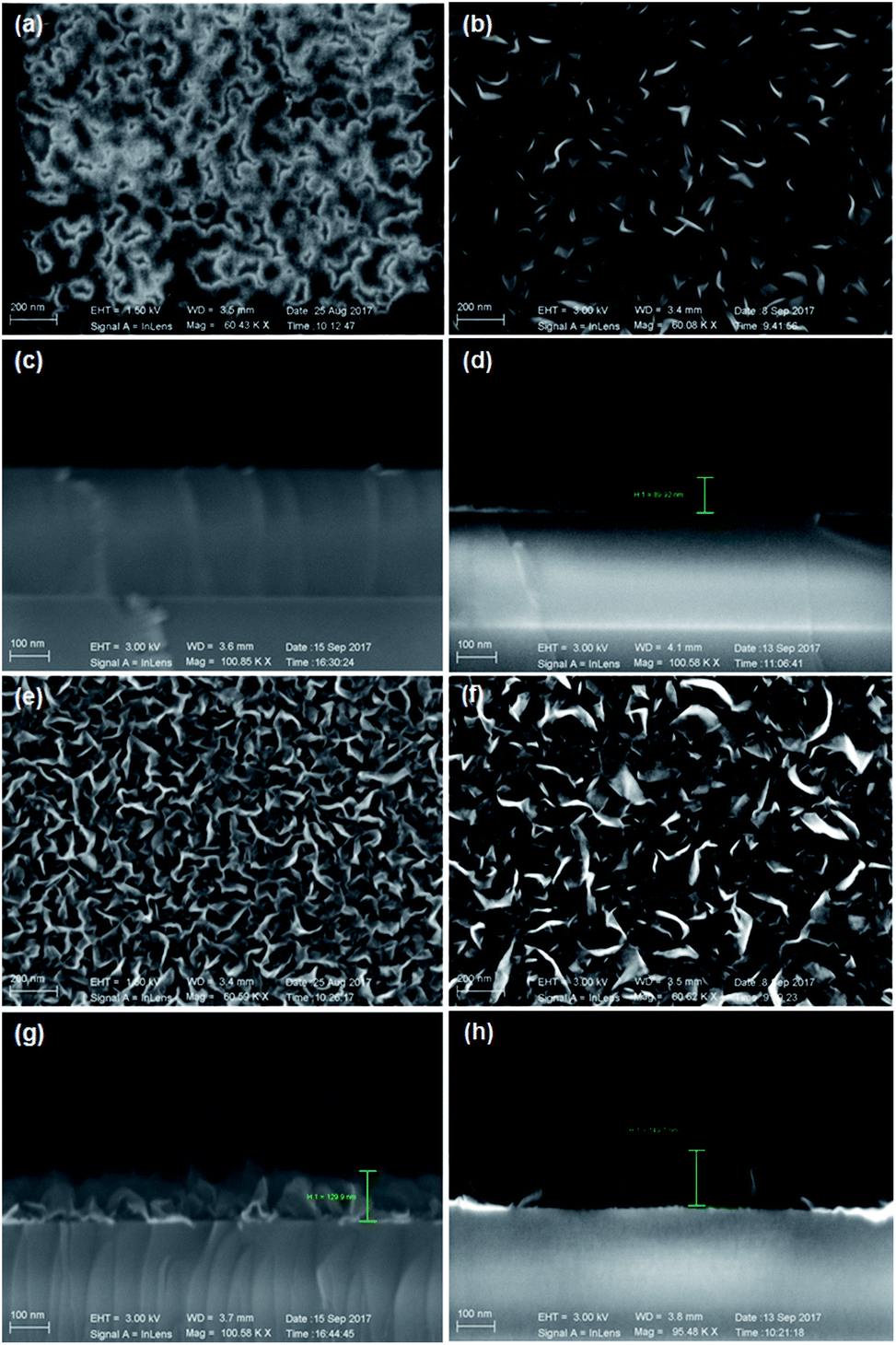 | ||
| Fig. 1 Top-view SEM images of VG deposited on untreated substrates for (a) 5 min and (b) 30 min; cross-sectional SEM images of VG on untreated substrates for (c) 5 min and (d) 30 min; top-view SEM of VG on Arp-treated substrates for (e) 5 min and (f) 30 min; cross-sectional SEM of VG on Arp-treated substrates for (g) 5 min and (h) 30 min. | ||
Fig. 2 indicate the top-view TEM images of VG with growth for 30 min on the Arp substrate shown in Fig. 1f and h. Fig. 2a exhibits the low-magnification TEM image of transparent VG film on micro grid. There is a lot of folds shown in Fig. 2b, which originate from that the vertical graphene nanosheets were bended into horizontal sheets in transferring process. Fig. 2c indicates the vertical graphene nanosheets consist of four layers up to more than ten parallel layers of graphene sheets.
 | ||
| Fig. 2 TEM images of VG with different magnification for (a)–(c). | ||
The effect of Ar plasma treatment on the subsequent VG growth can be attributed to the improvement of substrate, which promotes high nucleation density and improves adhesion. As the consequence of Ar plasma treatment, the substrates are changed in the roughness and active sites. The surface roughness of the substrates was tested by AFM. Another substrate dipped in diluted HF acid was tested for comparison purposes. Fig. 3a–c show the AFM images of the substrates treated by Ar plasma, HF dipping, and non-treatment, respectively. The roughness of the substrate treated by Ar plasma is ∼8.23 nm, which is larger than those of the two other substrates. The roughness of the HF-dipping-treated substrate is minimum. Fig. 3d and e show that VG grown on the HF-treated substrate for 5 min is sporadic and the planar nanoflakes nearly cover the substrate. Comparison of Fig. 1a and c indicates that VG growth on the HF-treated substrate is faster than that on the untreated substrate, although the roughness of the untreated substrate is larger than that of the HF-treated substrate. Therefore, except the factor of roughness, the active growth sites inspired by HF dipping promote VG growth. The Raman spectra of the VG grown on different substrates for 5 min are illustrated in Fig. 3f. The spectra of all substrates have three characteristic peaks that correspond to the D, G, and 2D bands, which reflect the features of the nanographene structure. The G band at ∼1583 cm−1 is an evidence of the carbon sp2 structure.17,18 The D band at ∼1348 cm−1 is attributed to the scattering at the defects or edges of the nanographene,19 and a shoulder D′ peak (∼1620 cm−1) at the right of the G band is also indicative of a defect or edge structure.20–22 It has been reported that the blueshift of the 2D peak compared with exfoliated graphene on SiO2 (2683 cm−1) agrees with the existence of compressive strain in planar few-layer graphene.23 Fig. 3f shows that the 2D-band blueshift of VG on Arp substrate is minimum (∼2690 cm−1), which indicates that the compressive strain in the sample is more fully released than that in other samples.
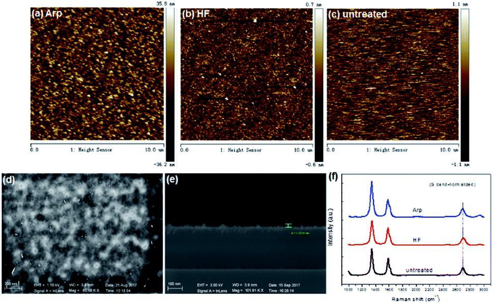 | ||
| Fig. 3 AFM images and height profiles (right) of substrates treated by (a) Arp, (b) HF, (c) untreated; (d) top-view and (e) cross-sectional SEM images of VG deposited on HF-dipping substrate for 5 min; and (f) Raman spectra of the VG grown on different substrates for 5 min. | ||
Another substrate was pretreated by Ar plasma and oxidation before growth to retain the same roughness as the substrate pretreated solely by Ar plasma. However, the active sites endured passivation to some extent. The VG growth for the initial 1 min on different substrates was compared (Fig. 4). The planar nanographene coverage of the substrate treated by Arp + oxidation is less than that treated solely by Arp. This result indicates that the reduction in active sites decreases carbon adhesion. VG growth for 30 min on the Arp + oxidation substrate (Fig. 4d and e) was compared with that in Fig. 1. The density and height of the VG nanosheets grown on the Arp + oxidation substrate are less than those of the nanosheets grown on the Arp substrate but are greater than those of the nanosheets grown on the untreated substrate. Fig. 4f exhibits that the intensity of the G band exceeds that of the D band with prolonged growth time. It means that the proportion of defects or nanosheet edges to the whole VG nanosheets is decreased, and the sp2 crystallite size of VG nanosheets is improved with growth time. In addition, comparing with the 2D peak position, the 2D-band blueshift of VG on Arp substrate is minimum, which indicates that the compressive strain in the sample is more fully released than that in the other samples. Moreover, the sheet resistance of graphene on the Arp substrate is ∼560 Ω □−1, which is smaller than that of the other samples.
 | ||
| Fig. 4 Top-view SEM images of VG grown for 1 min on (a) Arp, (b) untreated, (c) Arp + oxidation substrates, respectively; top-view SEM image (d) and cross-sectional SEM image (e) of VG grown for 30 min on Arp + oxidation; (f) Raman spectra of the VG grown on different substrates for 30 min. | ||
For the investigation of the early stages between VG and the variously treated substrates, the samples were grown for only 30 s on various substrates, and graphene/carbon deposition was invisible under a microscope. The XPS C1s spectra of the samples are shown in Fig. 5. The most intensive component is attributed to carbon in the sp2 and sp3 hybridization of C–C bonds (284.5 eV),24,25 which indicates that the carbon atom is deposited in the way of sp2 and sp3 hybridization state for the initial stage. For all samples, there is a decomposition peak at 285.9–286.4 eV which could be attributed to oxygen-related components, such as C–O groups.26 A differentiating component at ∼283.2 eV is present in the substrate-untreated sample (Fig. 5c), which agrees with the one of silicon carbide.27 At the surface of naturally oxidized silicon oxide, the silicon-to-oxygen ratio is not stoichiometric and has a low oxidation state.28 Thus, silicon excess at the surface of a substrate-untreated sample is more obvious than that of other samples given that the natural silicon oxide is etched by the treatment methods mentioned in this work, which is reflected in the component peak associated with silicon carbide. For the Arp + oxidation-treated sample, an additional weak component peak at ∼289.2 eV is ascribed to carbon in carboxylate groups,29 which means that oxygen is further absorbed on the surface after oxidation.
 | ||
| Fig. 5 C1s of X-ray photoelectron spectra for the nanographene grown for 30 s on the various substrates: (a) Ar plasma treated, (b) HF treated, (c) untreated, and (d) Ar plasma + oxidation treated. Black curves correspond to the experimental data. Blue curves show individual components as a result of the fitting procedure. | ||
Now the kinetic model of VG growth on the Ar plasma-treated substrate can be interpreted from two points of view: the roughness and active sites of the substrate. The schematic is shown in Fig. 6. For the untreated substrate, at the initial stage of growth, carbon precursors obtained from plasma are absorptive and form planar nanoflakes on the substrate. The absorptive carbon amount is small given the absence of active sites. The coverage of planar nanoflakes and the formation of VG nanosheets are slow on the untreated substrate. During the initial stage of growth, graphene layers grow parallel to the substrate surface until a sufficient level of force develops to curl the leading edge of the top layers upward. 20 The force that causes a transition from 2D planar films to 3D clusters could be ascribed to the strain and defect. First, after the planar graphene layers are deposited on the substrate, the intermediate layer causes a transition to 3D clusters beyond a critical layer thickness,30 because of the sufficient accumulation of strain energy in the system. This phenomenon follows the Stranski–Krastanov growth model.31 The results of the present work show that the strain in VG on the Ar plasma-treated substrates is less than that on the other samples, which indicates that the compressive strain could be more fully released by forming the dense VG nanosheets morphology in the Ar plasma-treated sample within the same growth time. The strain distribution on a smooth flat surface is different from that on the rough surface. In the microcavity of a rough surface (Fig. 3a), the adhesion of the carbon precursor is greater than on a flat surface. Thus, the strain in the graphene layers in the cavity increases fast to the extent of causing the top layers to move upward and causing the fast transition from 2D planar films to 3D clusters. Second, the nucleation and growth of the VGN are defect guided.32,33 In ion-assisted deposition, the precursors that possess high energy create defects on the film surface that could become new nucleation sites due to a high binding energy for growth.23 For the untreated substrate that is short of active growth sites, the defects of the as-deposited film are the main factor that leads to a vertical growth in the 3D clusters (Fig. 6a). However, for the Ar plasma-treated substrate with the microcavity during the deposition of the planar graphene layer, when the carbon precursors that extend horizontally meet the side wall of the cavity, the meeting sites may be similar to the defects for vertical growth (Fig. 6b). VG nanosheets growth is evidently promoted on the Ar plasma-treated substrate compared with the untreated substrate given a large amount of microcavity on the rough surface.
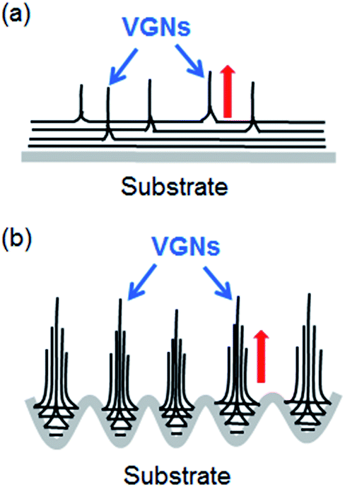 | ||
| Fig. 6 Scheme for the growth mechanism of the VGN on (a) untreated substrate and (b) Ar plasma treated substrate. The red arrows show the growth direction. | ||
The VG growth on the HF-treated substrate is faster than that on the untreated substrate, although the roughness of the HF-treated substrate is less than that of the untreated substrate (Fig. 3). The reason could be simply attributed to the active growth sites brought by HF etching of the substrate. Oxidation after the Ar plasma-treated substrate has the same roughness as the solely Ar plasma-treated substrate theoretically. The VG nanosheets grown on the former is not as dense as that on the latter, which is also because the active growth sites inspired by Ar plasma are partially passivated by the following oxidation.
To explore the application of VG grown in this work, electrochemical performance and contact angle measurement are presented in the ESI, which is shown in Fig. S1 and S2.†
Conclusions
This study investigated the growth promotion of vertically oriented graphene in PECVD by Ar plasma treatment through the characterizations of SEM, AFM, TEM, Raman, and XPS. Combined with the various treatments of the substrate, which includes HF etching and oxidation after Ar plasma treatment, the effect of Ar plasma treatment on the growth could be interpreted from the microcavity on the rough substrate surface and the active growth sites. The cavity affects the strain distribution and defects of as-deposited planar films, which benefits the transition of 2D deposition to 3D vertical growth. The active growth sites inspired by Ar plasma sputtering is another factor that promotes VG growth. A growth model has been described and proposes the effect of Ar plasma treatment.Conflicts of interest
There are no conflicts to declare.Acknowledgements
This work was supported by National Natural Science Foundation of China (No. 51402342), and the “Strategic Priority Research Program (B)” of the Chinese Academy of Sciences (Grant No. XDB04040300).References
- H. P. Wang, E. L. Gao, P. Liu, D. L. Zhou, D. C. Geng, X. D. Xue, L. P. Wang, K. L. Jiang, Z. P. Xu and G. Yu, Carbon, 2017, 121, 1–9 CrossRef.
- D. H. Liu, W. Yang, L. C. Zhang, J. Zhang, J. L. Meng, R. Yang, G. Y. Zhang and D. X. Shi, Carbon, 2014, 72, 387–392 CrossRef.
- M. L. Li, D. H. Liu, D. C. Wei, X. F. Song, D. P. Wei and A. T. S. Wee, Adv. Sci., 2016, 3, 1600003 CrossRef PubMed.
- K. Yu, Z. Bo, G. Lu, S. Mao, S. Cui, Y. Zhu, X. Chen, R. S. Ruoff and J. Chen, Nanoscale Res. Lett., 2011, 6, 202 CrossRef PubMed.
- N. G. Shang, P. Papakonstantinou, M. McMullan, M. Chu, A. Stamboulis, A. Potenza, S. S. Dhesi and H. Marchetto, Adv. Funct. Mater., 2008, 18, 3506–3514 CrossRef.
- K. H. Yu, G. H. Lu, Z. Bo, S. Mao and J. H. Chen, J. Phys. Chem. Lett., 2011, 2, 1556–1562 CrossRef.
- N. Soin, S. Sinha Roy, S. Roy, K. S. Hazra, D. S. Misra, T. H. Lim, C. J. Hetherington and J. A. McLaughlin, J. Phys. Chem. C, 2011, 115, 5366 Search PubMed.
- W. Takeuchi, H. Kondo, T. Obayashi, M. Hiramatsu and M. Hori, Appl. Phys. Lett., 2011, 98, 123107 CrossRef.
- M. Cai, R. A. Outlaw, S. M. Butler and J. R. Miller, Carbon, 2012, 50, 5481–5488 CrossRef.
- Z. Bo, Z. Wen, H. Kim, G. Lu, K. Yu and J. Chen, Carbon, 2012, 50, 4379–4387 CrossRef.
- H. Kim, Z. Wen, K. Yu, O. Mao and J. Chen, J. Mater. Chem., 2012, 22, 15514–15518 RSC.
- S. C. Shin, A. Yoshimura, T. Matsuo, M. Mori, M. Tanimura, A. Ishihara, K.-i. Ota and M. Tachibana, J. Appl. Phys., 2011, 110, 104308 CrossRef.
- N. Soin, S. S. Roy, T. H. Lim and J. A. D. McLaughlin, Mater. Chem. Phys., 2011, 129, 1051–1057 CrossRef.
- D. Wang, W. Zhang, N. E. Drewett, X. F. Liu, S. J. Yoo, S. G. Lee, J. G. Kim, T. Deng, X. Y. Zhang, X. Y. Shi and W. T. Zheng, ACS Cent. Sci., 2018, 4, 81–88 CrossRef PubMed.
- V. A. Krivchenko, A. A. Pilevsky, A. T. Rakhimov, B. V. Seleznev, N. V. Suetin, M. A. Timofeyev, A. V. Bespalov and O. L. Golikova, J. Appl. Phys., 2010, 107, 014315 CrossRef.
- D. Banerjee, S. Mukherjee and K. K. Chattopadhyay, Appl. Surf. Sci., 2011, 257, 3717–3722 CrossRef.
- A. C. Ferrari, J. C. Meyer, V. Scardaci, C. Casiraghi, M. Lazzeri, F. Mauri, S. Piscanec, D. Jiang, K. S. Novoselov, S. Roth and A. K. Geim, Phys. Rev. Lett., 2006, 97, 187401 CrossRef PubMed.
- W. Yang, G. Chen, Z. Shi, C. C. Liu, L. Zhang and G. Xie, Nat. Mater., 2013, 12, 792 CrossRef PubMed.
- A. C. Ferrari, Solid State Commun., 2007, 143, 47–57 CrossRef.
- M. S. Dresselhaus, A. Jorio, M. Hofmann, G. Dresselhaus and R. Saito, Nano Lett., 2010, 10, 751 CrossRef PubMed.
- D. C. Elias, R. R. Nair, T. M. G. Mohiuddin, S. V. Morozov, P. Blake and M. P. Halsall, Science, 2009, 323, 610 CrossRef PubMed.
- D. H. Liu, X. S. Chen, Y. B. Hu, T. Sun, Z. B. Song, Y. J. Zheng, Y. B. Cao, Z. Cai, M. Cao, L. Peng, Y. L. Huang, L. Du, W. L. Yang, G. Chen, D. P. Wei, A. T. S. Wee and D. C. Wei, Nat. Commun., 2018, 9, 193 CrossRef PubMed.
- L. L. Jiang, T. Z. Yang, F. Liu, J. Dong, Z. H. Yao, C. M. Shen, S. Z. Deng, N. S. Xu, Y. Q. Liu and H. J. Gao, Adv. Mater., 2013, 25, 250–255 CrossRef PubMed.
- E. Ech-chamikh, A. Essafti, Y. Ijdiyaou and M. Azizan, Sol. Energy Mater. Sol. Cells, 2006, 90, 1420–1423 CrossRef.
- S. Ghodbane, D. Ballutaud, F. Omnes and C. Agnes, Diamond Relat. Mater., 2010, 19, 630–636 CrossRef.
- S. K. Jerng, D. S. Yu, J. H. Lee, C. Kim, S. Yoon and S. H. Chun, Nanoscale Res. Lett., 2011, 6, 565 CrossRef PubMed.
- B. P. Swain, Surf. Coat. Technol., 2006, 201, 1589–1593 CrossRef.
- Y. Z. Wang, M. W. Chen, Y. M. Xie, P. R. Wei, H. F. Schaefer III, P. v. R. Schleyer and G. H. Robinson, Nat. Chem., 2015, 7, 509–513 CrossRef PubMed.
- G. Beamson and D. Briggs, High resolution XPS of organic polymers. The scienta ESCA300 Database, John Wiley & Sons, Chichester, 1992 Search PubMed.
- Z. Zhang, Science, 1997, 276, 377 CrossRef PubMed.
- J. A. Venables, G. D. T. Spiller and M. Hanbucken, Rep. Prog. Phys., 1984, 47, 399 CrossRef.
- J. H. Deng, R. T. Zheng, Y. Zhao and G. A. Cheng, ACS Nano, 2012, 6, 3727–3733 CrossRef PubMed.
- A. Malesevic, R. Vitchev, K. Schouteden, A. Volodin, L. Zhang, G. Van Tendeloo, A. Vanhulsel and C. V. Haesendonck, Nanotechnology, 2008, 19, 305604 CrossRef PubMed.
Footnote |
| † Electronic supplementary information (ESI) available. See DOI: 10.1039/c8ra00869h |
| This journal is © The Royal Society of Chemistry 2018 |