
 Open Access Article
 This Open Access Article is licensed under a Creative Commons Attribution-Non Commercial 3.0 Unported Licence
Polymer network hole transport layers based on photochemically cross-linkable N′N′-diallyl amide tri-N-substituted triazatruxene monomers†
Guang Hu a,
Stuart P. Kitney*b,
Stephen M. Kelly*a,
William Harrisonb,
Brian Lambertb and
Mary O'Neillc
a,
Stuart P. Kitney*b,
Stephen M. Kelly*a,
William Harrisonb,
Brian Lambertb and
Mary O'Neillc
aSchool of Mathematics and Physical Sciences, University of Hull, Cottingham Road, Hull, HU6 7RX, UK. E-mail: s.m.kelly@hull.ac.uk
bPolar OLED, University of Hull, Cottingham Road, Hull, HU6 7RX, UK. E-mail: stuart.kitney@npl.co.uk
cSchool of Science and Technology, Nottingham Trent University, Shakespeare Street, Nottingham, NG1 4FQ, UK
First published on 23rd February 2018
Abstract
Novel phtotpolymerisable hole-transport layers based on novel triazatruxenes incorporating six non-conjugated dienes as photo cross-linkable end-groups attached to flexible, aliphatic spacers have been synthesised using simple one-step substitution reactions. Hole-only test devices, fabricated using a combination of solution-deposition, spin-coating and initiator-free photochemical cross-linking of these photopolymerisable triazatruxenes, exhibit almost identical current density vs. voltage profiles before and after cross-linking, and as such, represent a promising new class of hole-transport layer for plastic electronic devices.
1 Introduction
Plastic electronics1–4 are replacing silicon for many consumer electronic applications, such as Organic Light-Emitting Diodes (OLEDs)5–8 and Organic Photovoltaics (OPVs),9–13 thereby creating new markets for novel electrooptic and electronic devices based on organic semiconductors. These optical–electrical devices usually require highly π-conjugated aromatic materials as organic semiconductors used as hole-transporting, electron-transporting or electroluminescent materials. In recent years, starburst triazatruxene materials with a disc-like, C3-symmetric structure and incorporating three carbazole units sharing an aromatic ring possessing an extended and highly conjugated π-system exhibit high hole-transport mobility and intense photo- and electro-luminescence for potential application in plastic electronic devices.14–17 The presence of three amino groups (–NH) facilitates the synthesis of a wide range of materials due to three facile points for the attachment of flexible aliphatic side chains that render the resulting materials soluble in common organic solvents used to deposit organic semiconductors from solution, such as spin coating, drop casting, doctor blade techniques, etc., on substrate surfaces as uniform thin films. The starburst structure of such triazatruxene derivatives prevents molecular close packing and spatial reorientation, thus suppressing self-aggregation and facilitating the formation of homogeneous, high-quality thin films on electrooptic and electronic device substrates.18 Derivatives incorporating the triazatruxene moiety have been the subject of limited interest as organic semiconductors, such as N-alkyl-substituted columnar liquid crystals and some oligomers, in plastic electronic devices.19–29 In contrast, a wide range of derivatives of the all-carbon counterpart truxene and thiatruxene has been extensively studied as organic semiconductors in electro optical or electrical devices.30–32Commercially available poly(3,4-ethylenedioxythiophene)polystyrene sulfonate (PEDOT:PSS) has been commonly used in OLEDs and Polymer Organic Light-Emitting Diodes (PLEDs) as an hole-injection layer, due to its intrinsically high conductivity (3.0 × 10⁻³ S cm−1)33 and ability to be deposited on a device substrate from solution. An additional hole-transport layer on top of the hole-injection layer is often used to control the current of holes and act as an electron-blocking layer and thereby to avoid unbalanced charge injection and charge mobility in multilayer OLEDs and PLEDs, for example, and thereby to achieve high efficiency of emission. In the absence of a hole-transport layer, charge recombination occurs predominantly near the cathode, which results in quenching of the excitons without light emission. The HOMO energy level of PEDOT:PSS is higher (−5.2 eV),33 than that of common emissive materials used in OLEDs and PLEDs (−5.5 eV or lower), which results in a mismatch of 0.3 eV or more. Therefore, in order to produce an insoluble hole-transport layer compatible with PEDOT:PSS and other hole-injection layers, two photopolymerisable carbazole-functionalised triazatruxene materials were synthesised in this work using simple N-substitution reactions of carbazole moieties. These triazatruxenes incorporate three photopolymerisable side-groups consisting of non-conjugated dienes34 at the end of aliphatic flexible spacers. These new photopolymerisable monomers can be deposited from solution, by spin casting or spin coating, as uniform thin layers on a device substrate with the desired thickness and then converted into the corresponding insoluble and intractable polymer networks as thin films for use as hole-transport layers in a range of multilayer organic semiconductor devices.
The advantages of using insoluble, intractable, and highly crosslinked polymer networks35–40 in multilayer plastic electronic devices include lower cost, scalability, i.e., the possibility to manufacture very large devices, and the use of standard fabrication equipment and processes in a continuous, rather than a batch, production process, e.g., the potential for continuous roll-to-roll production on plastic substrates. This approach facilitates pixelation, in OLEDs and PLEDs for example, using standard photolithography procedures in that unexposed and non-crosslinked regions can be easily removed by washing with the original spin-casting solvent.41 Unfortunately, the fluence of UV-illumination required during the photopolymerisation of the monomer in order to generate the corresponding polymer network with a sufficiently high crosslinking density to function as an insoluble thin solid layer often gives rise to a degree of photodegradation of the monomer and the polymer network as well as resulting in the formation of deep traps that can lead to values of the charge-carrier mobility of the polymer network that are several orders of magnitude lower than that of the monomer exposed to the UV-irradiation.41
2 Experimental
2.1 Synthesis of the photopolymerisable triazatruxenes 1 and 2
Triazatruxenes 1 and 2, Scheme 1, were synthesised by alkylation of the carbazole moieties present in triazatruxene using modified literature procedures.42,43 The reactions were carried out under a nitrogen atmosphere at 50 °C using a dispersion of sodium hydride as the base, N,N-dimethylformamide as the solvent and a 5.0 molar equivalent of N,N-diallyl-5-bromopentanamide or N,N-diallyl-2-bromoacetamide, respectively. The experimental procedures and NMR spectra are recorded in the ESI.† The cyclic voltammetry method used to measure the electrochemical energy levels of triazatruxenes 1 and 2 is described in the ESI† and the results displayed in Table 1.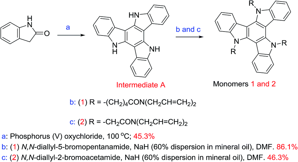 | ||
| Scheme 1 Triazatruxene 1 and 2 synthetic schemes, reaction conditions and yields. | ||
|
||||
|---|---|---|---|---|
| Monomer | R | IP (eV) | Eg (eV) | EA (eV) |
| 1 | –(CH2)4CON(CH2CH![[double bond, length as m-dash]](https://www.rsc.org/images/entities/char_e001.gif) CH2)2 CH2)2 |
5.35 | 3.39 | 1.96 |
| 2 | –CH2CON(CH2CHCH2)2 |
5.37 | 3.39 | 1.98 |
2.2 Photochemical crosslinking & UV-Vis absorption spectra
In order to study the effect of the UV-fluence on the degree of photochemically induced crosslinking, using UV-Vis absorption spectra, triazatruxenes 1 [R = –(CH2)4CON(CH2CHCH2)2] and 2 [R = –CH2CON(CH2CHCH2)2] were dissolved in chlorobenzene as 10 mg cm−3 solutions. These solutions were used to deposit a number of uniform thin films by spin-coating onto oxygen plasma-treated glass substrates at 2000 rpm and 2000 units acceleration. Seven films were subsequently exposed to different fluences of UV energy (365 nm), 1 @ 100 J cm−2 and 400 J cm−2; and 2 @ 0, 100 J cm−2, 200 J cm−2, 400 J cm−2, 600 J cm−2 and 800 J cm−2, and then annealed at 100 °C for 5 minutes. UV crosslinking was achieved using an OmniCure S2000 spot UV curing system. The measured fluence was calculated using the S2000 aperture and UV exposure timing settings, and calibrated using an OmniCure R2000 UV spot curing radiometer. The crosslink yield was determined as the difference in area under peak of the film before and after washing with chlorobenzene. Washing was achieved by placing each substrate on a spin coater, covering the substrate surface with chlorobenzene (1 cm3) and spinning the sample at 2000 rpm and 2000 units acceleration for 30 seconds.
2.3 Hole-only diode test devices
In order to measure the effect of UV-fluence – and by inference the degree of crosslinking and impact any photochemical degradation – on the magnitude of hole-transport mobility of the thin films of photopolymerised triazatruxenes, two hole-only test devices, see Fig. 1, were fabricated incorporating either the monomer 2 [R = –CH2CON(CH2CHCH2)2] or the corresponding highly crosslinked polymer network formed from 2 as the hole-transport layer in these two individual devices.
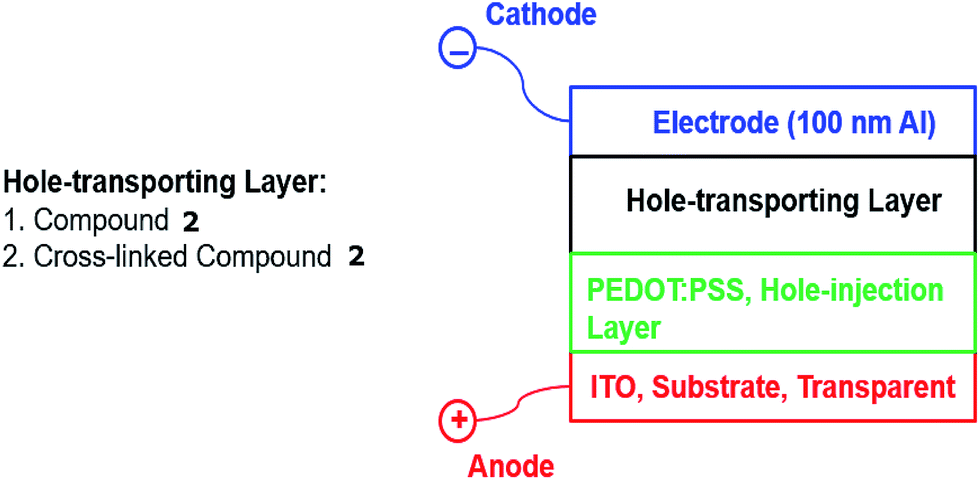 | ||
| Fig. 1 The schematic representation of hole-only test devices. | ||
The glass substrates were purchased from Ossila, with a pre-patterned layer of indium tin oxide (ITO, 150 nm) as the anode. Poly(3,4-ethylenedioxythiophene)polystyrene sulfonate (PEDOT:PSS, 40 nm) purchased from Sigma-Aldrich Corp., was spun on top of the ITO substrate at 2000 rpm.33 The triazatruxene layers of 2 [R = –CH2CON(CH2CHCH2)2] were deposited by spin-coating from chlorobenzene solutions on top of the PEDOT:PSS hole-injection layer and dried to remove the solvent. Excess triazatruxene was swabbed from the surface to expose the ITO contacts. Device 2 was exposed to 800 J cm−2 of UV fluence (365 nm), using the same conditions used to measure the cross-linking density in order to photochemically polymerise and crosslink the conjugated diene groups in a terminal position of the side chain of adjacent monomers. An aluminium layer (100 nm) was deposited by thermal evaporation at a vacuum of 8 × 10⁻⁶ mbar to form the device cathode. The cathode was covered with a thin layer of epoxy resin and a microscope cover slip was placed on top of the resin, which was then polymerised with a pulse of UV light to encapsulate the test device from atmospheric oxygen and moisture. These two hole-only diode test devices were operated using a voltage of 0–10 V, which is consistent with the operation of commercial OLEDs. A Keithley 2401 source meter controlled by Labview 2012 program was used to record the magnitude of the current density against applied voltage.
3 Results and discussion
3.1 Energy levels
Triazatruxene 1 [R = –(CH2)4CON(CH2CHCH2)2] and 2 [R = –CH2CON(CH2CHCH2)2] exhibit appropriate HOMO levels, see Table 1, in relation to PEDOT:PSS and common organic electroluminescent materials, for them to act as efficient hole-transport layers in plastic electronic devices, such as OLEDs, for example.33 They exhibit larger values of the band gap than many common hole-transport materials as shown by the UV-Vis onset values recorded in Fig. 2 and 3. The calculated LUMO levels are high-lying and should result in good electron-blocking properties. As expected, the energy levels are similar for both triazatruxene derivatives 1 and 2, due to the fact that the highly conjugated aromatic core of these triazatruxene derivatives, rather than the three flexible side chains, will determine their electronic properties due to overlap of the molecular orbitals of the aromatic cores and π–π stacking.
 | ||
| Fig. 2 (a) and (b) UV-Vis absorption spectra of monomer 1 [R = –(CH2)4CON(CH2CHCH2)2] (unexposed) and of the corresponding polymer network formed by its exposure to UV radiation (365 nm) at two different fluences (100 J cm−2 and 400 J cm−2, respectively) before and after washing with chlorobenzene. | ||
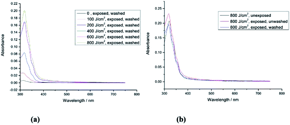 | ||
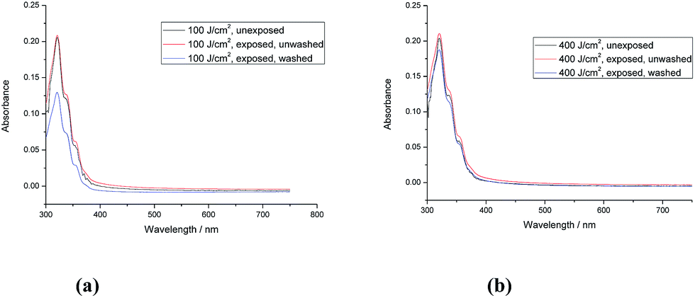
| Fig. 3 (a) UV-Vis absorption spectra of monomer 2 [R = –CH2CON(CH2CHCH2)2] (unexposed) and of the corresponding polymer network formed by its exposure to UV radiation (365 nm) at different fluences (100 J cm−2, 200 J cm−2, 400 J cm−2, 600 J cm−2 and 800 J cm−2) followed by washing with chlorobenzene and (b) UV-Vis absorption spectra of monomer 2 [R = –CH2CON(CH2CHCH2)2] (unexposed) and of the corresponding polymer network formed by its exposure to UV radiation at a fluence of 800 J cm−2 before and after washing with chlorobenzene. | ||
3.2 UV-Vis spectra before and after photochemical crosslinking
The polymer network formed by exposure of the triazatruxene monomer 1 [R = –(CH2)4CON(CH2CHCH2)2] to UV-radiation at a relatively low fluence (400 J cm−2) exhibits a relatively high crosslink yield (90.0%). The UV-Vis absorption spectra of the monomer 1 and the corresponding polymer networks formed by its photopolymerisation under UV light (365 nm), shown in Fig. 2a and b, reveal that the first major absorption peak for both the monomer and the polymer networks, as expected, appears at a similar wavelength, i.e., ca. 370 nm, as the aromatic chromophore responsible for the absorption peaks is the same one in each case. The similarity of the UV-vis absorption spectra of monomer 1 and the photochemically polymerized and crosslinked layers formed by its illumination with UV light (100 J cm−2 and 400 J cm−2), see Fig. 2a and b, respectively, suggests that no significant photodegradation of monomer 1 occurs during the UV exposure even at relatively high levels of fluence. However, the degree of polymerisation of polymer network formed at low fluence (100 J cm−2) is quite low (62.8%), whereas the degree of polymerisation of the corresponding polymer network formed at a higher fluence (400 J cm−2) is significantly higher and can, for practical purposes, be regarded as almost complete (90.0%). The photochemically crosslinked layers of 1 washed with chlorobenzene to remove any non-crosslinked material, i.e., monomer 1, reflect this difference in the crosslink density of the two layers. A relatively significant reduction in the intensity of the main UV-Vis absorbance peak is observed after washing of the polymer network formed from exposure of monomer 1 at low fluence (100 J cm−2), see Fig. 2a. However, the intensity of the main absorption peak of the polymer network formed by a similar exposure at a higher fluence (400 J cm−2) and then washed with chlorobenzene is only slightly lower, after washing, see Fig. 2b. This observation leads to the conclusion that a relatively high degree of polymerisation (90.0%) of monomer 1 [R = –(CH2)4CON(CH2CHCH2)2], with relatively long, flexible side chains, is sufficient to form an insoluble and intractable, thin, solid film on a device substrate.
The UV-Vis absorption spectra of monomer 2 (unexposed) and those of the polymer networks formed by exposure of monomer 2 to UV radiation at different fluences (100 J cm−2, 200 J cm−2, 400 J cm−2, 600 J cm−2 and 800 J cm−2) followed by washing with chlorobenzene are shown in Fig. 3a. Monomer 2 with a short side chain [R = –CH2CON(CH2CHCH2)2] requires double the fluence (800 J cm−2) of UV radiation (365 nm) to form an insoluble layer of highly crosslinked polymer network, see Fig. 3b, and to achieve a similar crosslink yield (87.4%) to that of the polymer network formed from monomer 1 (90%) with a longer side chain [R = –(CH2)4CON(CH2CHCH2)2]. The minimum fluence for sufficient photopolymerisation of non-conjugated dienes often depends on the freedom of movement of the flexible photopolymerisable side-groups.44 Therefore, the non-conjugated dienes at the end of a short side chain in monomer 2 [R = –CH2CON(CH2CHCH2)2] are more likely to be limited in their ability to react with adjacent photopolymerisable end-groups than those in 1 [R = –(CH2)4CON(CH2CHCH2)2] with a long side chain as illustrated in Fig. 2 and 3.
3.3 Hole-only diode test devices
The current density (I) plotted against the voltage (V) for hole-only test diodes incorporating either monomer 2 (black curve) or its corresponding polymer network (red curve) after exposure to UV radiation (365 nm) at a fluence of 800 J cm−2 is shown in Fig. 4. It can be seen from the I–V plots of the two hole-only diode test devices, shown in Fig. 4, that there is no reduction in the current density before (black curve) and after (red curve) monomer 2 has been photopolymerised to form a highly crosslinked polymer network. This is a very positive result as it is often observed that polymerisation of monomers with more than one polymerisable group, forming a highly crosslinked polymer network, results in a reduction in the charge-carrier mobility due to the disruption of the molecular order within the thin layer as the polymerisable end-groups form a covalently bonded polymer backbone and/or to the formation of both shallow and deep traps for charge carriers.41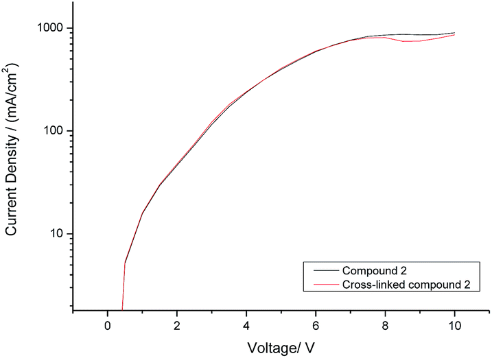 | ||
| Fig. 4 Current density vs. voltage (I–V) curve for hole-only test diodes incorporating either monomer 2 (black curve) or its corresponding polymer network (red curve) after exposure to UV radiation at a fluence of 800 J cm−2. | ||
Monomer 2 [R = –CH2CON(CH2CHCH2)2] was used in the hole-only diode test devices rather than monomer 1 [R = –(CH2)4CON(CH2CHCH2)2] due to the former's superior film forming properties, which is probably attributable to its much higher melting point compared to that of the latter with much longer flexible side chains, see ESI.† The relatively long side chains of monomer 1 [R = –(CH2)4CON(CH2CHCH2)2] reduce the degree of intermolecular packing and interaction between the large aromatic cores of the triazatruxene moiety and thereby give rise to a viscous oil at room temperature. Monomer 1 when spin-coated from chlorobenzene solution would aggregate on the PEDOT:PSS substrate surface and form regions of uncovered PEDOT:PSS, presumably due to the hydrophobic nature of the monomer, hydrophilic nature of PEDOT:PSS and the presence of a room temperature liquid that could move across the substrate surface.
A wide range of triarylamines has been extensively studied as hole-transport materials in commercial OLEDs due to the ready oxidation of the nitrogen centre to form stable radical cation species for the efficient transport of holes.45–49 Therefore, the star-shaped triarylamine monomer 3 with three non-conjugated diene end-groups, Fig. 5, was chosen to compare the hole-transport performance of its photochemically crosslinked polymer networks and that of the corresponding polymer networks formed by the photochemical polymerization and crosslinking under identical conditions, i.e., 800 J cm−2, of the triazatruxene monomer 2 with similar non-conjugated diene end-groups attached via flexible side groups to the aromatic molecular core.
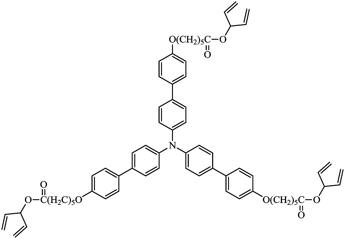 | ||
| Fig. 5 Chemical structure of triarylamine monomer 3. | ||
A comparison of the current density vs. voltage (I–V) plots of the hole-only diode test devices incorporating the triazatruxene 2 and triarylamine 3, as well as those for the corresponding highly crosslinked polymer networks, is shown in Fig. 6. It can be seen clearly that both of the hole-only diode test devices incorporating the triarylamine monomer 3 and its highly crosslinked polymer network (green and blue curve, respectively) exhibit a lower current density – and hence lower hole-carrier mobility – than those test devices incorporating the corresponding non-crosslinked triazatruxene monomer 2 and its highly crosslinked polymer network (black and red curve, respectively). However, the current density at the same voltage of the hole-only diode test devices incorporating a layer of polymer network formed by the photochemical polymerization and crosslinking of the triarylamine monomer 3 (blue curve) is much lower than that of the corresponding test device incorporating the monomer 3 (green curve) as the hole-transport layer. This fact may be due to the disruption of the molecular order within the layer as the non-conjugated diene end-groups react with each other to form a non-linear polymer backbone, thereby disrupting the planar packing of the aromatic cores due to inter-annular twisting of the triarylamine core.
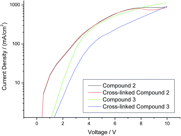 | ||
| Fig. 6 Current density vs. voltage (I–V) for hole-only diode test devices incorporating unexposed layers of monomers 2 and 3 and that of the corresponding test devices incorporating the corresponding polymer networks photochemically crosslinked at the same fluence (800 J cm−2) of UV irradiation to form hole transport layers as intractable and insoluble thin solid layers. | ||
We believe this is the first time that hole-only devices have retained similar current density profiles after the photochemical cross-linking process using non-conjugated dienes. Previous work using cross-linkable oxetane groups have successfully demonstrated this effect, but this has been dependent on the presence of a cationic photo-initiator, usually OPPI.50–53
4 Conclusions
Novel photopolymerisable triazatruxenes incorporating non-conjugated dienes at the end of flexible side chains were synthesised using simple N-substitution reactions. A minimal length of the aliphatic spacer is required to produce highly crosslinked layers at relatively low UV fluence. Photochemical initiator-free cross-linking of a triazatruxene monomer does not lead to any reduction of current density, i.e., charge carrier mobility, in hole-only diode test devices, before and after the UV exposure required to form a highly crosslinked, insoluble and stable polymer network. Similar test devices incorporating a standard photochemically crosslinked triaryl-amine hole-transport layer reveal a reduced current density under the same photochemical crosslinking conditions. These triazatruxenes monomers exhibit the desired energy levels for efficient charge-carrier mobility. A combination of these properties renders these triazatruxene derivatives as promising candidates for optimization as highly efficient hole-transport materials in multilayer plastic electronic applications.Conflicts of interest
There are no conflicts of interest to declare.Acknowledgements
The China Scholarship Council and the University of Hull are thanked for their support of a PhD studentship for Dr G. Hu.Notes and references
- B. G. Kim, E. J. Jeong, J. W. Chung, S. Seo, B. Koo and J. Kim, Nat. Mater., 2013, 12, 659 CrossRef CAS PubMed.
- M. Drack, I. Graz, T. Sekitani, T. Someya, M. Kaltenbrunner and S. Bauer, Adv. Mater., 2015, 27, 34 CrossRef CAS PubMed.
- S. Savagatrup, A. D. Printz, T. F. O'Connor, A. V. Zaretski and D. J. Lipomi, Chem. Mater., 2014, 26, 3028 CrossRef CAS.
- H. C. Moon, T. P. Lodge and C. D. Frisbie, J. Am. Chem. Soc., 2014, 136, 3705 CrossRef CAS PubMed.
- S. R. Park, D. H. Shin, S. M. Park and M. C. Suh, RSC Adv., 2017, 7, 28520 RSC.
- H. Wang, L. Xie, Q. Peng, L. Meng, Y. Wang, Y. Yi and P. Wang, Adv. Mater., 2014, 26, 5198 CrossRef CAS PubMed.
- H. Liu, Q. Bai, W. Li, Y. Guo, L. Yao, Y. Gao, J. Li, P. Lu, B. Yang and Y. Ma, RSC Adv., 2016, 6, 70085 RSC.
- D. Sun, Z. Ren, M. R. Bryce and S. Yan, J. Mater. Chem. C, 2015, 3, 9496 RSC.
- F. C. Krebs, N. Espinosa, M. Hosel, R. R. Sondergaard and M. Jorgensen, Adv. Mater., 2014, 26, 29 CrossRef CAS PubMed.
- S. Gelinas, A. Rao, A. Kumar, S. L. Smith, A. W. Chin, J. Clark, T. S. van der Poll, G. C. Bazan and R. H. Friend, Science, 2014, 343, 512 CrossRef CAS PubMed.
- Y. J. Chen, S. H. Yang and C. S. Hsu, Chem. Rev., 2009, 109, 5868 CrossRef PubMed.
- H. P. Kim, S. J. Lee, A. R. B. M. Yusoff and J. Jang, RSC Adv., 2016, 6, 28599 RSC.
- D. Zhou, J. Liu, L. Chen, H. Xu, X. Cheng, F. Wu and Y. Chen, RSC Adv., 2017, 7, 24345 RSC.
- A. Benito-Hernandez, U. K. Pandey, E. Cavero, R. Termine, E. M. Garcia-Frutos, J. L. Serrano, A. Golemme and B. Gomez-Lor, Chem. Mater., 2013, 25, 117 CrossRef CAS.
- Z. Lu, C. Li, T. Fang, G. Li and Z. Bo, J. Chem. Mater. A, 2013, 1, 7657 RSC.
- J. Luo, B. Zhao, J. Shao, K. A. Lim, H. S. O. Chan and C. Chi, J. Mater. Chem., 2009, 19, 8327 RSC.
- M. Talarico, R. Termine, E. M. Garcia-Frutos, A. Omenat, J. L. Serrano, B. Gomez-Lor and A. Golemme, Chem. Mater., 2008, 20, 6589 CrossRef CAS.
- W. Y. Lai, Q. Q. Chen, Q. Y. He, Q. L. Fan and W. Huang, Chem. Commun., 2006, 1959 RSC.
- L. Wang, Q. Fang, Q. Lu, S. J. Zhang, Y. Y. Jin and Z. Q. Liu, Org. Lett., 2015, 17, 4164 CrossRef CAS PubMed.
- B. Gomez-Lor, B. Alonso, A. Omenat and J. L. Serrano, Chem. Commun., 2006, 5012 RSC.
- M. Reig, J. Puigdollers and D. Velasco, J. Mater. Chem. C, 2015, 3, 506 RSC.
- F. Gallego-Gomez, E. M. Garcia-Frutos, J. M. Villalvilla, J. A. Quintana, E. Gutierrez-Puebla, A. Monge, M. A. Diaz-Garcia and B. Gomez-Lor, Adv. Funct. Mater., 2011, 21, 738 CrossRef CAS.
- B. Zhao, B. Liu, R. Q. Png, K. Zhang, K. A. Lim, J. Luo, J. Shao, P. K. H. C. Chi and J. Wu, Chem. Mater., 2010, 22, 435 CrossRef CAS.
- E. M. Garcia-Frutos and B. Gomez-Lor, J. Am. Chem. Soc., 2008, 130, 9173 CrossRef CAS PubMed.
- E. M. Garcia-Frutos, A. Omenat, J. Barbera, J. L. Serrano and B. Gomez-Lor, J. Mater. Chem., 2011, 21, 6831 RSC.
- C. Ruiz, E. M. Garcia-Frutos, D. A. da S. Filho, J. T. L. Navarrete, M. C. R. Delgado and B. Gomez-Lor, J. Phys. Chem. C, 2014, 118, 5470 CAS.
- Q. Ye, J. Chang, J. Shao and C. Chi, J. Mater. Chem., 2012, 22, 13180 RSC.
- F. Wang, X. C. Li, W. Y. Lai, Y. Chen, W. Huang and F. Wudl, Org. Lett., 2014, 16, 2942 CrossRef CAS PubMed.
- Y. F. Xie, S. Y. Ding, J. M. Liu, W. Wang and Q. Y. Zheng, J. Mater. Chem. C, 2015, 3, 10066 RSC.
- Y. Zou, J. Zou, T. Ye, H. Li, C. Yang, H. Wu, D. Ma, J. Qin and Y. Cao, Adv. Funct. Mater., 2013, 23, 1781 CrossRef CAS.
- W. Wu, R. Tang, Q. Li and Z. Li, Chem. Soc. Rev., 2015, 44, 3997 RSC.
- X. Y. Liu, T. Usui and J. Hanna, Chem. Mater., 2014, 26, 5437 CrossRef CAS.
- H. Tang, C. M. Hessel, J. Wang, N. Yang, R. Yu, H. Zhao and D. Wang, Chem. Soc. Rev., 2014, 43, 4281 RSC.
- A. W. Hall, M. Godber, J. K. M. Blackwood, P. E. Y. Milne and J. W. Goodby, J. Mater. Chem., 2004, 14, 2593 RSC.
- W. C. Tsoi, M. O'Neill, M. P. Aldred, S. P. Kitney, P. Vlachos and S. M. Kelly, Chem. Mater., 2007, 19, 5475 CrossRef CAS.
- N. Aizawa, Y. J. Pu, T. Chiba, S. Kawata, H. Sasabe and J. Kido, Adv. Mater., 2014, 26, 7543 CrossRef CAS PubMed.
- I. Osken, A. S. Gundogan, E. Tekin, M. S. Eroglu and T. Ozturk, Macromolecules, 2013, 46, 9202 CrossRef CAS.
- S. Hofle, A. Schienle, M. Bruns, U. Lemmer and A. Colsmann, Adv. Mater., 2014, 26, 2750 CrossRef PubMed.
- G. Li, Z. K. Tan, D. Di, M. L. Lai, L. Jiang, J. H. W. Lim, R. H. Friend and N. C. Greenham, Nano Lett., 2015, 15, 2640 CrossRef CAS PubMed.
- A. Liedtke, M. O'Neill, A. Wertmöller, S. P. Kitney and S. M. Kelly, Chem. Mater., 2008, 20, 3579 CrossRef CAS.
- M. O'Neill and S. M. Kelly, Adv. Mater., 2011, 23, 566 CrossRef PubMed.
- A. Cipiciani, S. Clementi, P. Linda, G. Marino and G. Savelli, J. Chem. Soc., Perkin Trans. 2, 1977, 1284 RSC.
- S. Kato, S. Shimizu, A. Kobayashi, T. Yoshihara, S. Tobita and Y. Nakamura, J. Org. Chem., 2014, 79, 618 CrossRef CAS PubMed.
- P. Strohriegl, D. Hanft, M. Jandke and T. Pfeuffer, Mater. Res. Soc. Symp. Proc., 2002, 709, 31 CAS.
- C. Lambert, G. Noll and J. Schelter, Nat. Mater., 2002, 1, 69 CrossRef CAS PubMed.
- N. Satoh, J. S. Cho, M. Higuchi and K. Yamamoto, J. Am. Chem. Soc., 2003, 1225, 8104 CrossRef PubMed.
- H. J. Yen, H. Y. Lin and G. S. Liou, Chem. Mater., 2011, 23, 1874 CrossRef CAS.
- Y. Su, X. Wang, X. Zheng, Z. Zhang, Y. Song, Y. Sui, Y. Li and X. Wang, Angew. Chem., 2014, 126, 2901 CrossRef.
- E. Busseron, J. J. Cid, A. Wolf, G. Du, E. Moulin, G. Fuks, M. Maaloum, P. Polavarapu, A. Ruff, A. K. Saur, S. Ludwigs and N. Giusepone, ACS Nano, 2015, 9, 2760 CrossRef CAS PubMed.
- K. Meerholz, 246th National Meeting of the American-Chemical-Society, 2013, vol. 246, p. 173 Search PubMed.
- G. Liaptsis, D. Hertel and K. Meerholz, Angew. Chem., Int. Ed., 2013, 52, 9563 CrossRef CAS PubMed.
- G. Liaptsis and K. Meerholz, Adv. Funct. Mater., 2013, 23, 359 CrossRef CAS.
- S. Feser and K. Meerholz, Chem. Mater., 2011, 23, 5001 CrossRef CAS.
Footnote |
| † Electronic supplementary information (ESI) available. See DOI: 10.1039/c8ra00830b |
| This journal is © The Royal Society of Chemistry 2018 |