
 Open Access Article
 This Open Access Article is licensed under a
 Creative Commons Attribution 3.0 Unported Licence
Structures and properties of Mg0.95Mn0.01TM0.04O (TM = Co, Ni, and Cu) nanoparticles synthesized by sol–gel auto combustion technique
M. A. Dar and
Dinesh Varshney *
*
Materials Science Laboratory, School of Physics, Vigyan Bhavan, Devi Ahilya University, Khandwa Road Campus, Indore 452001, India. E-mail: vdinesh33@rediffmail.com; Fax: +91-731-2467028; Tel: +91-731-2467028
First published on 17th April 2018
Abstract
The room temperature structural, optical and dielectric properties of Mg0.95Mn0.05O and Mg0.95Mn0.01TM0.04O (TM = Co, Ni, and Cu) nanoparticles are reported. All transition metal nanocrystalline samples were successfully prepared by sol–gel auto combustion method. X-ray powder diffraction patterns at room temperature confirmed the formation of single-phase cubic structure with an Fm![[3 with combining macron]](https://www.rsc.org/images/entities/char_0033_0304.gif) m space group for all prepared samples. Slight variation in the lattice parameter of TM doped Mg0.95Mn0.05O has been observed. Using Rietveld refinement of XRD data, the space group and lattice parameters are determined. Scanning electron microscopy (SEM) measurements were performed to understand the morphology and grain size of the Mg0.95Mn0.01TM0.04O (TM = Co, Ni, and Cu) nanocrystals. The estimated band gaps as calculated by using UV-Vis spectroscopy are found to be 3.59, 3.61, 5.63 and 3.55 eV for Mg0.95Mn0.05O and Mg0.95Mn0.01TM0.04O (TM = Co, Ni, and Cu) nanocrystals, respectively. Both dielectric constant and dielectric loss is found to decrease due to TM (transition metal) doping. The ac conductivity is found to increase with increase in frequency. Electric modulus spectra reflect the contributions from grain effects: the large resolved semicircle arc caused by the grain effect. The results obtained in this study were discussed comparatively with those cited in the literature.
m space group for all prepared samples. Slight variation in the lattice parameter of TM doped Mg0.95Mn0.05O has been observed. Using Rietveld refinement of XRD data, the space group and lattice parameters are determined. Scanning electron microscopy (SEM) measurements were performed to understand the morphology and grain size of the Mg0.95Mn0.01TM0.04O (TM = Co, Ni, and Cu) nanocrystals. The estimated band gaps as calculated by using UV-Vis spectroscopy are found to be 3.59, 3.61, 5.63 and 3.55 eV for Mg0.95Mn0.05O and Mg0.95Mn0.01TM0.04O (TM = Co, Ni, and Cu) nanocrystals, respectively. Both dielectric constant and dielectric loss is found to decrease due to TM (transition metal) doping. The ac conductivity is found to increase with increase in frequency. Electric modulus spectra reflect the contributions from grain effects: the large resolved semicircle arc caused by the grain effect. The results obtained in this study were discussed comparatively with those cited in the literature.
1. Introduction
Nanostructures have potential applications in modern science and technology due to their intriguing structural and optical properties.1,2 Recently, nanostructures based on oxides have received considerable attention from researchers of the fields of material science, physics and chemistry3,4 due to the presence of oxygen, a highly electronegative element, which exhibits the tendency of pulling the bonding electrons towards itself and away from the other elements thereby inducing substantial electric field at the interatomic scale.5Nanomaterials based on metal oxides with high surface to volume ratio have allured considerable interest from the research and scientific community due to their conceivable applications in the field of optoelectronics, nanoelectronics and sensing devices. In particular, magnesium oxide (MgO) is a fascinating basic oxide that has potential applications in catalysis, adsorption, synthesis of refractory ceramics,6,7 nano electronics, optoelectronics and sensing devices8 and superconductor products.9
Adsorption, catalyst supports, and optical sensors are the areas where metal oxides are especially used. Besides these, they are also used in biocompatibility, bioimaging10 and many other fields by virtue of their exceptional nanosized structures, superior chemical, morphological and optical band characteristics.11 The quantum size effect generated by an increase in the band gap due to a decrease in the quantum allowed state leads to the change in the electrical and optical characteristics of nanosized particles, which in other senses improves the surface and interface effects.12
MgO as ceramic has been focused due to its applicability in several areas. MgO is an accepted photocatalyst with exceptional chemical, mechanical, optical and electrical properties. Besides, the inexpensiveness and non-toxicity were regarded as the main reason for the acceptability of MgO materials in modern age of materials. Keeping in view its photocatalytic properties, excellent dielectric properties, the multidimensional applications of MgO such as refractory, paint, translucent ceramics, plasma display panel, absorbent for many pollutants and superconductor products were explored.13–15
Magnesium oxide (MgO) exhibits a large band gap of 7.7 eV, excitonic binding energy of ∼80 MeV and posses high transmission in the ultraviolet (Uv) region.16 Therefore, MgO can be used to enhance the band gap of ZnO by forming its solid solution with MgO. Since the phase purity, homogeneity, particle size, morphology, as well as crystallinity are the tools to determine the optical properties of materials, the care, control and selection of the method to synthesize the material is of the utmost importance.
A large number of techniques were commonly used for the preparation of MgO powders, such as sol–gel method,17 flame spray pyrolysis,18 chemical vapour deposition,19 co-precipitation method20 etc. Manganese (Mn) enters the MgO crystal preferentially in the divalent charge state occupying cubic Mg sites. Depending on the thermal history of the crystal, higher valence states are possible by virtue of which charge compensation can be achieved by Mg vacancies.21 Among the different methods, the sol–gel method is the most effective method to prepare the nanopowders of metal oxides as it is fast, economic and low temperature is required by this method to synthesize the nanosized samples.
The ability to obtain single-phase metal oxide magnetic nanoparticles with controllable particle size and size distribution improves its adequacy in a wide range of technological applications. The sol–gel auto combustion was utilized to synthesize the metal oxide nanoparticles by various researchers in this field. NiFe2O4 nanoparticles were prepared by a simple and cost-effective polyvinylpyrrolidone (PVP) assisted sol–gel auto-combustion method.22 Recently this method also shows option to synthesize advanced spinel ferrite one-dimensional (1D) and two-dimensional (2D) nano-structures.23,24 La0.67Sr0.33MnO3 nanoparticles were also successfully synthesized via the sol–gel auto-combustion technique.25
Herein, the Mg0.95Mn0.05O and transition metal doped Mg0.95Mn0.01TM0.04O (TM = Co, Ni, and Cu) nanoparticles were prepared by a sol–gel auto combustion method. The structural, optical and electric properties of as prepared powders have been studied by X-ray diffraction (XRD), scanning electron microscopy (SEM), ultra-violet visible spectrum (UV-Vis), Fourier transformation infra red (FT-IR) spectroscopy and dielectric measurements. The main goal of this study is to investigate the effect of TM doping on the structural, vibrational, optical and dielectric properties of Mg0.96Mn0.04O nanoparticles. For optoelectronic device applications, the controlled band gap is of the utmost importance. In this regard, we made an effort to tune the band gap with different TM doping using UV-Vis spectroscopy.
2. Experimental details
2.1 Synthesis
The pristine Mg0.95Mn0.05O and transition metal doped samples of Mg0.95Mn0.01TM0.04O (TM = Co, Ni and Cu) nanoparticles were prepared by sol–gel auto combustion method. All the chemicals were obtained from Merck, India (Analytical grade) and used as such without further purification. The typical synthesis procedure for pure and Co-doped Mg0.95Mn0.05O is as follows: The aqueous solution of Co doped Mg0.95Mn0.05O salt were freshly prepared by taking metal nitrates such as magnesium nitrate [Mg (NO3)2·6H2O], manganese nitrate [Mn (NO3)2·6H2O] and cobalt nitrate [Co (NO3)2·6H2O] in appropriate molar ratio. Mg (NO3)2·6H2O were dissolved in 100 ml distilled water and calculated amount of Mn (NO3)2·6H2O and Co (NO3)2·6H2O were added to it. The nitrate salts are favoured as precursors, because they serve as water-soluble low temperature NO3− oxidant source for synthesis.When all the reactants are completely dissolved, citric acid was added to make a metal complex maintaining pH value at 11. The best about the present study is the preparation with the maintenance of pH and citric acid assistance to control reaction and particle size. Citric acid acted as a chelating agent and helps the reaction to proceed. The addition of citric acid dissolved the insoluble residue leading to the formation of a cation–citric acid complex. Further the nitrate salts are favored as precursors, because they serve as water-soluble low temperature NO3− oxidant source for synthesis. Many other fuels including DL-alanine, hydrazine, acrylic acid, carbo-hydrazide, ethylene glycol and polyacrylic acid have also shown great promises. The whole solution was stirred through magnetic beet using a magnetic stirrer for 5 hours at 80 °C temperature until the gel was obtained. The gel obtained was dried at 400 °C for 4 hours to remove water and solvent content. The synthesized MgO powder was white in colour. The powder was calcined in air at 600 °C for 10 h and then pressed into pellets of 10 mm diameter with 2 mm thickness. Finally, the pellets were sintered at 600 °C for 6 h. Similar procedure was adopted for the synthesis of all other transition metal doped samples.
The formation of Mg0.95Mn0.05O takes place according to procedure as follows:

2.2 Characterization
The crystal structure, type of phases and particle size of Mg0.95Mn0.05O and transition metal doped samples of Mg0.95Mn0.01TM0.04O (TM = Co, Ni, and Cu) nanoparticles were investigated by means of room temperature X-ray powder diffraction technique using Bruker D8-Advance X-ray diffractometer with CuKα1 (1.5406 Å) radiation. The XRD data were collected in the 2θ range from 10° ≤ 2θ ≤ 80° with a step size of 0.02° and a scanning rate of 2°/min. The X-ray generator was set at 40 kV and 40 mA power setting. Scanning electron microscope images were recorded with a Philips XL30 ESEM (environmental scanning electron microscope).Diffuse reflectance spectra were recorded in the wavelength range 200–850 nm using UV-Vis spectrometer (Perkin Elmer, Lambda 950 – USA to estimate energy band gap). Dielectric measurements were carried out as a function of frequency in the range of 1–10 MHz on Novocontrol alpha-A high performance frequency analyzer at room temperature. High purity silver conducting paste was used to coat on the pellets for better electrical contact for the dielectric measurements.
3. Results and discussion
3.1 Structural analysis
XRD analysis provides information about the structural characteristics of the material as the width and the intensity of the diffraction peaks depend on lattice strain, crystallite size and other imperfections such as stacking faults etc. The as prepared Mg0.95Mn0.05O based transition metal doped powders at the temperature of 600 °C have been structurally characterized by room temperature X-ray powder diffraction (XRD). The XRD patterns of Mg0.95Mn0.01TM0.04O (TM = Co, Ni, and Cu) = (Co, Ni and Cu) samples are shown in Fig. 1 in which all the samples present similar peak positions. The diffraction peaks of samples are indexed as (111), (200), (220), (311) and (222). All the samples exhibit the reflections corresponding to cubic MgO phase having space group Fmm.
 | ||
| Fig. 1 Powder X-ray diffraction pattern of Mg0.94Mn0.06O and Mg0.95Mn0.01TM0.04O (TM = Co, Ni, and Cu) metal oxide nano particles. | ||
The powders obtained showed a crystallized structures, which is matched with JCPDS PDF (no. 45-946) and consistent with earlier reports.26,27 All the samples are in single phase and no diffraction peaks from other species could be detected within measurement range. It means that the TM ion successfully occupies the lattice site rather than interstitial ones. One can observe a slight shift of the position in the diffraction peaks indicating a light variation in lattice parameters. The lattice parameters are calculated using the formula for cubic structure.
| 1/d2 = a/(h2 + k2 + l2) | (1) |
Here, d is the interplanar distance, h, k, l are the miller indices and ‘a’ is the lattice parameter. One can see the decrease of the lattice parameter from 0.4215 nm in the pristine Mg0.96Mn0.04O to about 0.42104 nm for Mg0.95Mn0.01TM0.04O. The decrease in the lattice parameters of Mg0.95Mn0.01Co0.04O and Mg0.95Mn0.01Ni0.04O as compared to pristine Mg0.95Mn0.05O is attributed to the lower ionic size of Co2+ (0.72 Å), Ni2+ (0.69 Å) and Cu2+ (0.72 Å), respectively than ionic radii of Mn2+ (80 Å) ion. This is in good agreement with previous reports.28
The width of the peak is inversely related to the crystallite size, which has been computed from the full width half maximum (FWHM) of the intense peak using the Debye–Scherer's formula:
d = 0.9λ/β![[thin space (1/6-em)]](https://www.rsc.org/images/entities/char_2009.gif) cosθ cosθ
| (2) |
In eqn (2), symbols as ‘λ’ is the wavelength of CuKα1 radiation and ‘β’ is the full width half maximum (FWHM) of the highest intense peak of diffracting angle 2θ. Table 1 shows the values of particle size (d) and lattice variables obtained from the diffraction patterns of the powdered samples of Mg0.95Mn0.05O and Mg0.95Mn0.01TM0.04O (TM = Co, Ni, and Cu). It was found that the crystallite size of samples lies in the range of 32.3–47.6 nm.
| Compounds | Space group | Lattice parameters | Particle size (nm) | Optical band gap (eV) |
|---|---|---|---|---|
| a (Å) | ||||
| Mg0.95Mn0.05O | Fd3m | 4.2150 (4) | 32.34 | 3.59 |
| Mg0.95Mn0.01Co0.04O | Fd3m | 4.2092 (4) | 24.00 | 3.61 |
| Mg0.95Mn0.01Ni0.04O | Fd3m | 4.2106 (4) | 34.86 | 5.63 |
| Mg0.95Mn0.01Cu0.04O | Fd3m | 4.2104 (4) | 47.60 | 3.55 |
No doubt, particle size is variable with temperature. On annealing the lattice defects and strains generally decreases, however, it can also cause coalescence of crystallites that result in increasing the average size of the nanoparticles. The nano particles of metal oxides in the range of 40–50 nm at around 600 °C are also earlier reported.29–31 In this work particle size is calculated using Debye–Scherer's formula: the width of the peak is inversely related to the crystallite size, which has been computed from the full width half maximum (FWHM) of the intense peak. Instrumental broadening is not considered in entire XRD measurement.
Rietveld analyses of the diffraction data collected at the room temperature were carried out using Full Prof refinement program for Mg0.95Mn0.05O and Mg0.95Mn0.01TM0.04O (TM = Co, Ni, and Cu) nanoparticles. The Pseudo Voigt function is selected to refine the shape of the peak. Background, peak width, peak shape, lattice parameters and atomic positions were refined in the analysis. The Rietveld refined X-ray diffraction (XRD) plots of all the samples under investigation are shown in Fig. 2. Rietveld refined plots further confirms that the pristine Mg0.95Mn0.05O is in single phase possessing cubic phase structure with Fmm space group. It is observed that there is no change in the crystal structure due to transition element doping in Mg0.95Mn0.05O. It indicates that the cubic phase is retained up to 5% doping of Co, Ni and Cu in Mg0.95Mn0.05O nanoparticles.
 | ||
| Fig. 2 Rietveld refined XRD patterns of Mg0.94Mn0.06O and Mg0.95Mn0.01TM0.04O (TM = Co, Ni, and Cu) metal oxide nano particles. | ||
The typical values of structural parameters in cubic co-ordinates for all samples refined by a standard Rietveld technique using FullProf refinement program are listed in Table 2 along with the values of the profile factor Rp, weighted profile factor Rwp, expected weighted profile factor Rexp, Bragg factor RB, structure factor RF, goodness of fit χ2 and goodness of fit (GOF) index. Here, red symbols are the observed profile; the black solid line is the calculated profile, tick marks below indicate the position of the allowed Bragg reflections, the blue line curve at the bottom gives the difference between the observed and calculated data. All these parameters were used as numerical criteria of the quality of the fit of calculated to experimental diffraction data.
| Sample Name | Mg0.95Mn0.05O | Mg0.95Mn0.01Ni0.04O | Mg0.95Mn0.01Co0.04O | Mg0.95Mn0.01Cu0.04O |
|---|---|---|---|---|
| Space group | Fmm |
Fmm |
Fmm |
Fmm |
| a (Å) | 4.2097 (4) | 4.2084 (4) | 4.2089 (4) | 4.2058 (4) |
| V (Å3) | 74.6039 | 74.5359 | 74.5618 | 74.6070 |
| ρ (g cm−3) | 4.2097 | 4.2084 | 4.2088 | 4.1254 |
| Rp | 25.8 | 25.8 | 38.5 | 37.6 |
| Rwp | 24.1 | 20.2 | 23.7 | 30.2 |
| Rexp | 13.8 | 11.00 | 18.00 | 13.00 |
| RBragg | 6.67 | 3.95 | 4.31 | 8.34 |
| Rf | 6.85 | 3.33 | 2.82 | 4.54 |
| GoF | 2 | 1.8 | 1.3 | 2.2 |
| χ2 | 3.036 | 3.30 | 1.73 | 3.7 |
3.2 Microstructural analysis
Fig. 3a–d shows the SEM images of the synthesized Mg0.95Mn0.05O and Mg0.95Mn0.01TM0.04O (TM = Co, Ni, and Cu) nanocrystals. All the three images illustrate that the synthesized materials are un-agglomerated with spherical morphology. In general, the growing nanocrystals are highly attractive due to large surface energy by virtue of their large surface to volume ratio resulting in the agglomeration of nanocrystals by Ostwald ripening process.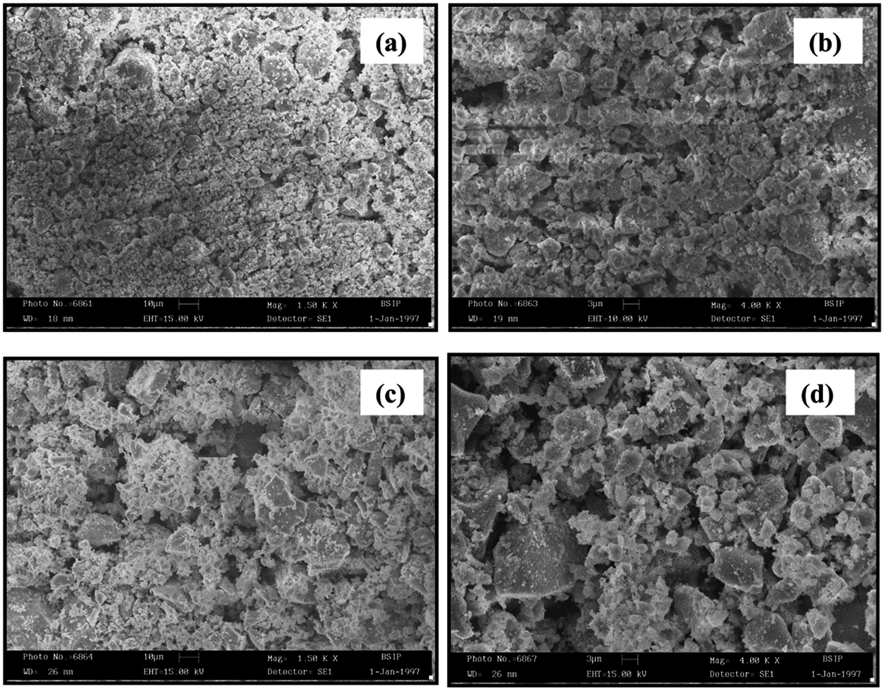 | ||
| Fig. 3 SEM images of Mg0.94Mn0.06O and Mg0.95Mn0.01TM0.04O (TM = Co, Ni, and Cu). | ||
Agglomeration process can be suppressed to control the size of nano crystallites by the introduction of organic molecules during the synthesis process as a capping agent. From SEM images, the average grain size for all four samples under investigation is in the range of 31–48 nm. The crystallite size determined from the SEM measurement is in good agreement with the size as obtained from the XRD.
In order to confirm the exact composition of the prepared nanocrystals, the EDAX analysis were carried out for Mg0.95Mn0.05O and Mg0.95Mn0.01TM0.04O (TM = Co, Ni, and Cu) nanocrystals (please see Fig. 4a–d). The EDAX analysis of Mg0.95Mn0.05O and Mg0.95Mn0.01TM0.04O confirms the presence of Co, Ni and Cu in the Mg0.95Mn0.05O system and its weight percentage is nearly equal to their nominal stoichiometry within the experimental error.
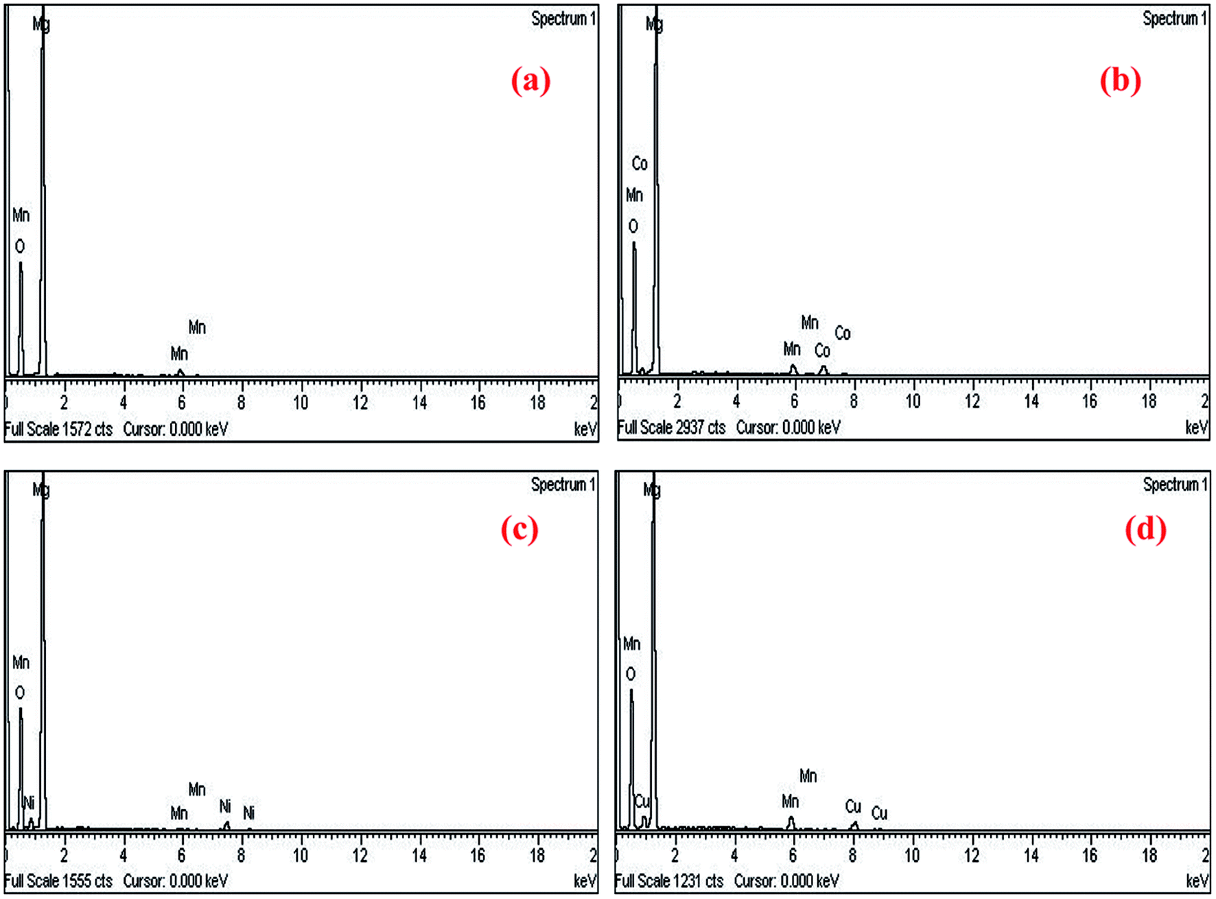 | ||
| Fig. 4 EDAX spectra showing elemental composition of Mg0.94Mn0.06O and Mg0.95Mn0.01TM0.04O (TM = Co, Ni, and Cu). | ||
Thus EDAX spectra show consistency with the experimental concentration used for all the samples. Fig. 4 revealed the presence of Mg, Mn, Co and O as the only elementary components with the absence of any extra element. This indicates that the CoO substitution in the Mg0.96Mn0.04O do not alter the structure of the host compound which may be attributed to the effective replacement of Mn site by the Co ion.
3.3 UV-Vis analysis
UV-visible absorption study is a powerful probe for investigating the effects of impurity doping on optical properties of semiconductor nano structures. The doped nanostructures are expected to have different optical characteristics as compare to pristine nanostructures. The optical diffuse reflectance spectra were recorded using diffuse reflectance spectroscopy to determine the optical band gaps of the as synthesized samples. All spectra were recorded in the range of 200–800 nm.In order to calculate the direct band gap, Tauc relation is used:
| (αhυ) = A(hυ − Eg)n | (3) |
In eqn (3), the notations α is the absorption coefficient, A is a constant, n = 1/2 for direct band gap semiconductor. The Eg values are determined by extrapolating the linear region of the (hυF(R))2 as functions of hυ. In other words, the hυ value of x-axis at (hυF(R))2 = 0 gives the band gap (Eg). Fig. 5 shows the plot for the percentage of reflection (hυF(R))2 as a function of band gap energy hυ (eV) for all the studied samples. An extrapolation of the linear region of a plot of (αhν)2 vs. hν gives the value of the optical band gap Eg (Fig. 5).
 | ||
| Fig. 5 UV-Visible spectra of Mg0.94Mn0.06O and Mg0.95Mn0.01TM0.04O (TM = Co, Ni, and Cu) nanopowders obtained at room temperature. | ||
The estimated band gaps were 3.59, 3.61, 5.63 and 3.55 eV for Mg0.95Mn0.05O and Mg0.95Mn0.01TM0.04O (TM = Co, Ni, and Cu) nanocrystals, respectively. The calculated value of optical band gap is found to vary from 3.59 eV for Mg0.95Mn0.05O to 3.55 eV for Mg0.95Mn0.01Cu0.04O. The band gaps of Co and Ni doped samples are greater than pristine Mg0.95Mn0.05O material. However, Cu doped sample has lower band gap than Mg0.95Mn0.05O. This suggests that decrease in the band gap of Cu-doped Mg0.95Mn0.05O nanoparticles is due to the incorporation of Cu into Mg0.95Mn0.05O matrix which alters the electronic structure leading to the appearance of intermediate energy level.32
Eg values of MgMnO nanoparticles increased with Ni content. The incorporation of Ni is accompanied by a systematic high-energy shift of the band gap extending down to the blue spectral range. The increase in the band gap or blue shift can be explained on the basis of the Burstein–Moss effect about filling the bottom of the conduction band depending on the increase in the carrier concentration. Therefore, the interstitial of Ni2+ in MgO lattice may cause an increase in the carrier concentration and the Fermi level moves closer to the conduction band with an increase in the carrier concentration. Consequently, the filling of the conduction band by electrons generally causes an increase in the optical band gap or blue shift. The same increase in Eg was also earlier reported.33 They reported a blue shift of the absorption edges from 3.22 eV (undoped ZnO) to 3.30 eV (5% Co-doped ZnO). Such an increase in the optical band gap is consistent with previous observations.34–36
3.4 Dielectric measurement
The dielectric constant and dielectric loss of a material are two basic criteria that a material must match for the better applicability and efficiency as they affect many optoelectronic and transport properties. Dielectric studies have been done on Mg0.95Mn0.05O and Mg0.95Mn0.01TM0.04O (TM = Co, Ni, and Cu) nanocrystals to investigate any variation of dielectric constant and dielectric loss with frequency and different transition metal ion doping.The dielectric properties of materials are characterized by the complex dielectric constant (ε) which is represented by ε = ε′ − jε′′. The real part (ε′) of dielectric constant is the measure of the amount of energy stored in a dielectric due to the applied field and the imaginary part (ε′′) of dielectric constant describes the dissipated energy in dielectric. The value of real part of dielectric constant (ε′) is calculated by using ε = Ct/(Aε0) where ε0 is the permittivity of free space, t is the thickness of pellet, A is the cross sectional area and C is the capacitance of pellet.
Fig. 6 shows the variation of dielectric constant (ε′) with frequency for Mg0.95Mn0.05O and Mg0.95Mn0.01TM0.04O (TM = Co, Ni, and Cu) at room temperature. At lower frequency the dispersion of dielectric constant was observed. The large value of dielectric constant at lower frequency observed is attributed to the grain boundary defects or the presence of oxygen vacancies.37 In addition to that, the large value of the dielectric constant is also due to the fact that the nanoparticles of Mg0.95Mn0.05O under the application of electric field act as nano dipoles. With the decrease in the size of nano particle, the particles per unit volume increases and thereby increases dipole moment per unit volume and hence the high dielectric constant.38 It is noticed that the dielectric constant is decreased in TM doped Mg0.95Mn0.05O as compared with pure Mg0.95Mn0.05O. The dielectric constant decreased in the whole applied frequency region with TM dopant up to 4%. Because, the polarization is decreased due to the formation of grains surrounded by insulating grain boundaries. The doping may create many defects into MgO, thus reduces the dielectric constant.
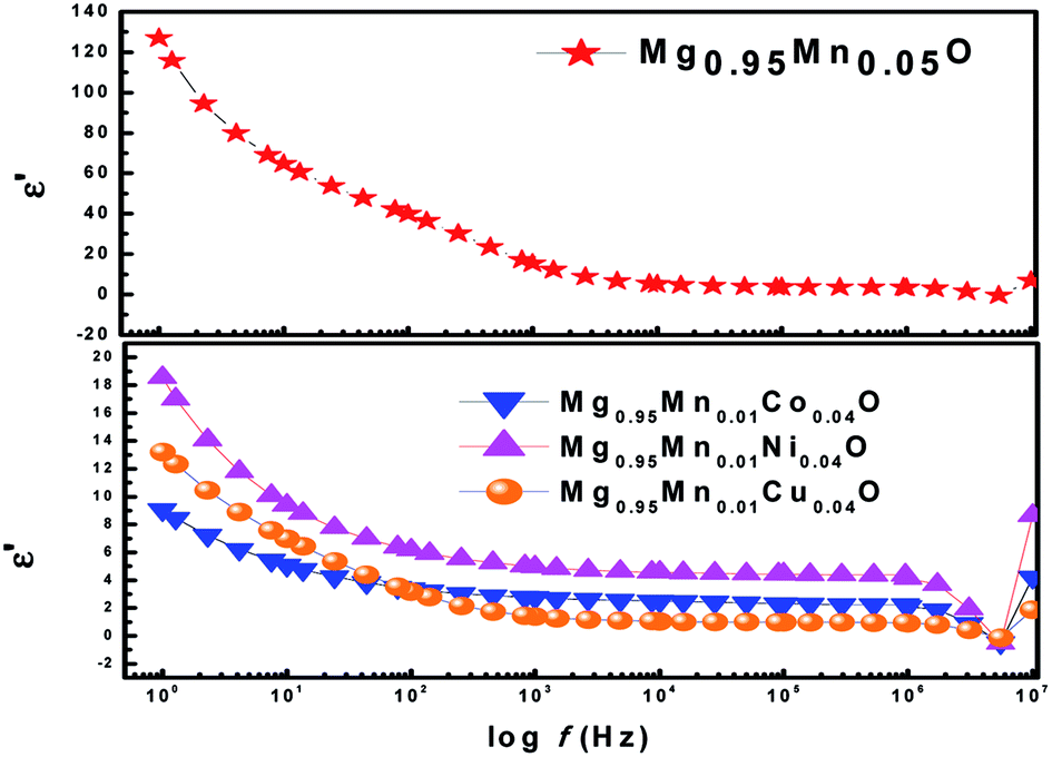 | ||
| Fig. 6 Variation of real part of dielectric constant with frequency of Mg0.94Mn0.06O and Mg0.95Mn0.01TM0.04O (TM = Co, Ni, and Cu) at room temperature. | ||
However, in the higher frequency regime i.e. frequency above 0.5 MHz, ε′ is independent of frequency. As beyond a certain frequency limit, the hopping between different metal ions cannot follow the changing field. Further, dielectric constant of Mg0.95Mn0.05O decreases due to Co, Ni and Cu doping at Mn-site. The lowest dielectric constant is observed for Mg0.95Mn0.01Co0.04O which is ∼9 at lower frequency and highest dielectric constant is obtained for pristine Mg0.95Mn0.05O of about 128.
The imaginary part (ε′′) of dielectric constant of Mg0.95Mn0.05O and Mg0.95Mn0.01TM0.04O (TM = Co, Ni, and Cu) nanocrystals shows a normal dielectric behaviour as observed earlier.39 We note that the imaginary part of dielectric constant (ε′′) shows a decreasing trend with increase in frequency (see Fig. 7), almost similar to real part of dielectric constant and loss tangent. This variation in imaginary part of dielectric constant (ε′′) with respect to frequency may be due to several factors; such as conduction mechanism (hopping of electron between Mn3+ and Mn2+), materials composition of sample, annealing temperature, grown technique and particle size.40
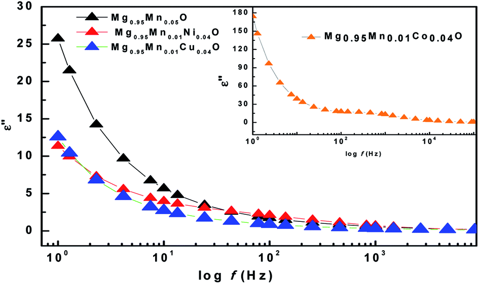 | ||
| Fig. 7 Variation of imaginary part of dielectric constant with frequency of Mg0.94Mn0.06O and Mg0.95Mn0.01TM0.04O (TM = Co, Ni, and Cu) at room temperature. | ||
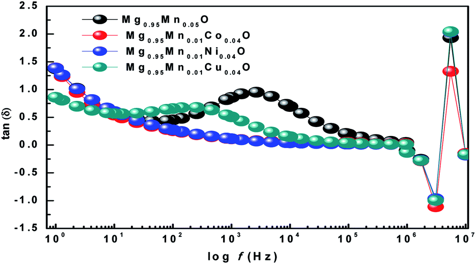
The ratio of energy dissipated and energy stored in the material determines the dielectric loss factor (tanδ) and variation of dielectric loss with frequency at room temperature is shown in Fig. 8. It shows that the dielectric loss (tanδ) decreases with the increase of frequency in all the samples. Wide peaks are observed in Mg0.95Mn0.05O and Mg0.95Mn0.01Cu0.04O samples which are believed to exist due to the resonance between the hopping frequency of charge carriers and applied frequency. No peak like behaviour is observed in Mg0.95Mn0.01Co0.04O and Mg0.95Mn0.01Ni0.04O samples as their resonance frequency lies beyond the measurement frequency range.41
 | ||
| Fig. 8 Variation of Dielectric Loss with frequency of Mg0.94Mn0.06O and Mg0.95Mn0.01TM0.04O (TM = Co, Ni, and Cu) at room temperature. | ||
In this work, we have observed that dielectric loss decreases at higher frequency which is due to suppression of domain wall motion. The dielectric loss is maximum at lower frequencies and is due to nearly equal hopping frequency between different ionic sites and the frequency of the applied field. Dielectric loss of the doped samples Mg0.95Mn0.01Co0.04O, Mg0.95Mn0.01Ni0.04O and Mg0.95Mn0.01Cu0.04O is slightly less than Mg0.95Mn0.05O, which is due to the decrease in dielectric constant as, described earlier.
The ac conductivity of pure Mg0.95Mn0.05O and Mg0.95Mn0.01TM0.04O (TM = Co, Ni, and Cu) nanoparticles is shown in Fig. 9. It is found that the ac conductivity progressively increases with the increase in the frequency of the applied ac field. This is because rising in frequency would improve the electron hopping frequency. The ac conductivity is initially high for pure Mg0.95Mn0.05O and found to be less in transition metal doped Mg0.95Mn0.01TM0.04O (TM = Co, Ni, and Cu) nanoparticles. The substitution of transition metal doping may initiate the defect ions, oxygen vacancies in the Mg0.95Mn0.05O nanoparticles and tends to segregate at the grain boundaries due to the diffusion at the time of sintering and cooling processes. These defects block the flow of charge carriers at the grain boundaries and cause decreases in the conductivity initially thereafter the conductivity of doped nanoparticles increases. Mg0.95Mn0.01Co0.04O has highest value of ac conductivity both at low and high frequencies as compared to other transition metal doped samples.
 | ||
| Fig. 9 Variation of ac conductivity as a function of frequency for Mg0.94Mn0.06O and Mg0.95Mn0.01TM0.04O (TM = Co, Ni, and Cu) at room temperature. | ||
The dielectric modulus plots of M′′ (= ε′′(ω)/[ε′(ω)2 + ε′′(ω)2]) as functions of M′ (=ε′(ω)/[ε′(ω)2 + ε′′(ω)2]) for various composition is shown in Fig. 10. Inset of Fig. 10 shows low frequency region modulus plot due to the grain boundary contribution. The large semicircle obtained in Mg0.95Mn0.01Co0.04O is believed to be induced by the grain effect, due to the smaller capacitance value dominated in the electric modulus spectra. On the other hand, the small semicircle obtained in Mg0.95Mn0.05O, Mg0.95Mn0.01Co0.04O and Mg0.95Mn0.01Cu0.04O might be attributed to the grain boundary effect. With the huge difference (orders of magnitude) between the resistive values of grains and grain boundaries, it is difficult to obtain two full semicircles for grains and grain boundary on the same scale in the impedance plot. Complex modulus analysis is suitable when materials have nearly similar resistance but different capacitance.42
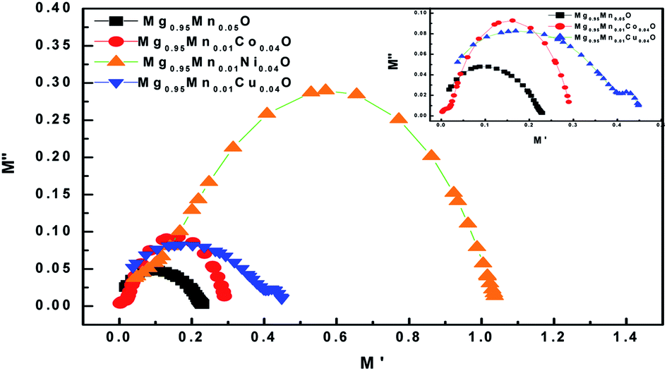 | ||
| Fig. 10 Cole–Cole plot for Mg0.94Mn0.06O and Mg0.95Mn0.01TM0.04O (TM = Co, Ni, and Cu) at room temperature. | ||
4. Conclusions
In summary, we have synthesized Mg0.95Mn0.05O and Mg0.95Mn0.01TM0.04O (TM = Co, Ni, and Cu) nanocrystalline samples using sol–gel auto combustion method. The structural, microstructural, optical, and dielectric properties were sensitively dependent on the incorporation of TM2+ ions into MgO matrix. X-ray diffraction (XRD) confirmed the single-phase cubic structure with Fmm space group for all prepared samples.
The calculated values of optical band gap vary from 3.59 eV for Mg0.95Mn0.05O to 3.55 eV for Mg0.95Mn0.01Cu0.04O. The lowest dielectric constant is observed for Mg0.95Mn0.01Co0.04O which is ∼9 at lower frequency and highest dielectric constant is obtained for pristine Mg0.95Mn0.05O of ∼128. Dielectric loss (tanδ) of Mg0.95Mn0.05O and Mg0.95Mn0.01Cu0.04O nanostructured materials decreases with increase in frequency having wide peaks in certain range of frequency, which is due to the resonance among the hopping frequency of charge carriers and applied frequency. Electric modulus spectra reflect the contributions from grain effects: the large resolved semicircle arc caused by the grain effect.
Conflicts of interest
There are no conflicts to declare.Acknowledgements
UGC-DAE-CSR, as an institute is acknowledged for extending its facilities. Authors acknowledge fruitful discussion with Dr V. Ganesan, Dr M. Gupta, Dr D. M. Phase, and Dr U. P. Deshpande of UGC-DAE CSR, Indore. Technical support from Mr Vinay K Ahire, UGC-DAE CSR, Indore is also gratefully acknowledged. Authors acknowledge MPCST, Bhopal (4836/CST/R&D/Phy&Engg Sc/2014) for financial assistance.References
- Y. Lin, A. Boker, J. He, K. Sill, H. Xiang, C. Abetz, X. Li, J. Wang, T. Emrick, S. Long, Q. Wang, A. Balazs and T. P. Russell, Nature, 2005, 34, 55 CrossRef PubMed.
- A. S. Arico, P. Bruce, B. Scrosati, J. M. Tarascon and W. V. Schalkwijk, Nat. Mater., 2005, 4, 366 CrossRef CAS PubMed.
- D. Varshney and S. Dwivedi, Mater. Res. Exp., 2015, 2, 106102 CrossRef.
- T. Prakash, R. Jayaprakash, C. Espro, G. Neri and E. Ranjith Kumar, J. Mater. Sci., 2014, 49, 1776 CrossRef CAS.
- D. Varshney and S. Dwivedi, Superlattices Microstruct., 2015, 86, 430 CrossRef CAS.
- S. Rajagopalan, S. Koper, S. Decker and J. Klabundek, J. Chem. Eur., 2002, 8, 2602 CrossRef CAS.
- S. Utampanya, K. J. Keabunde and J. R. Schlup, Chem. Mater., 1991, 3, 175 CrossRef.
- T. Jintakosol and P. Singjai, Curr. Appl. Phys., 2009, 9, 1288 CrossRef.
- G. Duan, X. Yang, J. Chen, G. Huang, L. Lu and X. Wang, Powder Technol., 2007, 172, 27 CrossRef CAS.
- M. Deepa, A. K. Srivastava and S. A. Agnihotry, Acta Mater., 2006, 54, 4583 CrossRef CAS.
- Y. G. Zhang, H. Y. He and B. C. Pan, J. Phys. Chem. C, 2012, 116, 23130 CAS.
- J. Wang, X. Yunhua, M. Hojamberdiev, J. Peng and G. Zhu, J. Noncryst. Solid, 2009, 355, 903 CrossRef CAS.
- C. Jin, H. Kim, S. Park and C. Lee, J. Alloys Compd., 2012, 541, 163 CrossRef CAS.
- P. B. Devaraja, D. N. Avadhani, S. C. Prashantha, H. Nagabhushana, S. C. Sharma, B. M. Nagabhushana, H. P. Nagaswarupa and H. B. Premkumar, Spectrochim. Acta, Part A, 2014, 121, 46 CrossRef CAS PubMed.
- J.-W. Ok, D.-K. Lee, D.-H. Kim, H. J. Lee, H.-J. Lee and C.-H. Park, Thin Solid Films, 2009, 517, 4152 CrossRef CAS.
- G. H. Ning, X. P. Zhao and J. Li, Opt. Mater., 2004, 27, 1 CrossRef CAS.
- T. Qiu, X. L. Wu, F. Y. Jin, A. P. Huang and P. K. Chu, Appl. Surf. Sci., 2007, 253, 3987–3990 CrossRef CAS.
- X. Yi, W. Wenzhong, Q. Yitai, Y. Li and C. Zhiwen, Surf. Coat. Technol., 1996, 82, 291 CrossRef CAS.
- Y. Li, Y. Bando and T. Sato, Chem. Phys. Lett., 2002, 359, 141 CrossRef CAS.
- P. Sivakumar, R. Ramesh, A. Ramanand, S. Ponnusamy and C. Muthamizhchelvan, Mater. Lett., 2011, 65, 1438 CrossRef CAS.
- B. Henderson and T. P. P. Hall, Proc. Phys. Soc., 1967, 90, 511 CrossRef CAS.
- P. Sivakumar, R. Ramesh, A. Ramanand, S. Ponnusamy and C. Muthamizhchelvan, Mater. Res. Bull., 2011, 46, 2204 CrossRef CAS.
- L. Guo, X. Shen, X. Meng and Y. Feng, J. Alloys Compd., 2010, 490(1–2), 301 CrossRef CAS.
- N. Gupta, A. Verma, S. C. Kashyap and D. C. Dube, Solid State Commun., 2005, 134(10), 689 CrossRef CAS.
- M. Saleem and D. Varshney, RSC Adv., 2018, 8, 1600 RSC.
- L. Todan, T. Dascalescu, S. Preda, C. Andronescu, C. Munteanu, D. C. Culita, A. Rusu, R. State and M. Zaharescu, Ceram. Int., 2014, 40, 15693 CrossRef CAS.
- R. Mbarki, A. Mnif and A. H. Hamzaoui, Mater. Sci. Semicond. Process., 2015, 29, 300 CrossRef CAS.
- S. Suwanboon, P. Amornpitoksuk and A. Sukolrat, Ceram. Int., 2011, 37, 1359 CrossRef CAS.
- B. G. Toksha, S. E. Shirsath, S. M. Patange and K. M. Jadhav, Solid State Commun., 2008, 147, 479 CrossRef CAS.
- T. P. Raming, A. J. A. Winnubst, C. M. Van Kats and P. Philipse, J. Colloid Interface Sci., 2002, 249, 346 CrossRef CAS PubMed.
- G. Zhang and M. Liu, J. Mater. Sci., 1999, 34, 3213 CrossRef CAS.
- V. Stengl, S. Bakardjieva and N. Murafa, Mater. Chem. Phys., 2009, 114, 217 CrossRef CAS.
- M. Arshad, A. Azam, A. S. Ahmed, S. Mollah and A. H. Naqvi, J. Alloys Compd., 2011, 509, 8378 CrossRef CAS.
- M. Nirmala and A. Anukaliani, Physica B: Condensed Matter, 2011, 406, 911 CrossRef CAS.
- J. Mera, C. Cordoba, J. Doria, A. Gomez, C. Paucar, D. Fuchs and O. Moran, Thin Solid Films, 2012, 525, 13 CrossRef CAS.
- B. Pal and P. K. Giri, J. Nanosci. Nanotechnol., 2011, 11, 1 CrossRef.
- J. C. Maxwell, Electric and Magnetism, Oxford University Press, New York, 1973, p. 828 Search PubMed.
- S. Bhattacharya, S. Saha and D. Chakravorty, Appl. Phys. Lett., 2000, 76, 3896 CrossRef.
- D. Varshney and S. Dwivedi, Superlattices Microstruct., 2015, 86, 430 CrossRef CAS.
- H. Malik, A. Mahmood, K. Mahmood, M. Y. Lodhi, M. F. Warsi, I. Shakir, H. Ahab, M. Asghar and M. A. Khan, Ceram. Int., 2014, 40, 9439 CrossRef CAS.
- D. Varshney, A. Kumar and K. Verma, J. Alloys Compd., 2011, 509, 8421 CrossRef CAS.
- J. Suchanicz, Mater. Sci. Eng. B, 1998, 55, 114 CrossRef.
| This journal is © The Royal Society of Chemistry 2018 |