
 Open Access Article
 This Open Access Article is licensed under a Creative Commons Attribution-Non Commercial 3.0 Unported Licence
Enhanced performance of tin halide perovskite solar cell by addition of lead thiocyanate†
Fengqiang Gao,
Chunhai Li,
Liang Qin,
Lijie Zhu,
Xin Huang,
Huan Liu,
Liming Liang,
Yanbing Hou‡
 *,
Zhidong Lou,
Yufeng Hu and
Feng Teng‡*
*,
Zhidong Lou,
Yufeng Hu and
Feng Teng‡*
Key Laboratory of Luminescence and Optical Information, Ministry of Education, Beijing Jiao Tong University, Beijing, 100044, China. E-mail: ybhou@bjtu.edu.cn
First published on 16th April 2018
Abstract
Organic–inorganic hybrid halide perovskites have attracted great attention as a new type of photovoltaic materials. However, lead (Pb) perovskite solar cells (PSCs) would cause environmental pollution in future large-scale applications. Therefore, it is imperative to find environmentally-friendly metals to replace lead. Although tin (Sn) halide perovskites can be regarded as a valid alternative to lead perovskites, their poor stability and lower conversion efficiency hinder the substitution of Sn for Pb. In this work, highly uniform and pinhole-free perovskite films were prepared by the introduction of a small amount of lead thiocyanate in precursor solutions. The CH3NH3SnI3 (MASnI3) films with Pb additive show an absorption edge of 950 nm. Besides, lead ions can depress the LUMO energy level of Sn-based perovskite materials, which is a benefit to an increase in the opencircuit voltages of PSCs. Consequently, the enhanced performance was achieved in the PSCs based on MASnI3 with a fill factor of 66%, open circuit voltage of 0.54 V and maximum power conversion efficiency of 6.03%.
Introduction
Organic–inorganic lead (Pb) halide perovskite solar cells (PSCs) are considered as a promising photovoltaic technology for low-cost solar energy conversion due to the remarkable progress in the power conversion efficiency (PCE) made in the past seven years, going from 3.8% to 22.1%,1–14 which benefitted from the merits of Pb halide materials (APbX3, A = Cs+, CH3NH3+, NH2CH = NH2+, etc.; X = I−, Br−, Cl−), such as high absorption coefficient, small exciton binding energy, and long carrier diffusion length.15 However, the use of toxic Pb severely limits their broad applications and commercialization. The development of Pb-free PSCs is highly desirable and has attracted significant attention. Tin (Sn) is the most viable substitution for Pb in the perovskite materials. Sn has an ionic radius similar to Pb (1.35 Å for Sn2+ and 1.49 Å for Pb2+), and belongs to the IVA group and may enable the substitution without significant lattice perturbation. The bandgap of Sn-based perovskites (1.3 eV) is similar to that of their Pb-based counterparts (≈1.34 eV).16–18 However, the efficiency of Sn-based PSCs, though outperforming other Pb-free candidates, still falls behind Pb-based ones. The lack of progress in improving the performance of Sn-based PSCs may be due to several challenging factors: (1) the problem that Sn2+ is easily converted into Sn4+ leading to the instability of MASnI3 PSCs,19 So the repeatability of MASnI3 PSCs is limited extremely; (2) the reaction between SnI2 and organic ammonium salts is faster than that between PbI2 and organic ammonium salts, which results in the uncontrollability of film morphology under solution processing.20 Since 2014, some breakthroughs have been made in these aspects. For example, the doped hole density in Sn-based perovskites reduced remarkably by adding a small amount of SnF2.19 Dimethyl sulfoxide (DMSO) as the precursor solvent formed a SnI2·3DMSO intermediate phase with SnI2, which retarded the rapid crystallization of Sn-based perovskites and benefitted the formation of uniform films, firstly reporting the MASnI3-based PSCs with a PCE of 5.23%.20 Subsequently, it was demonstrated that a PCE of 6.4%,15 with a high open circuit voltage (Voc) of 0.88 V and a fill factor (FF) of 59%, for Sn-based perovskites solar cells was achieved, which are so far the best PCE and FF for MASnI3-based PSCs.21 F. Zuo et al. reported a binary-metal planar MASnI3-based solar cell that poly(3,4-ethylenedioxythiophene) polystyrene sulfonate (PEDOT![[thin space (1/6-em)]](https://www.rsc.org/images/entities/char_2009.gif) :PSS) and [6,6]-phenyl-C61-butyric acid methyl ester (PCBM) were considered as HTM and ETM, respectively. But they only achieved a PCE of 0.04% and a FF of 25%.21 W. Liao et al. reported a Sn-based PSCs with 40% lead iodide and they achieve a PCE of 15.08% ,which is the maximun efficency for the solar cells based on Sn/Pb halide-based perovskite.22
:PSS) and [6,6]-phenyl-C61-butyric acid methyl ester (PCBM) were considered as HTM and ETM, respectively. But they only achieved a PCE of 0.04% and a FF of 25%.21 W. Liao et al. reported a Sn-based PSCs with 40% lead iodide and they achieve a PCE of 15.08% ,which is the maximun efficency for the solar cells based on Sn/Pb halide-based perovskite.22
In this work, the lead thiocyanate is first used as lead source for Sn/Pb halide-based perovskite solar cells. The introduction of a small amount of lead thiocyanate can improved film morphology significantly. No significant SCN− ion incorporation into the resulting final perovskite films was found. We fabricated the devices with a structure of indium tin oxide (ITO)/poly(3,4-ethylenedioxythiophene)polystyrene sulfonate (PEDOT:PSS)/perovskite/PCBM/Polyetherimide(PEI)/aluminium(Al) to study the performance of these perovskites in solar cells. An optimal PCE of 6.03% for the devices based on MASnI3 has been achieved by the addition of 20 mol% Pb(SCN)2, along with a Voc of 0.54 V and a FF of 66%.
Results and discussion
The MASnI3 films were deposited on the PEDOT:PSS-coated ITO substrates via a one-step procedure with 0, 5%, 10%, 15%, 20%, 25%, and 30% mole lead thiocyanate in the precursor solutions. Perovskite active layers were fabricated by an ant solvent-assisted crystallization approach. Comparing several different antisolvents, we found that the mixed solvent of toluene: chloroform (7:3 in volume) not only assisted the crystallization of the perovskite films but also improved their morphologies. The full-coverage and pinhole-free MASnI3 films were prepared by the mixed antisolvent, but it led to a problem that the surface roughness reached a few tens of nanometres as shown in Fig. S1.† This might be attributed to the phase separation due to the different solvent volatilization rates. The scanning electron microscopy (SEM) image in Fig. S2† shows the detailed morphology. To overcome this situation, vacuum treatment was used before annealing to remove the solvents rapidly, which suppressed the phase separation to some degree. This is named the vacuum-assisted annealing (VAA). The schematic of the preparation procedure of the perovskite films is shown in Fig. 1.
 | ||
| Fig. 1 Schematic of the preparation procedure of Sn-based perovskites. | ||
The top-view SEM images, shown in Fig. 2, reveal a typical pinhole phenomenon of Sn-based perovskite films formed by a solution process. One can find that the nanometre-size pinholes fill around grain boundaries, as shown in Fig. 2a. The presence of pinhole is related to an uncontrollable crystallization which is attributed to the faster reaction between the SnI2 film and the methylammonium iodide.20 Fig. S3† exhibits that the pinhole size becomes larger and the density of the pinholes declines with the increasing amount of Pb(SCN)2. When the amount of Pb(SCN)2 is up to 20%, the pinholes disappear, as shown in Fig. 2b. Takamichi Yokoyama et al. proved that the Gibbs free energy to form MASnI3 perovskite is lower than that of Pb-base perovskite.23 Therefore addition of lead can slow the reaction rate between SnI2 and methylammonium iodide, which lead that the pinhole phenomenon is improved. The cross-sectional SEM images in Fig. 2c and d, indicate that Pb(SCN)2 exhibits no significant influence on the film thickness and it holds the scope of 250–260 nm.
 | ||
| Fig. 2 Top-view SEM (a and b) and cross sectional SEM (c and d) images of the MASnI3 films without (a and c) and with 20% Pb(SCN)2 (b and d) in the precursors. | ||
There is an apparent characteristic peak of PbI2 at 12.8° in the X-ray diffraction (XRD) patterns of the Sn-based perovskite films various amounts of Pb(SCN)2 additives in the precursors shown in Fig. S4,† which reveals the presence of PbI2 in the films processed with Pb(SCN)2. However, there are no diffraction peaks for the leftover excess Pb(SCN)2 phase, as shown in Fig. 3a. In addition, the peak positions at the (110) planes of the MASnI3 films move slightly to the smaller diffraction angle, as shown in Fig. S5.† We believe that part of lead ions of a larger radius incorporated into the lattice and led to the lattice expansion. Since the XRD peaks of Pb(SCN)2 are absent, it is considered that most SCN ions do not remain in the final perovskite thin films. Our speculation is further confirmed by Fourier Transform Infrared (FTIR) measurements. The FTIR spectra of the thin films of pure Pb(SCN)2, pure MASnI3, MASnI3 with 20% Pb(SCN)2 additive in the precursor are shown in Fig. 3b. The FTIR peak at the wavenumber of 2065 cm−1, which is related to SCN ions, is clearly seen in the spectrum of the perovskite film with 20% Pb(SCN)2 additive in the precursor before it was annealed. However, this peak is absent after annealing, which suggests that SCN ions disappear in the perovskite films during the annealing. Further characterization was conducted by SEM-based X-ray energy dispersive spectroscopy (EDS). As shown in Fig. S6,† the EDS spectrum taken from the interior of a grain shows a Sn to I atomic ratio of 1:3.22, close to that in MASnI3, and only a trace amount of Pb but no S can be detected. Fig. S7† illustrates that the intensity of the characteristic peaks of PbI2 at 12.8°is obviously enhanced after annealing. This is probably caused by the volatilization of SCN and the formation of PbI2, therefore, almost no SCN ions remain in the final perovskite thin film, unlike the results reported in recent literatures.24 To explore the distribution of Pb, the SEM-EDS elemental mappings of Pb, Sn and I for the MASnI3 film have been tested, as shown in Fig. 4. It is clearly observed that the element of Pb evenly distributes in the crystal grain. CH3NH3[SCN] has a larger enthalpy of formation than CH3NH3I, which means that the SCN− anion is more apt to form ionic bonding with the CH3NH3+ cation than the I− anion.25 The mechanism of the Pb(SCN)2 inducing recrystallization can be speculated by the following chemical equation:
| 2(x + y)CH3NH3I + ySnI2 + xPb(SCN)2 → yCH3NH3(Sn + Pb)I3+2XCH3NH3·SCN + (x − y)PbI2 |
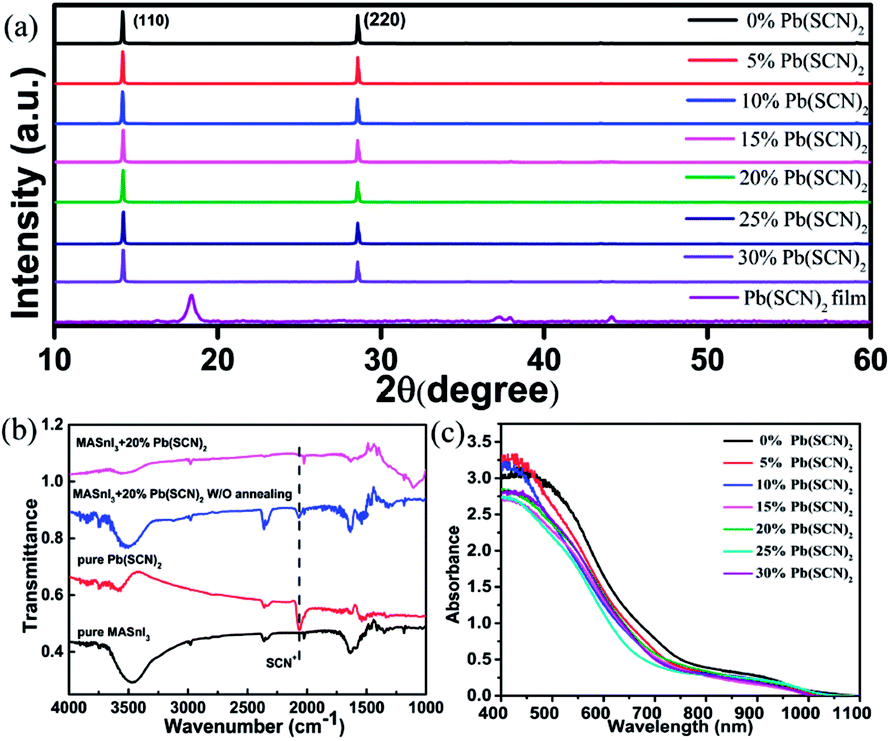 | ||
| Fig. 3 (a) XRD patterns of a Pb(SCN)2 film and the MASnI3 films with various concentrations of Pb(SCN)2 additive in the precursors. (b) FTIR spectra of the films of Pb(SCN)2, MASnI3 and MASnI3 with 20% Pb(SCN)2 additive with and without annealing. (c) Absorbance spectra of the MASnI3 films with various concentrations of Pb(SCN)2 additives in the precursors. | ||
 | ||
| Fig. 4 Top-view SEM images of the MASnI3 films with 20% Pb(SCN)2 additive (a). SEM-EDS elemental mappings of Sn (green) (b), Pb (red) (c), and I (yellow) (d) for the MASnI3 film. | ||
The excess PbI2 can reduce the absorbance of the perovskite films as shown in Fig. 3c, which would result in a decrease in Jsc. In order to further understand the effects of Pb(SCN)2 on the MASnI3 thin films, the photoluminescence (PL) spectra of the films developed from the precursor solutions with different Pb(SCN)2 concentrations have been measured, as shown in Fig. S8.† The PL intensity is enhanced with the increasing amount of Pb(SCN)2, thus, we speculate that the grain boundaries (GBs) in the perovskite films may be passivated by the excess PbI2 at the GBs and which can exhibit beneficial effects on the cell performance, as reported by others.26
We fabricated planar heterojunction photovoltaic devices employing the Sn-based perovskites as active layers. Fig. 5a indicates the inverted device structure adopted in this work.
 | ||
| Fig. 5 (a) Schematic of the device structure of the solar cells. (b) J–V curves of the cells prepared using MASnI3 with various concentrations of Pb(SCN)2 additives in the precursors, measured under forward voltage scanning. Steady-state efficiencies and current densities of the devices using MASnI3 without (c) and with 20% Pb(SCN)2 (d) at constant bias voltages of 0.18 V and 0.41 V, respectively. | ||
The effects of the concentration of Pb(SCN)2 additive on the device performance of the Sn-based PSCs have been investigated. Fig. 5b shows the J–V curves for the PSCs prepared with different concentrations of Pb(SCN)2 under forward voltage scanning. The best performance has been acquired in the devices with MASnI3 prepared from the precursor solution with 20% Pb(SCN)2. The Jsc begins to decline when the amount of Pb(SCN)2 is more than 20%. The reduction of Jsc is related with the decline of the absorbance of the perovskite films, and that enables the cells with a low Jsc. Besides, the Pb ions can lower the LUMO level of Sn–I perovskite materials and increase the open circuit voltage of solar cells.27–33 As shown in Table S1 (ESI†), the FF of the device also gains an obvious improvement with the addition of Pb(SCN)2. The high FF value can be ascribed to suppressed defect-mediated carrier recombination, as well as balanced carrier transport.34,35 The cell with the perovskite absorber from the precursor solution without Pb(SCN)2 only achieves a PCE of 0.87% with a Jsc of 5.37 mA cm−2, an Voc of 0.30 V, and a FF of 54%. The cell using the perovskite absorber with 20% Pb(SCN)2 in the precursor realizes a PCE 5.69% with a Jsc of 17.69 mA cm−2, an Voc of 0.50 V, and a FF of 64%, revealing significantly improved FF and PCE. Fig. S9† shows the J–V curves under reverse voltage scanning, and we can find that the Voc is still on the rise while the Jsc reaches its maximum value as the amount of Pb(SCN)2 reaches 20%. This is basically consistent with the law of J–V curves under forward voltage scanning. The J–V curves of the PSCs with 20% Pb(SCN)2 added in the perovskite precursor with the vacuum-assisted annealing (VAA) and without vacuum treatment were also tested. The film without vacuum treatment has an increased surface roughness, and makes the coverage is not complete, so these lead to the increase of the leakage current and the decrease of the fill factor, as shown in Fig. S10.† Therefore, the results prove that the vacuum-assisted annealing (VAA) is indeed an effective method to improve the device performance.
Fig. 5c and d show the steady-state efficiencies and current densities of the solar cells without and with 20% Pb(SCN)2 additive in the precursors under the standard illumination of AM 1.5 G. From the figures, one can find that the addition of Pb(SCN)2 cannot improve the stability, but enhances significantly the efficiency of the Sn-perovskite solar cells. The performance of the devices in the air without encapsulation have been tracked. As shown in Fig. S11,† the PCE of the MASnI3 PSCs decays to 11% of its original value within 10 min, while the PCE of the perovskites PSC fabricated by the solution with 20% Pb(SCN)2 retains 50% of its original value for over 100 min. The reason for the fast degradation of the MASnI3 PSCs could be attributed to the fast oxidation of MASnI3 under the presence of oxygen and moisture in the air. However, the compact morphology of 20% Pb(SCN)2 perovskites PSCs slows down this oxidation process, which results in a more stable device performance.
Fig. 6a shows the external quantum efficiency (EQE) spectra of the cells using perovskite absorbers prepared with 0, 10%, 20%, 30% Pb(SCN)2 additive in the precursors. The devices with a higher amount of Pb(SCN)2 exhibit larger EQE. The reduction of the defects makes it more capable of collecting charge but it will severely affect the absorption when the lead content is further increased to 30%. The J–V curves of the maximum PCE cell with 20% Pb(SCN)2 are shown in Fig. S13.† The photovoltaic parameters were measured under both reverse and forward voltage scanning, as shown in Table S2. Fig. S14† shows the EQE spectra of the maximum PCE cells using the perovskite absorbers with 20% Pb(SCN)2 additive in the precursor. The integrated current densities based on these curves are 16.15 mA cm−2 for the cells using perovskite absorbers with 20% Pb(SCN)2 in the precursors.
 | ||
| Fig. 6 (a) External quantum efficiency (EQE) spectra of the solar cells based on MASnI3 with various concentrations of Pb(SCN)2 additives in the precursors. (b) Open circuit voltage (VOC) of the perovskite PSCs with 20% Pb(SCN)2 additive plotted against incident light intensity. (c) The differences values of the ideality factor n of the Sn perovskite-based PSCs with different Pb(SCN)2 concentration. (d) Transient photocurrent (TPC) response of the solar cells using MASnI3 with different Pb(SCN)2 concentrations. | ||
To further clarify the charge recombination processes in the Sn-based PSCs, the light-intensity-dependent characterization was investigated. The light-intensity-dependent VOC provides critical insights into the mechanism of the recombination processes in the PSC devices. The relationship between VOC and light intensity can be expressed as:
 | (1) |
Conclusions
We have demonstrated that a small amount of Pb(SCN)2 additive in the perovskite precursors can retard the crystallization rate of the MASnI3 films during solution deposition, which results in a significant reduction in the pinholes and an obvious improvement in the morphology of the Sn-perovskite films. SCN ions are volatilized in the post annealing of the films, and Pb ions form PbI2 in the MAPbSnI3 particles. The existing of PbI2 not only passivates the Sn-perovskite particles but also benefits performance enhancement. The PSCs based on the MASnI3 film with 20% Pb(SCN)2 additive achieves a maximum PCE of 6.03%, a Jsc of 17.03 mA cm−2, an VOC of 0.54 V, and a FF of 66%.Experimental
Device fabrication
Methylammonium iodide (CH3NH3I), PEDOT:PSS (Clevious P VP AI 4083), SnI2 (99.999%), PCBM (99.9%), PEI(99.9%), and Al (99.99%) were purchased from H. C. Stark Company, Alfa Aesar, Puyang Yongxin Fullerene Technology Co., Ltd, Xi'an Polymer Light Technology Corp, sigma and China New Metal, respectively. The ITO-coated glass substrates were cleaned successively with detergent, deionized water, and isopropyl alcohol in an ultrasonic bath for 30 min, respectively, and then treated with oxygen plasma for 15 min. PEDOT:PSS aqueous solution was filtered through a 0.45 μm filter and spin coated on the ITO surface at 3000 rpm for 40 s and then annealed at 140 °C for 15 min, forming a hole transport layer. The perovskite films without Pb(SCN)2 in the precursors were prepared by spin coating the precursor solutions consisting of 186.3 mg of SnI2 and 79.5 mg of MAI dissolved in 464 μL of N,N-dimethylformamide and 36 μL of dimethyl sulfoxide. The molar ratio between SnI2 and MAI is 1:1. The perovskite films with 5%, 10%, 15%, 20%, 25% and 30% Pb(SCN)2 (Sigma, 99.5%) in the precursors were prepared by spin coating the solutions with Pb(SCN)2. All the perovskite precursors with and without Pb(SCN)2 were stored at 70 °C and stirred overnight in a glove box. The following procedures for the fabrication of the solar cells were performed in a nitrogen-purged glove box. A PEDOT:PSS layer was then spin-coated onto the ITO substrates at 4000 rpm for 60 s and dried at 140 °C for 20 min. The coated substrates were then transferred to a nitrogen-filled glove-box. The perovskite layer was spin-coated on the PEDOT:PSS substrate at 5000 rpm for 20 s. The mixed solvent of toluene:chloroform (7:3 in volume) was used as the antisolvent during the spin-coating process. Then the perovskite film was placed in a vacuum cover and a mechanical pump was employed to keep the working pressure inside the cover at 1.325 kPa. After 10 minutes the perovskite film was annealed at 100 °C for 10 minutes in the vacuum cover. After the fabrication of perovskite layer, PCBM was spin-cast at 2000 rpm for 60 s from a 20 mg mL−1 chlorobenzene solution. Then PEI was spin-cast at 3000 rpm for 60 s from a 0.1 wt% isopropanol. Finally, Al (90 nm) was deposited through a mask via thermal evaporation at a rate of 0.2–1.0 Å s−1 to produce 0.045 cm2 pixels.
Film and device characterization
The XRD patterns were detected with a Bruker D8 Advance X-ray diffraction meter. The absorption spectra of the photoactive perovskite films coated on the ITO substrates were measured by an ultraviolet visible (UV-Vis) absorption spectrophotometer (Shimadzu UV-3101PC). The morphologies and the elemental mappings energy dispersive spectrometer (EM-EDS) of the perovskite films were investigated using a scanning electron microscope (SEM, Hitachi S-4800) with an accelerating voltage of 15 kV. The photoluminescence (PL) spectra of the perovskite films were measured by a fluorescence spectrophotometer. Fourier Transform Infrared (TRPL) spectra were performed by a square-pulsed optical excitation which was generated from a light emitting diode (LED) driven by a function generator, and a 50 Ω input termination of the oscilloscope was used. The current density–voltage (J–V) curves of the inverted PSCs were measured by a Keithley 6430 Source Measure Unit under nitrogen and a Mass 1.5 G illumination at 100 mW cm−1−2 (SAN-EI Electric, XEC-301S). The incident photon-to-current efficiency (IPCE) was performed using a solar cell QE/IPCE measurement system (Zolix Solar Cell Scan 100). The light intensity dependent photo voltage (LIPV) was conducted using an array of 12 focused cool white LEDs of 1 W. The stability test was carried out in air with 50% humidity. The light intensity of the LEDs was detected by a corrected Si photodiode, and the electrical input power of the LEDs was adjusted with a controlled power supply to change the illumination intensities ranging from 5 to 500 mW cm−2. The values of the open-circuit voltage (Voc) and the short-circuit current density (Jsc) were collected by a 16 bit data acquisition board (NI-6052E) with an input impedance of 10 MΩ and 50 Ω at room temperature, respectively. In order to reach a steady-state condition, the time of the data acquisition was chosen to be 100 ms through the measurement process. The transient photocurrent (TPC) measurement was conducted using a signal generator with a voltage signal of 200 μs and 50 Hz as a power supply of the white LEDs that produced pulsed light. The device was connected with a resistor of 50 Ω in series and the voltage applied to the resistor was collected by the oscilloscope and the TPC was calculated simply by the voltage divided by the resistance.Conflicts of interest
There are no conflicts to declare.Acknowledgements
This work was supported by the Natural Science Foundation of China (Grant No. 61475017)Notes and references
- A. Kojima, K. Teshima and Y. Shirai, et al., J. Am. Chem. Soc., 2009, 131(17), 6050–6051 CrossRef CAS PubMed.
- H. S. Kim, C. R. Lee and J. H. Im, et al., Sci. Rep., 2012, 2, 591 CrossRef PubMed.
- N. G. Park, J. Phys. Chem. Lett., 2013, 4(15), 2423–2429 CrossRef CAS.
- W. S. Yang, J. H. Noh and N. J. Jeon, et al., Science, 2015, 348(6240), 1234–1237 CrossRef CAS PubMed.
- M. M. Lee, J. Teuscher and T. Miyasaka, et al., Science, 2012, 338(6107), 643–647 CrossRef CAS PubMed.
- M. Liu, M. B. Johnston and H. J. Snaith, Nature, 2013, 501, 395 CrossRef CAS PubMed.
- H. Zhou, Q. Chen and G. Li, et al., Science, 2014, 345(6196), 542–546 CrossRef CAS PubMed.
- D. Bi, W. Tress and M. I. Dar, et al., Sci. Adv., 2016, 2(1), e1501170 Search PubMed.
- W. Chen, Y. Wu and Y. Yue, et al., Science, 2015, 350(6263), 944–948 CrossRef CAS PubMed.
- D. P. McMeekin, G. Sadoughi and W. Rehman, et al., Science, 2016, 351(6269), 151–155 CrossRef CAS PubMed.
- Q. Wang, Q. Dong and T. Li, et al., Adv. Mater., 2016, 28(31), 6734–6739 CrossRef CAS PubMed.
- C. C. Stoumpos and M. G. Kanatzidis, Halide Perovskites:, Adv. Mater., 2016, 28(28), 5778–5793 CrossRef CAS PubMed.
- D. Bi, P. Gao and R. Scopelliti, et al., Adv. Mater., 2016, 28(15), 2910–2915 CrossRef CAS PubMed.
- NREL, Best Research-Cell Efficiencies, https://www.nrel. Gov/pv/assets/images/efficiency-chart.png, (accessed: April 2017).
- N. K. Noel, S. D. Stranks and A. Abate, et al., Energy Environ. Sci., 2014, 7(9), 3061–3068 CAS.
- F. Hao, C. C. Stoumpos and R. P. H. Chang, et al., J. Am. Chem. Soc., 2014, 136(22), 8094–8099 CrossRef CAS PubMed.
- (a) S. Rühle, Sol. Energy, 2016, 130, 139–147 CrossRef; (b) Z. Yang, A. Rajagopal, C. C. Chueh, S. B. Jo, B. Liu, T. Zhao and A. K. Jen, Adv. Mater., 2016, 28, 8990 CrossRef CAS PubMed.
- M. H. Kumar, et al., Adv. Mater., 2014, 26(41), 7122–7127 CrossRef CAS PubMed.
- F. Hao, et al., J. Am. Chem. Soc., 2015, 137(35), 11445–11452 CrossRef CAS PubMed.
- F. Hao, et al., Nat. Photonics, 2014, 8(6), 489–494 CrossRef CAS.
- F. Zuo, S. T. Williams and P. W. Liang, et al., Adv. Mater., 2014, 26(37), 6454–6460 CrossRef CAS PubMed.
- W. Liao, D. Zhao, Y. Yu, N. Shrestha, K. Ghimire, C. R. Grice, C. Wang, Y. Xiao, A. J. Cimaroli, R. J. Ellingson, N. J. Podraza, K. Zhu, R.-G. Xiong and Y. Yan, J. Am. Chem. Soc., 2016, 138, 12360 CrossRef CAS PubMed.
- T. Yokoyama, et al., J. Phys. Chem. Lett., 2016, 7(5), 776–782 CrossRef CAS PubMed.
- C. Roldan-Carmona, P. Gratia and I. Zimmermann, et al., Energy Environ. Sci., 2015, 8(12), 3550–3556 CAS.
- H. Dong, Z. Wu, J. Xi, X. Xu, L. Zuo, T. Lei and A. K. Y. Jen, Adv. Funct. Mater., 2018, 28(2), 1870013 CrossRef.
- X. Li, F. Hao and X. Zhao, et al., ACS Appl. Mater. Interfaces, 2017, 9(40), 34833–34843 CAS.
- Y. Takahashi, et al., Dalton Trans., 2011, 40(20), 5563–5568 RSC.
- D. Zhao, et al., Nat. Energy, 2017, 2, 17018 CrossRef CAS.
- F. Hao, et al., J. Am. Chem. Soc., 2014, 136(20), 8094–8099 CrossRef CAS PubMed.
- Y. Li, et al., Adv. Energy Mater., 2016, 6(20) Search PubMed.
- Y. Ogomi, et al., J. Phys. Chem. Lett., 2014, 5(20), 1004–1011 CrossRef CAS PubMed.
- L. Zhu, et al., Nanoscale, 2016, 8(20), 7621–7630 RSC.
- F. Zuo, et al., Adv. Mater., 2014, 26(20), 6454–6460 CrossRef CAS PubMed.
- D. Bi, W. Tress, M. I. Dar, P. Gao, J. Luo, C. Renevier, K. Schenk, A. Abate, F. Giordano, J.-P. C. Baena, J.-D. Decoppet, M. Gratzel and A. Hagfeldt, et al., Sci. Adv., 2016, 2, e1501170 Search PubMed.
- M. Zhang, M. Lyu, J.-H. Yun, M. Noori, X. Zhou, N. A. Cooling, Q. Wang, H. Yu, P. C. Dastoor and L. Wang, Nano Res., 2016, 9, 1570–1577 CrossRef CAS.
- B. Zhao, M. Abdi-Jalebi and M. Tabachnyk, et al., Adv. Mater., 2017, 29(2), 1604744 CrossRef PubMed.
- X. Huang, L. Lv and Y. Hu, et al., Org. Electron., 2017, 42, 107–114 CrossRef CAS.
- L. J. A. Koster, V. D. Mihailetchi and R. Ramaker, et al., Appl. Phys. Lett., 2005, 86(12), 123509 CrossRef.
- D. Zhao, M. Sexton and H. Y. Park, et al., Adv. Energy Mater., 2015, 5(6), 1401855 CrossRef.
- J. C. Blancon, W. Nie and A. J. Neukirch, et al., Adv. Funct. Mater., 2016, 26(24), 4283–4292 CrossRef CAS.
- N. Marinova, W. Tress and R. Humphry-Baker, et al., ACS Nano, 2015, 9(4), 4200–4209 CrossRef CAS PubMed.
- L. Longfeng, et al., Chem. Mater., 2014, 27(1), 44–52 Search PubMed.
Footnotes |
| † Electronic supplementary information (ESI) available. See DOI: 10.1039/c8ra00809d |
| ‡ These authors contributed equally to this work. |
| This journal is © The Royal Society of Chemistry 2018 |