DOI:
10.1039/C8RA00716K
(Paper)
RSC Adv., 2018,
8, 10064-10071
Hexagonal VO2 particles: synthesis, mechanism and thermochromic properties†
Received
24th January 2018
, Accepted 6th March 2018
First published on 12th March 2018
1. Introduction
Vanadium dioxide (VO2) possesses several phases, M, R, B,1 A,2 and D,3 and exhibits fantastic phase transition between them.4,5 The distinguishing feature of each polymorph is the arrangement scheme of edge- or corner-sharing VO6 octahedra. Monoclinic VO2 (M) shows a reversible first-order metal-insulator transition (MIT) at 68 °C.6 When the insulating VO2 (M) is converted into the metallic rutile phase (R), drastic changes occur in both electrical and optical properties.7,8 As a result, VO2 has been attracting much attention owing to the potential applications in high-tech fields, such as, sensors,9,10 catalysts,11 lithium-ion batteries,12 storage medium,13 smart windows14–17 and so on. Since the size and morphology of nanostructures affect the physical and chemical properties greatly. Therefore, it is very important to understand the formation and growth behavior of VO2 and make it controllable.
A variety of physical and chemical strategies, such as, atomic layer deposition,18 sol–gel,19 ion implantation technique,20 chemical vapor deposition,21 pulsed laser deposition,22 magnetron sputtering23,24 and solution-based synthesis25 have been developed to fabricate VO2 nanostructures. Among them, the solution-based method gained increasing attention because of the simple preparation process and low cost. In the solution-based synthesis, VO2 nanostructures of different phases and morphologies have been produced, dependent on the reaction temperature (Fig. S1†), reaction time, precursor concentration and autoclave filling ratio. Hexagonal VO2 (M) was obtained by the hydrothermal synthesis and, VO2 (B), VO2 (A) and VO2 (D) phases appeared as intermediates. To be confused, different intermediates were involved in the hydrothermal process. VO2 (B) is firstly transformed into VO2 (A) and then into VO2 (R).26 However, VO2 (A) does not appear in some cases.15 Here, it is demonstrated that the hydrothermal reaction process is closely related to the reaction speed that is easily controlled by changing the concentration of precursor solutions. Hexagonal structure has been evidenced extensively, but the formation mechanism is still ambiguous. Cao et al.27 proposed that it could be ascribed to the similar growth rate along the six low-energy (20![[1 with combining macron]](https://www.rsc.org/images/entities/char_0031_0304.gif) ) facets, while someone suggested that it was assembled from nanobelts. In this paper, the coherent relationship between each branches of hexagonal structure is characterized, which provides deep insights into the morphology evolution of VO2 (M).
) facets, while someone suggested that it was assembled from nanobelts. In this paper, the coherent relationship between each branches of hexagonal structure is characterized, which provides deep insights into the morphology evolution of VO2 (M).
2. Experimental details
VO2 nanostructures were synthesized by the hydrothermal method using V2O5 as the vanadium source and oxalic acid (H2C2O4) as a reducing agent. The filling ratio of the vessel is about 70%. Firstly, oxalic acid (H2C2O4) and V2O5 (1![[thin space (1/6-em)]](https://www.rsc.org/images/entities/char_2009.gif) :1–1:3 in molar) are directly added into 35 ml deionized water at room temperature (RT), and then ammonium tungstate ((NH4)10W12O41·xH2O) is dispersed into the above solution and stirred for 4 hours. 35 ml of the precursor solution is transferred into a 50 ml stainless autoclave with a Teflon liner and ultimately the autoclave is heated up to 260 °C for 1–24 h and then cooled in air to room temperature. The resulting black precipitate is collected and washed with distilled water and ethanol three times by centrifugation and then dried in vacuum at 60 °C for 12 h. The as-prepared VO2 nanostructures are ultrasonically dispersed in deionized water for 30 min, and an appropriate quantity of silane coupling agent KH-570 is added with ultrasonic treatment for another 30 min. Then, polyurethane (PU, DISPERCOLLU54, Bayer) is added with magnetic stirring for 10 min. Finally, the suspension is uniformly cast onto a polyethylene terephthalate (PET) substrate using an automatic coating machine and dried at 80 °C for 1 min.30
:1–1:3 in molar) are directly added into 35 ml deionized water at room temperature (RT), and then ammonium tungstate ((NH4)10W12O41·xH2O) is dispersed into the above solution and stirred for 4 hours. 35 ml of the precursor solution is transferred into a 50 ml stainless autoclave with a Teflon liner and ultimately the autoclave is heated up to 260 °C for 1–24 h and then cooled in air to room temperature. The resulting black precipitate is collected and washed with distilled water and ethanol three times by centrifugation and then dried in vacuum at 60 °C for 12 h. The as-prepared VO2 nanostructures are ultrasonically dispersed in deionized water for 30 min, and an appropriate quantity of silane coupling agent KH-570 is added with ultrasonic treatment for another 30 min. Then, polyurethane (PU, DISPERCOLLU54, Bayer) is added with magnetic stirring for 10 min. Finally, the suspension is uniformly cast onto a polyethylene terephthalate (PET) substrate using an automatic coating machine and dried at 80 °C for 1 min.30
The morphology of VO2 nanostructures were characterized by transmission electron microscopy (TEM) and field-emission scanning electron microscopy (FESEM, JSM-7000F). The crystal phases was determined by X-ray diffraction (GIXRD, Shimadzu XRD-7000) with Cu Kα radiation (λ = 0.154 nm) at a fixed incident angle of 0.5° and 2θ scanning rate of 8° min−1. Differential scanning calorimetry (DSC, DSC204F1, NETZSCH, Germany) were measured at 50–100 °C with a heating rate of 5 °C min−1 under a nitrogen flow. The elemental component and chemical valence states were determined by X-ray photoelectron spectroscopy (Thermo Scientific K-Alpha, XPS). The transmittance spectra were measured in the range of 300–2200 nm at normal incidence using a Hitachi U-4100 spectrometer.
3. Results and discussion
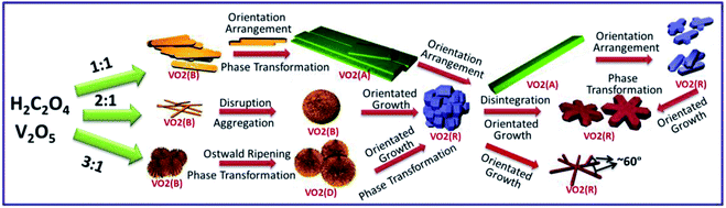
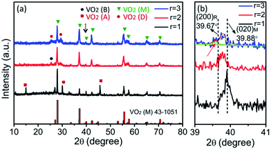
Fig. 1 shows the XRD patterns of the samples prepared at three molar ratios (r = 1, 2, 3) of H2C2O4 to V2O5. Different phase evolutions, VO2 (B) → VO2 (A) → VO2 (M), VO2 (B) → VO2 (M) and VO2 (B) → VO2 (D) → VO2 (M) are evidenced. As shown in Fig. 1a, at the reaction condition of r = 1, only the diffraction peaks of VO2 (B) are identified for 1 h hydrothermal reaction. The corresponding SEM image is shown in Fig. 2a, VO2 (B) exists in the form of nanobelts with 2–4 μm long and 200–400 nm wide. The VO2 (B) phase is confirmed by the TEM images in Fig. 3. The HRTEM image in Fig. 3b shows the lattice fringe spacing of 0.353 nm, corresponding to (110) lattice plane of monoclinic VO2 (B). As illustrated by the selected area electron diffraction (SAED) pattern in the inset of Fig. 3a, the zone axis of the reciprocal lattice is [001]. If the hydrothermal reaction time is elongated to 6 h, new diffraction peaks corresponding to VO2 (A) and VO2 (M) phases appear on the XRD pattern, and a great number of nanobelts with rectangular ends emerge28 (Fig. 2b). If the reaction time is further elongated to 12 h, the peaks of VO2 (B) vanish completely and the peak intensity of VO2 (A) and VO2 (M) increases greatly. As displayed in Fig. 2c, rectangular nanobelts and truncated nanorods coexist. Fig. 3d presents the HRTEM image of the rectangular nanobelts in Fig. 3c, the fringe spacing of 0.59 nm matches well with the (110) plane of tetragonal VO2 (A). According to the SEM images in Fig. 2b–d and the XRD patterns in Fig. 1a, it can be concluded that the truncated nanorods should be VO2 (M). If the reaction time is elongated to 24 h, the peaks of VO2 (A) become weakened gradually, but those of VO2 (M) are enhanced, that is, the growth of VO2 (M) rather than VO2 (A) dominates after the elimination of VO2 (B). At the reaction condition of r = 2, no peak of VO2 (A) appears on the XRD pattern in Fig. 1b, and the size of VO2 (B) nanostructure (Fig. 2e) is reduced substantially as compared to that in Fig. 2a. Phase transition between VO2 (B) and VO2 (R) was studied in situ by electron microscopy,29 and it was found that VO6 octahedra (Fig. S2†) in VO2 (B) abruptly broke into nanocrystallites and half of VO6 octahedra reorient into rutile structure. VO2 (B) in spheroidal morphology appears (Fig. 2g) because of severe agglomeration. At the reaction condition of r = 3, VO2 (B) with nanorod-like or nanobelt-like morphology (Fig. 1c) aggregate into urchin-like structures to minimize the energy.30 Further growth leads to the formation of larger sphere-like particles as a result of Ostwald ripening (Fig. 2j). If the hydrothermal reaction time is elongated, oriented growth plays a dominant role gradually, resulting in hexagonal structure.31 According to the XRD pattern in Fig. 1c and SEM images in Fig. 2j–k, the particles are indeed VO2 (D) phase. The lattice fringes with a spacing of 0.372 nm corresponds to the (011) lattice plane of VO2 (D), as shown in Fig. 3f. If the ratio of H2C2O4:V2O5 is lower than 1 or higher than 3, no VO2 (M) appears. However, pure VO2 (A) is obtained when r is slightly lower than 1 (Fig. S3†). Cao et al. prepared W-doped hexagonal VO2 (M) via one-step hydrothermal reactions at 240 °C for 7 days, and proposed that the hexagonal morphology was assembled by the VO2 (M) rods along six low-index planes,32 but they did not provide us the underlying mechanism for the formation of the hexagonal morphology. Ji et al. thought that the transformation from VO2 (A) to VO2 (M) was a resolving and re-crystallization process, and the hexagonal particles could be attributed to the electrostatic attraction.33 However, in this work, no agglomeration and melting behavior are observed during the transformation from VO2 (A) into VO2 (M), but the ultra-long VO2 (A) belts are broken into truncated VO2 (M) rods, and hexagonal morphology of VO2 (M) is formed through an epitaxial growth taking the center regions of rods as the nucleation sites [Fig. 2c and d].
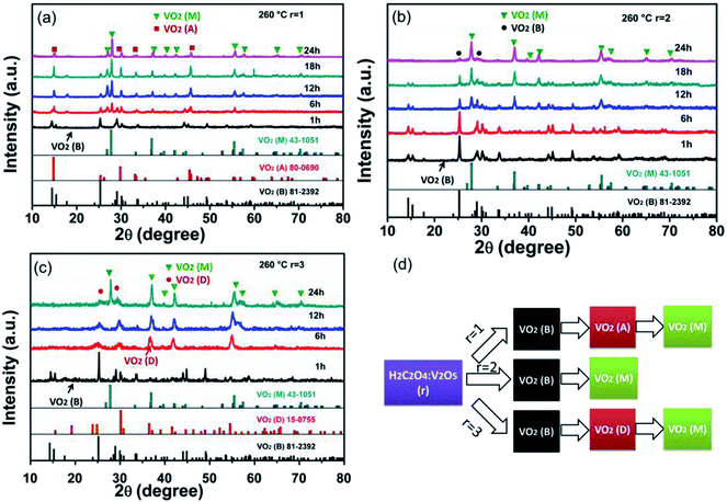 |
| | Fig. 1 XRD patterns of samples synthesized at 260 °C with different r (H2C2O4:V2O5): (a) r = 1, (b) r = 2 and (c) r = 3; (d) the diagram of phase evolution. | |
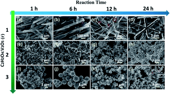 |
| | Fig. 2 SEM images of samples prepared at 260 °C under the condition of r (H2C2O4:V2O5) = 1: (a) 1 h, (b) 6 h, (c) 12 h, (d) 24 h; r = 2: (e) 1 h, (f) 6 h, (g) 12 h, (h) 24 h; r = 3: (i) 1 h, (j) 6 h, (k) 12 h, (l) 24 h. | |
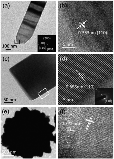 |
| | Fig. 3 (a), (c) and (e) low-resolution TEM image of VO2 (B), VO2 (A) and VO2 (D), respectively. (b), (d) and (f) corresponding to the HRTEM images. | |
Fig. 4 presents the TEM images of VO2 nanostructure with hexagonal morphology. The lattice spacings of 0.242, 0.230 and 0.242 nm in Fig. 4b correspond to (2), (020) and (21) planes of VO2 (M), respectively. The SAED pattern from an individual nanorod (Fig. 4d) is indexed to monoclinic VO2 with a zone axis of [102]. The diffraction pattern does not change as the electron beam is moved along the nanobelt, characteristic of single-crystal feature. The experimental result is well consistent with the calculated SAED pattern in Fig. 4d. The SAED pattern shows that the growth is along [100] direction. As depicted in Fig. 4e, bud-like nanoparticles grow outwards from a nanorod, in which (21)1//(2)2 and (2)1//(020)2 coherent interface exist in the adjacent branches, thus small lattice distortions emerge if they are combined into a heterogeneous interface. It is demonstrated that the angle (about 60°) between the adjacent branches is decided by the coherent interfaces. The overlapped FFT patterns in Fig. 4g confirm the coherent crystalline planes between the adjacent branches, and Fig. 4h schematically shows the atomic arrangement.
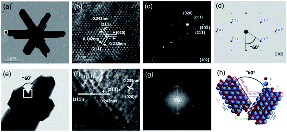 |
| | Fig. 4 (a) Low-magnification TEM images, (b) HRTEM image at the VO2 rod end, (c) SAED pattern of the particle in (b) and (d) the calculated SAED pattern from [102] zone axis, (e) low-magnification TEM image, (f) HRTEM image of the overlap region between adjacent branches, (g) the FFT pattern of the overlap region from panel (f) and (h) the atomic arrangement in panel (f). | |
Fig. 5 schematically shows the evolution of VO2 (M) hexagonal morphology. The reaction proceeds toward the lowest energy, and promotes the oriented attachment.34 Firstly, V2O5 is reduced by H2C2O4 and the interphase VO2 (B) is produced. As the reaction proceeds, oriented attachment or aggregation occurs spontaneously in order to minimize energy,35 thus a great number of belts (Fig. 2b) or urchin-like (Fig. 2i) structure appear. Then metastable VO2 (B) transforms into a more stable phase gradually. As aforementioned, different growth processes yield different interphases, which are dominated by nucleation rate and growth rate. H2C2O4 plays an important role in reduction rate and further affects the supersaturation. The ratio of growth rate to nucleation rate is high under low supersaturation condition and vice versa (Fig. S4†). In another word, the competition between nucleation rate and growth rate results in different morphologies, high nucleation rate results in aggregation and high growth rate leads to ultra-long nanobelts. VO2 (A) is from the stack of VO2 (B) nanobelts. At high nucleation rate, VO2 (B) prefers to aggregation rather than stacking,36,37 and thus no VO2 (A) appears. Hydrothermal reaction condition of r = 1 (Fig. 2d) yields large hexagonal structure with ultra-long branches in the range of 4–8 μm and 600 nm in width. The length decreases to 4–6 μm (r = 2) and 2–4 μm (r = 3) respectively with increasing H2C2O4. VO6 octahedra of VO2 (B) is different from VO2 (R), but similar to VO2 (A) (Fig. S2†). Thus, more energy is needed for the transformation from VO2 (B) to VO2 (R) (r = 2) than to VO2 (A) (r = 1). So an appropriate H2C2O4 could promote the formation of VO2 (R).
 |
| | Fig. 5 Schematic evolution of the polymorph morphology. | |
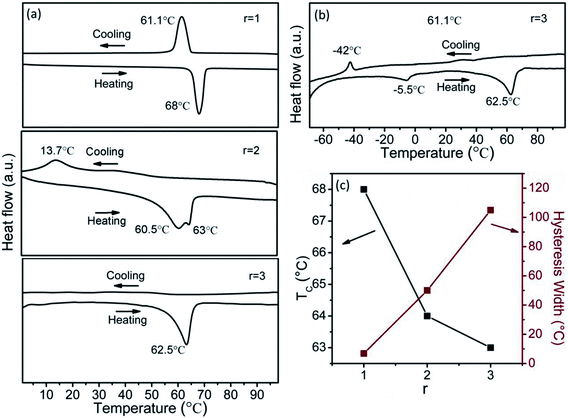
Fig. 6a shows the DSC curves of the as-synthesized VO2 (M) with r of 1, 2 and 3. The DSC curves of both r = 1 and 2 display endothermic and exothermic profiles upon heating and cooling in the temperature range of 0–100 °C, indicating a reversible phase transition,38 but only an endothermic profile is observed in the heating process for r of 3. So the temperature range from −70 to 100 °C was adopted for the DSC measurement for r of 3, and the results are displayed in Fig. 6b. The phase transition temperature and hysteresis width of the samples are summarized in Fig. 6c. Apparently, the samples exhibit dramatically different phase transition properties. The TC is 68, 60.5 and 62.5 °C during heating process, and 61.1, 137 and −42 °C during cooling process. The hysteresis width is about 6.9, 48.6 and 104.5 °C for the as-synthesized VO2 (M) particles obtained at r = 1, 2, 3, respectively, and the hysteresis width is not dependent on the particle size of micrometers. As shown in Fig. 7a, some residual VO2 (A), VO2 (B) and VO2 (D) phases exist except the dominating VO2 (M) phase at r = 1, 2 and 3, respectively. The residual VO2 (A) has little effect on the phase transition of VO2 (M) obtained under r = 1, as shown in Fig. 6c. On the contrary, the phase evolution of VO2 (M) obtained under r = 2, 3 is indeed a recrystallization process, and thus there is a considerable interaction between VO2 (B) and VO2 (M) as well as between VO2 (D) and VO2 (M), so the residual VO2 (B) and VO2 (D) affect the phase transition of VO2 (M) obtained under r = 2 and 3. The transformation from monoclinic (020)M plane at room temperature to (200)R plane at high temperature was accompanied by the peak shift from 39.88° to 39.67°. As shown in Fig. 7b, the peak of (020)M plane shifts toward the smaller angle at r = 2 and 3. In addition, a new peak appears at 39.5° for the sample prepared under r = 3, and it is lower than 39.67°, implying increased V–V bond length and stabilized VO2 (R) at room temperature.39 Therefore, more energy is needed to induce the phase transition in the cooling cycle, resulting in the large hysteresis width. Fig. 9a and b show the optical transmittance of the as-synthesized and annealed samples, respectively. All the samples show a sharp optical contrast in near infrared at 20 and 90 °C. The Tvis and ΔT2000 obtained from Fig. 9a and b are displayed in Fig. 9c and d, respectively. Tvis changes a little but ΔT2000 increases significantly upon thermal annealing. It means that the residual phases affect the NIR modulation ability of VO2 (M) considerably.
 |
| | Fig. 6 (a and b) DSC curves of the as-prepared samples, (c) TC and hysteresis width. | |
 |
| | Fig. 7 (a) XRD patterns of as-prepared samples with r of 1–3, (b) magnified patterns. | |
 |
| | Fig. 8 (a) XRD patterns of the annealed samples (b) DSC curves of the annealed samples. | |
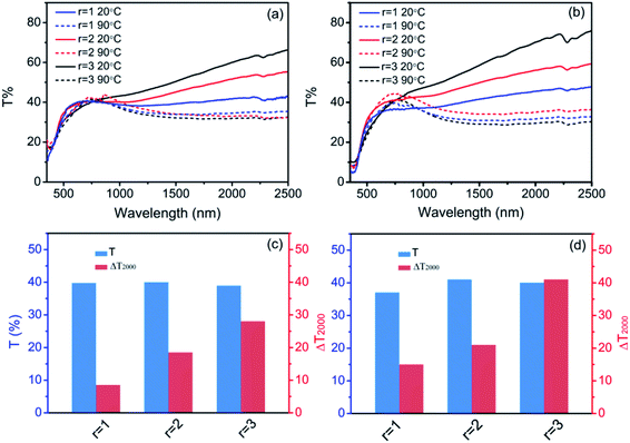 |
| | Fig. 9 Optical transmittance spectra of the (a) as-prepared and (b) annealed samples, (c and d) Tvis and ΔT2000 of the as-prepared and annealed samples, respectively. | |
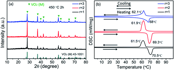
It is difficult to obtain pure VO2 (M) in a V2O5–H2C2O4 reaction system if no thermal annealing or doping is done.37 As shown in Fig. 8a, pure VO2 (M) is obtained after thermal annealing at 450 °C for 2 h. The TC is about 70.5, 69.3 and 68 °C during the heating process, and 61.5, 61.9 and 62.1 °C during cooling process (Fig. 8b), and the hysteresis width is about 9, 7.4 and 5.9 °C when r is 1, 2 and 3, respectively. Apparently, the hysteresis widths of the samples prepared at r = 2, 3 are reduced dramatically upon thermal annealing. But the particle size and structure changes little [Fig. S5†], indicating high stability of the hexagonal VO2 (M). As stated above, the intermediate phases indeed have a great influence on the hysteresis width. In addition, the hysteresis width of the pure VO2 (M) obtained here is significantly smaller than what was reported.25,40 It can be due to the lattice distortions in coherent interface of adjacent branches. The defects act as nucleation site for metal-insulator transition and decrease the driving force. The number of branch grows as increasing r, as shown in Fig. 2, and the smallest hysteresis is obtained at r of 3.
Based on the preparation process in Fig. S6,† the composite films are prepared to measure the optical properties. The suspension composed of VO2 (M) particles is uniformly cast on the PET substrate and the film exhibits a canary yellow color (Fig. S3b†). Fig. 9a and b show the optical transmittance of the samples before and after annealing, respectively. All the samples show a sharp optical contrast in near infrared at 20 and 90 °C, indicating that the phase transition occurs. In addition, ΔT2000 is continuously improved from 28.3% to 41% as r increases from 1 to 3, due to the reduced sizes of the particles.
Tungsten (W) is the most effective dopant for reducing the phase transition temperature. Fig. 10a shows a wide-range survey X-ray photoelectron spectroscopy (XPS) of W-doped VO2 (M). C, V, W and O are detected, in which the signal of C is from the contamination on surface. From Fig. 10b, it can be seen that the V2p3/2 peak of the particles is centered at 516.3 eV. As shown in Fig. 10c, the W4f orbital has the binding energies at 35.36 and 37.38 eV corresponding to W4f7/2 and W4f5/2, respectively. Accordingly, W in the powders is in the form of W6+.41 It confirms that W atoms are actually doped into the VO2 nanoparticles. Fig. 10d shows the energy dispersive spectroscopy (EDS) of which V, O, W and C are involved. Fig. 11a shows the DSC curves of WxV1−xO2 samples with different W concentrations. Each DSC curve displays sharp endothermic and exothermic profiles upon heating and cooling cycles. In addition, the double endothermic/exothermic peaks appear during the heating/cooling process, probably due to the non-uniform doping or the polydispersity in the size distribution.42 As shown in Fig. 10b, TC is reduced down to 28 °C and the hysteresis width is less than 10 °C when the doping level is 2.0 at%. The substantially lowered transition temperature and small hysteresis width can meet the requirement for the applications in smart window completely. The hysteresis width is sensitive to the doping concentration.43 However, the doped samples with hexagonal structure are more stable with a hysteresis width changing from 5 to 8 °C. In fact, the hexagonal porous morphology can provide a rigid framework and free volume simultaneously for the abrupt change between monoclinic and tetragonal phases.
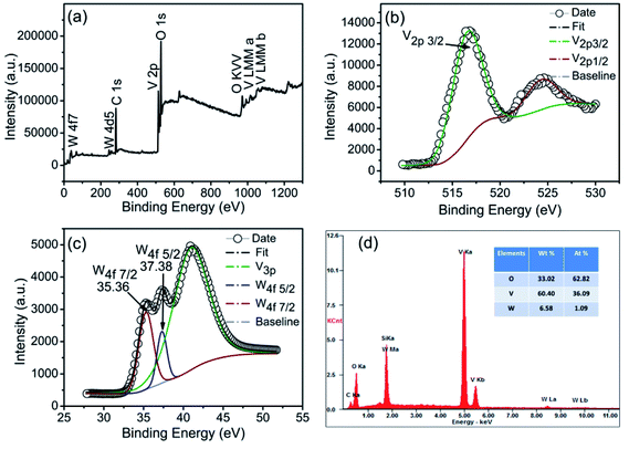 |
| | Fig. 10 (a) XPS spectra of W-doped VO2, (b and c) high-resolution spectrum of V3p and W4f, respectively, (d) EDS spectra. | |
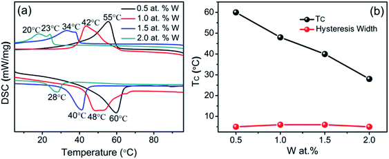 |
| | Fig. 11 (a) DSC curves of W-doped VO2, (b) phase transition temperature and hysteresis width as a function of W doping concentration. | |
4. Conclusion
In summary, VO2 (M) has been successfully synthesized through one-step hydrothermal method. H2C2O4 plays a role in adjusting the phases and dimension of VO2. This can be understood from the competition between the nucleation and growth rates. The coherent ((21)1//(2)2) and ((2)1//(020)2) interfaces between adjacent branches promote the formation of hexagonal structure. Furthermore, it is demonstrated that the VO2 (M) with hexagonal morphology improves the sensitivity and stability. The combination of hexagonal structure and W doping leads to substantially reduced phase transition temperature down to 28 °C.
Conflicts of interest
There are no conflicts to declare.
Acknowledgements
This work was jointly supported by National Natural Science Foundation of China (Grant No. 51771144, 51471130), Natural Science Foundation of Shaanxi Province (No. 2017JZ015), the fund of the State Key Laboratory of Solidification Processing in NWPU (SKLSP201708), Fundamental Research Funds for the Central Universities, City University of Hong Kong Applied Research Grant (ARG) No. 9667104.
References
- J. Liu, Q. Li, T. Wang, D. Yu and Y. Li, Angew. Chem., 2004, 116, 5158–5162 CrossRef.
- T. Y. Y. Oka, S. Sato and N. Yamamoto, J. Solid State Chem., 1998, 140, 219 CrossRef.
- L. L. B. Y. Qu, Y. Xie and B. C. Pan, Phys. Lett. A, 2011, 375, 3474 CrossRef.
- J. M. C. J. H. Park, T. S. Kasirga, C. Huang, Z. Fei, S. Hunter and D. H. Cobden, Nature, 2013, 500, 431–434 CrossRef CAS PubMed.
- S. A. Corr, M. Grossman, Y. Shi, K. R. Heier, G. D. Stucky and R. Seshadri, J. Mater. Chem., 2009, 19, 4362 RSC.
- G. Nie, L. Zhang, J. Lei, L. Yang, Z. Zhang, X. Lu and C. Wang, J. Mater. Chem. A, 2014, 2, 2910 CAS.
- Y. Gao, H. Luo, Z. Zhang, L. Kang, Z. Chen, J. Du, M. Kanehira and C. Cao, Nano Energy, 2012, 1, 221–246 CrossRef CAS.
- Q. G. J. Wu, B. S. Guiton, N. P. de Leon, L. Ouyang and H. Park, Nano Lett., 2006, 6, 2313–2317 CrossRef PubMed.
- B. Hu, Y. Ding, W. Chen, D. Kulkarni, Y. Shen, V. V. Tsukruk and Z. L. Wang, Adv. Mater., 2010, 22, 5134–5139 CrossRef CAS PubMed.
- B. Hu, Y. Zhang, W. Chen, C. Xu and Z. L. Wang, Adv. Mater., 2011, 23, 3536–3541 CrossRef CAS PubMed.
- S. Sengupta, K. Wang, K. Liu, A. K. Bhat, S. Dhara, J. Wu and M. M. Deshmukh, Appl. Phys. Lett., 2011, 99, 062114 CrossRef.
- B. Sipos, M. Duchamp, A. Magrez, L. Forró, N. Barišić, A. Kis, J. W. Seo, F. Bieri, F. Krumeich, R. Nesper and G. R. Patzke, J. Appl. Phys., 2009, 105, 074317 CrossRef.
- R. Xie, C. T. Bui, B. Varghese, Q. Zhang, C. H. Sow, B. Li and J. T. L. Thong, Adv. Funct. Mater., 2011, 21, 1602–1607 CrossRef CAS.
- N. Wang, S. Magdassi, D. Mandler and Y. Long, Thin Solid Films, 2013, 534, 594–598 CrossRef CAS.
- J. Zheng, S. Bao and P. Jin, Nano Energy, 2015, 11, 136–145 CrossRef CAS.
- C. Liu, X. Cao, A. Kamyshny, J. Y. Law, S. Magdassi and Y. Long, J. Colloid Interface Sci., 2014, 427, 49–53 CrossRef CAS PubMed.
- W. Ning, H. Yizhong, S. Magdassi, D. Mandler, L. Hai and L. Yi, RSC Adv., 2013, 3, 7124 RSC.
- K. Martens, I. P. Radu, S. Mertens, X. Shi, L. Nyns, S. Cosemans, P. Favia, H. Bender, T. Conard, M. Schaekers, S. De Gendt, V. Afanas'ev, J. A. Kittl, M. Heyns and M. Jurczak, J. Appl. Phys., 2012, 112, 124501 CrossRef.
- J. Wu, W. Huang, Q. Shi, J. Cai, D. Zhao, Y. Zhang and J. Yan, Appl. Surf. Sci., 2013, 268, 556–560 CrossRef CAS.
- S. N. P. Jin and S. Tanemura, Thin Solid Films, 1998, 324, 151 CrossRef.
- D. Vernardou, D. Louloudakis, E. Spanakis, N. Katsarakis and E. Koudoumas, Sol. Energy Mater. Sol. Cells, 2014, 128, 36–40 CrossRef CAS.
- J. Sakai, M. Zaghrioui, V. Ta Phuoc, S. Roger, C. Autret-Lambert and K. Okimura, J. Appl. Phys., 2013, 113, 123503 CrossRef.
- Y. Gao, C. Cao, L. Dai, H. Luo, M. Kanehira, Y. Ding and Z. L. Wang, Energy Environ. Sci., 2012, 5, 8708 CAS.
- J. Zhang, J. Li, P. Chen, F. Rehman, Y. Jiang, M. Cao, Y. Zhao and H. Jin, Sci. Rep., 2016, 6, 27898 CrossRef CAS PubMed.
- Y. F. G. Z. Chen, L. T. Kang, C. X. Cao, S. Chen and H. J. Luo, J. Mater. Chem. A, 2014, 2, 2718 Search PubMed.
- W. Yu, S. Li and C. Huang, RSC Adv., 2016, 6, 7113–7120 RSC.
- Y. G. C. Cao and H. Luo, J. Phys. Chem. C, 2008, 112, 18810–18814 Search PubMed.
- J. Galy, J. Solid State Chem., 1999, 148, 224–228 CrossRef CAS.
- G. N. C. Leroux and G. Van Tendeloo, Phys. Rev. B: Condens. Matter Mater. Phys., 1998, 57, 5111 CrossRef.
- M. Li, D.-B. Li, J. Pan, J.-C. Lin and G.-H. Li, Eur. J. Inorg. Chem., 2013, 2013, 1207–1212 CrossRef CAS.
- M. Li, S. Magdassi, Y. Gao and Y. Long, Small, 2017, 13, 1701147 CrossRef PubMed.
- C. Cao, Y. Gao and H. Luo, J. Phys. Chem. C, 2008, 112, 18810–18814 CAS.
- S. Ji, F. Zhang and P. Jin, J. Solid State Chem., 2011, 184, 2285–2292 CrossRef CAS.
- L. Dai, Y. Gao, C. Cao, Z. Chen, H. Luo, M. Kanehira, J. Jin and Y. Liu, RSC Adv., 2012, 2, 5265 RSC.
- M. Li, F. Kong, Y. Zhang and G. Li, CrystEngComm, 2011, 13, 2204 RSC.
- Z. Liu, M. Miyauchi, T. Yamazaki and Y. Shen, Sens. Actuators, B, 2009, 140, 514–519 CrossRef CAS.
- J. F. L. J. T. Zhang, Q. Peng, X. Wang and Y. D. Li, Chem. Mater., 2006, 18, 867–871 CrossRef CAS.
- M. J. Powell, P. Marchand, C. J. Denis, J. C. Bear, J. A. Darr and I. P. Parkin, Nanoscale, 2015, 7, 18686–18693 RSC.
- Y. Cui, S. Shi, L. Chen, H. Luo and Y. Gao, Phys. Chem. Chem. Phys., 2015, 17, 20998–21004 RSC.
- J. Zhu, Y. Zhou, B. Wang, J. Zheng, S. Ji, H. Yao, H. Luo and P. Jin, ACS Appl. Mater. Interfaces, 2015, 7, 27796–27803 CAS.
- G. X. X. Liu, C. Huang, Q. Xu, Y. Zhang and Y. Luo, Mater. Lett., 2008, 62, 1878–1880 CrossRef.
- C. J. Patridge, L. Whittaker, B. Ravel and S. Banerjee, J. Phys. Chem. C, 2012, 116, 3728–3736 CAS.
- Y. Zhang, J. Zhang, X. Zhang, S. Mo, W. Wu, F. Niu, Y. Zhong, X. Liu, C. Huang and X. Liu, J. Alloys Compd., 2013, 570, 104–113 CrossRef CAS.
Footnote |
| † Electronic supplementary information (ESI) available. See DOI: 10.1039/c8ra00716k |
|
| This journal is © The Royal Society of Chemistry 2018 |
Click here to see how this site uses Cookies. View our privacy policy here. 
 Open Access Article
 This Open Access Article is licensed under a Creative Commons Attribution-Non Commercial 3.0 Unported Licence
 ab,
Ke Wei Xuac,
Fei Ma*ab and
Paul K. Chu*b
ab,
Ke Wei Xuac,
Fei Ma*ab and
Paul K. Chu*b


