
 Open Access Article
 This Open Access Article is licensed under a Creative Commons Attribution-Non Commercial 3.0 Unported Licence
Enhancing the ambient stability of few-layer black phosphorus by surface modification
Shuang-Ying Lei*a,
Hai-Yun Shen a,
Yi-Yang Sunb,
Neng Wana,
Hong Yua and
Shengbai Zhangc
a,
Yi-Yang Sunb,
Neng Wana,
Hong Yua and
Shengbai Zhangc
aKey Laboratory of Microelectromechanical Systems of the Ministry of Education, Southeast University, Nanjing 210096, China. E-mail: lsy@seu.edu.cn
bState Key Laboratory of High Performance Ceramics and Superfine Microstructure, Shanghai Institute of Ceramics, Chinese Academy of Sciences, Shanghai 201899, China
cDepartment of Physics, Applied Physics, and Astronomy, Rensselaer Polytechnic Institute, Troy, New York 12180, USA
First published on 18th April 2018
Abstract
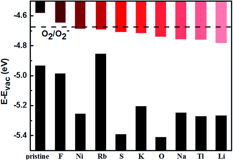
Based on high-throughput density functional theory calculations, we investigated the adsorption characteristics of various elements across the Periodic Table on few-layer black phosphorus (BP). Using the criterion that the ratio of adsorption energy (Eads) to bulk cohesive energy (Ecoh) is greater than one (Eads/Ecoh > 1), we selected fifteen elements. The adsorption of these elements on few-layer BPs could significantly shift their conduction-band minimum (CBM) downward, suggesting the possibility of preventing the few-layer BPs from oxidation if the CBM can be shifted below the O2/O2− redox potential. Our study offers an efficient approach to overcoming the technical barrier in the practical application of few-layer BPs by enhancing its ambient stability via surface modification.
Introduction
During the last decade, two-dimensional (2D) nanomaterials such as graphene and transition metal dichalcogenides (TMDCs) have attracted intensive research as promising materials for future electronics applications.1 Such 2D materials exhibit excellent electronic and optical properties that are not found in their bulk counterparts.2,3 Graphene4 and TMDCs,5–7 as alternative materials to silicon, have been studied extensively for nanoelectronics (or microelectronics) applications. Both of these materials exhibit advantages and disadvantages. Graphene has a high carrier mobility and is well suited for fabrication of field-effect transistors (FETs), but the on–off ratio is low because of its gapless nature.8 The on–off ratio of FETs made from TMDCs has increased significantly,8 whereas its carrier mobility is still low. Recently, another exciting 2D material, few-layer black phosphorus (BP), has been fabricated from bulk BP by mechanical exfoliation,9–16 suite electrochemical exfoliation,17 liquid exfoliation,18 and laser irradiation methods.19 The few-layer BP-based FETs possess a large on–off ratio of up to ∼104 to 105 and a high carrier mobility of up to 1000 cm2 V−1 s−1.9,11,20Although promising for high-performance electronic devices, few-layer BPs also have inherent drawbacks. They degrade readily in the presence of oxygen and water.21–24 The development of robust native protective methods is challenging. Many efforts have focused on the use of dielectric capping layers, such as graphene, aluminum-oxide and h-BN, to prevent few-layer BPs from contact with moisture. For example, although Al2O3 encapsulated BP-based FETs can be stable at room temperature for 17 months.25 However, such protection is too challenging to consider potential damage and contamination during the deposition.25–31
Wang et al. suggested that doping with tellurium (Te) can enhance the ambient stability and transport performance of few-layer BP devices. Te-doped few-layer BPs exhibit a high mobility of up to 1850 cm2 V−1 s−1 at room temperature and maintain a high mobility of over 200 cm2 V−1 s−1 (30% of the initial value) after several weeks under ambient conditions.33 This is in marked contrast to the undoped devices that decrease rapidly to 2% of the initial value.33 This work has inspired us to study the effect of other elements on the stability of BP in order to further improve its properties, such as mobility, and replace the rare element Te.
In this paper, we perform a high-throughput computational study by scanning the Periodic Table with an aim of finding suitable elements for stabilizing few-layer BPs in ambient environment. Our search was based on the criteria that (1) the adsorption should be thermodynamically stable against clustering of adatoms and (2) the CBM of adatom-decorated few-layer BPs should be below the O2/O2− redox potential so that oxidation can be prohibited. Several elements have been proposed to serve the purpose. The electronic structures of the decorated BPs were analyzed to understand the underlying mechanisms.
Computational methods
Our first-principles calculations were performed within the framework of density functional theory (DFT) implemented in the Vienna Ab initio Simulation Package (VASP).34 The generalized gradient approximation (GGA) with the parameterization of Perdew–Burke–Ernzerhof (PBE) was used.35 Van der Waals interactions were considered by using the vdW-DF method with the optB88 exchange functional (optB88-vdW)36,37 for geometry optimization. In all calculations, the plane-wave energy cutoff was set to 400 eV. The Brillouin zone was sampled with a 3 × 3 × 1 Monkhorst–Pack grid for 3 × 4 orthorhombic supercells (containing 48 P atoms per monolayer BP). Spin polarization was considered in our calculations. All structures were fully relaxed until the forces on each atom were less than 0.01 eV Å−1. A vacuum layer of 15 Å was introduced along the direction perpendicular to the BP layers.Results and discussion
Degradation mechanism of few-layer BP
As revealed in recent study,38 light illumination triggers few-layer BP degradation. Light absorption produces excitons in few-layer BPs. If the O2/O2− redox potential is below the CBM, O2 molecules can capture the photogenerated electrons from the conduction band and become O2− anions. The presence of O2− anions on the BP surface initiates the formation of PxOy, which readily reacts with ambient moisture to form phosphoric acid.39 This reaction results in a rapid degradation of few-layer BPs in air under light illumination. To suppress the degradation, it is critical to prevent the BPs from the initial oxidation, preferably with their CBM lower than the O2/O2− redox potential.We calculated the band structures of pristine BP from monolayer up to five-layer and determined their valence and conduction band edges with respect to the vacuum level. The O2/O2− redox potential, reported to be −4.11 eV,40,41 is also with respect to the vacuum level. So, our calculated band edge positions can be compared with the O2/O2− redox potential. According to hybrid HSE functional calculation, −4.11 eV is located between the CBM of trilayer and four-layer BPs.40 Considering that we are performing a high-throughput study and that the hybrid functional calculation is computationally highly demanding, we have used the PBE functional in this work. We followed the previous work,34,39 which corrected the value for the O2/O2− redox potential to be −4.67 eV in PBE calculations. Fig. 1 shows that the CBM of few-layer BP lowers as the thickness increases and the corrected O2/O2− redox potential is located between the CBMs of trilayer and four-layer BPs, consistent with the result from HSE calculation.40 It is worth of noting that the O2/O2− redox potential may be subject to environmental parameters, such as temperature and oxygen concentration. However, experiment suggests that the variation is relatively small.42 In this work, our focus is on the trend of the CBM versus the O2/O2− redox potential. We have therefore ignored the small environment dependence.
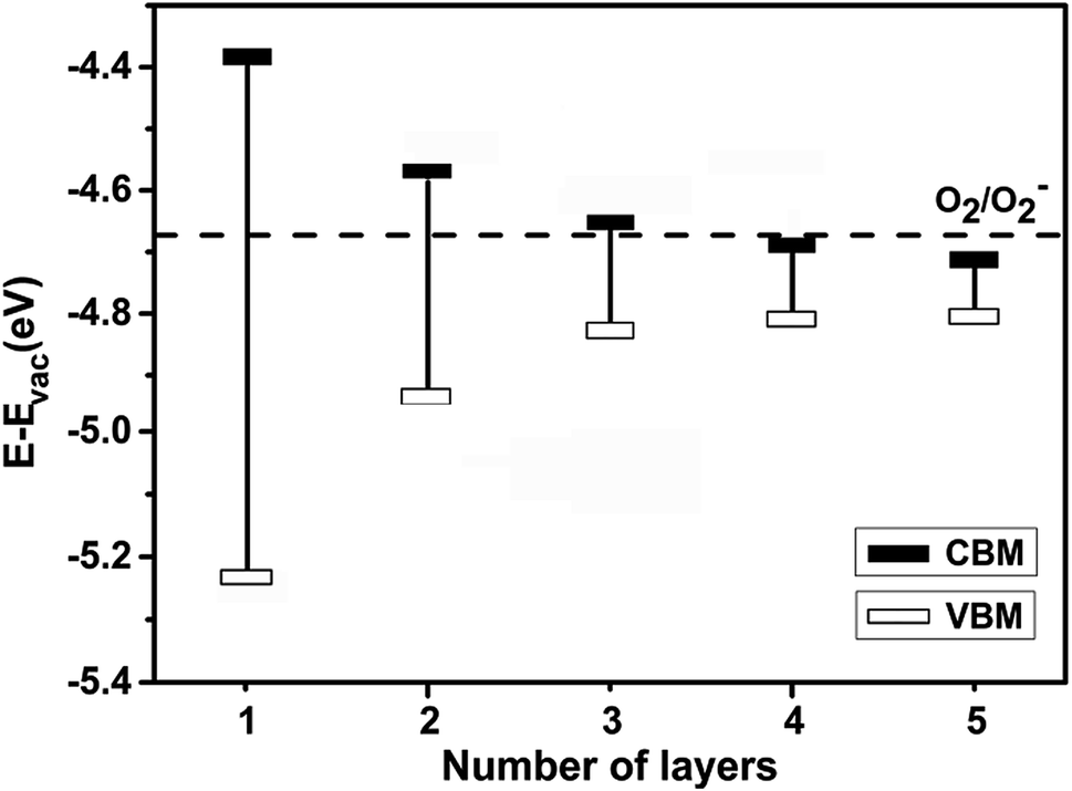 | ||
| Fig. 1 VBM and CBM of few-layer BP with respect to vacuum level. The dashed line indicates the position of the O2/O2− redox potential, as discussed in the text. | ||
Structural properties and adsorption energy
Fig. 2(a) shows the structure of monolayer BP and three possible adsorption sites, namely, hollow (H), bridge (B) and on-top (T) sites. The calculated lattice constants along the zigzag and armchair directions are 3.32 and 4.58 Å, respectively, which agree with previous study.43 Fig. 2(b) and (c) show the band structure and density of states (DOS) of pristine monolayer BP, respectively. Monolayer BP has a direct band gap of 0.85 eV from PBE calculation, which agrees well with that reported in the literature.33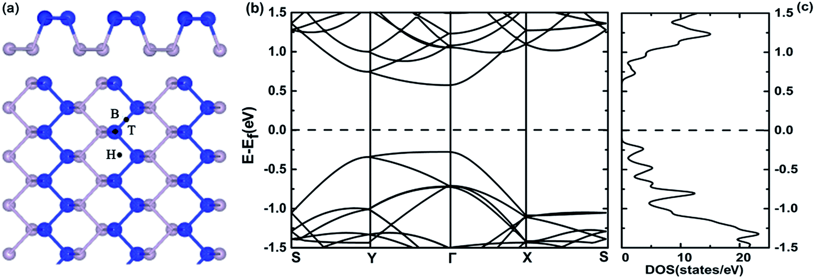 | ||
| Fig. 2 (a) Side and top views of monolayer BP and three possible adsorption sites: hollow (H), bridge (B) and top (T). The blue and grey balls represent P atoms in the top and bottom sublayers, respectively. (b) Band structure and (c) density of states (DOS) of pristine monolayer BP. | ||
To investigate the most stable adsorption position, we calculated the adsorption energy (Eads) for various adatoms on monolayer BP using:
| Eads = EA + EP − EA−P | (1) |
The adatoms could exhibit either two-dimensional (2D) or three-dimensional (3D) growth modes on a substrate. Various factors can affect the growth modes in a vapor-deposition process, such as kinetics, energetic and experimental conditions.44 Theoretically, the ratio of adsorption energy (Eads) and bulk cohesive energy (Ecoh) generally serves as a criterion to describe the growth morphology.45 Thus, we used the ratio of calculated Eads to cohesive energy (Ecoh)46 as the criterion. A ratio of Eads/Ecoh greater than 1 suggests that the adatom has stronger interaction with the substrate than that with a neighboring adatom preventing the formation of adatom clusters. In this case, the deposition usually proceeds in a 2D growth mode, which is preferred for our purpose. Otherwise, the adatoms tend to cluster and the growth proceeds in a 3D (or island) growth mode.44 Our calculated Eads/Ecoh ratios are shown in Fig. 3, which suggests that fifteen elements (Li, Na, K, Rb, Cs, Ca, Sr, Ba, Ni, Tl, La, O, S, F, and Cl) could form strong bonds with BP and prefer the 2D growth. In the following, our discussion will only focus on the decoration of few-layer BPs by the fifteen elements.
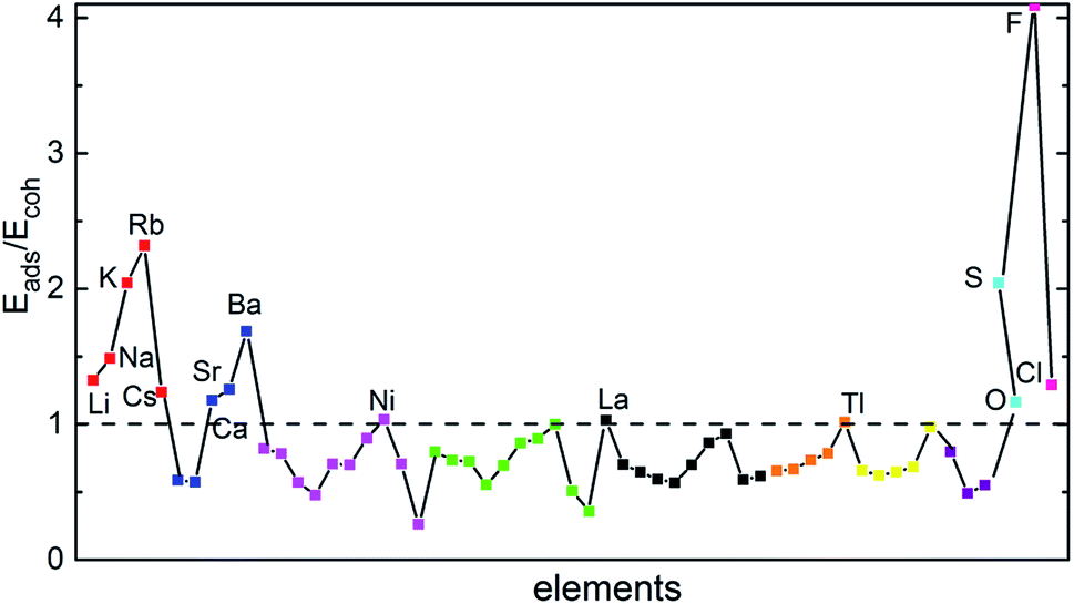 | ||
| Fig. 3 Ratio of adatom adsorption energy (Eads) to bulk cohesive energy (Ecoh). Different groups of atoms are shown in different colors: red for alkali (Li, Na, K, Rb, Cs), blue for alkaline earth (Be, Mg, Ca, Sr, Ba), magenta for 3d TM (Sc, Ti, V, Cr, Mn, Fe, Co, Ni, Cu, Zn), green for 4d TM (Y, Zr, Nb, Mo, Tc, Ru, Rh, Pd, Ag, Cd), black for 5d TM (La, Hf, Ta, W, Re, Os, Ir, Pt, Au, Hg), orange for group IIIA (B, Al, Ga, In, Tl), yellow for group IVA (C, Si, Ge, Sn, Pb), purple for group VA (N, Sb, Bi), and cyan and pink for nonmetals (O, S, F, Cl). | ||
Effect of adatoms on the CBM position of few-layer BPs
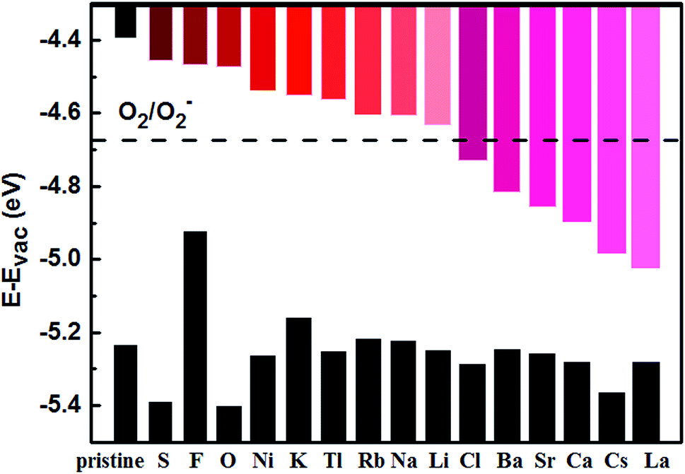 | ||
| Fig. 4 Alignment of band edges of pristine and adatom-decorated monolayer BP with the O2/O2− redox potential. | ||
Fig. 5 shows the band structures of monolayer BP decorated by Ca, Sr, Ba, Cs, La, and Cl, respectively. The group IIA adatoms (Ca, Sr and Ba) show similar effects on the band structure of pristine monolayer BP by shifting the bottom conduction band down, while leaving the top valence band nearly intact. The group IIA adatoms do not introduce spin polarization, while the electronic structure of the monolayer BP decorated by the other three adatoms, i.e., Cs, La, and Cl, is spin-polarized. For the case of Cs, the change in band structure is mainly on the spin-polarized bottom conduction bands, which are shifted down with respect to that of the pristine monolayer BP. Different from Group IIA adatoms, decoration by Cs also induces a sizable downshift of the top valence band. Among the six elements, La adatom induces the largest reduction of band gap, which is mainly resulted from the downshift of the bottom conduction band. The Cl adatom is different from the metal adatoms, which introduces two midgap levels (one spin-up and one spin-down). In this case, the band gap of the pristine monolayer BP is even increased because the downshift of top valence band is larger than the bottom conduction band. Overall, the effect induced by the six adatoms on the electronic structure of monolayer BP is sufficiently large so that the CBM has been shifted below the O2/O2− redox potential.
 | ||
| Fig. 5 Band structures of adatom-decorated monolayer BPs, where the energy zero was set to be the vacuum level. Spin-up and -down energy bands are shown in red and blue colors, respectively, for the cases of Cs, La and Cl. For comparison, the band structure of pristine monolayer BP are shown in gray color. | ||
 | ||
| Fig. 6 Band alignment of pristine and adatom-decorated bilayer BP. | ||
 | ||
| Fig. 7 Band structures of adatom-decorated bilayer BPs, where the energy zero was set to be the vacuum level. For comparison, the band structure of pristine bilayer BP are shown in gray color. | ||
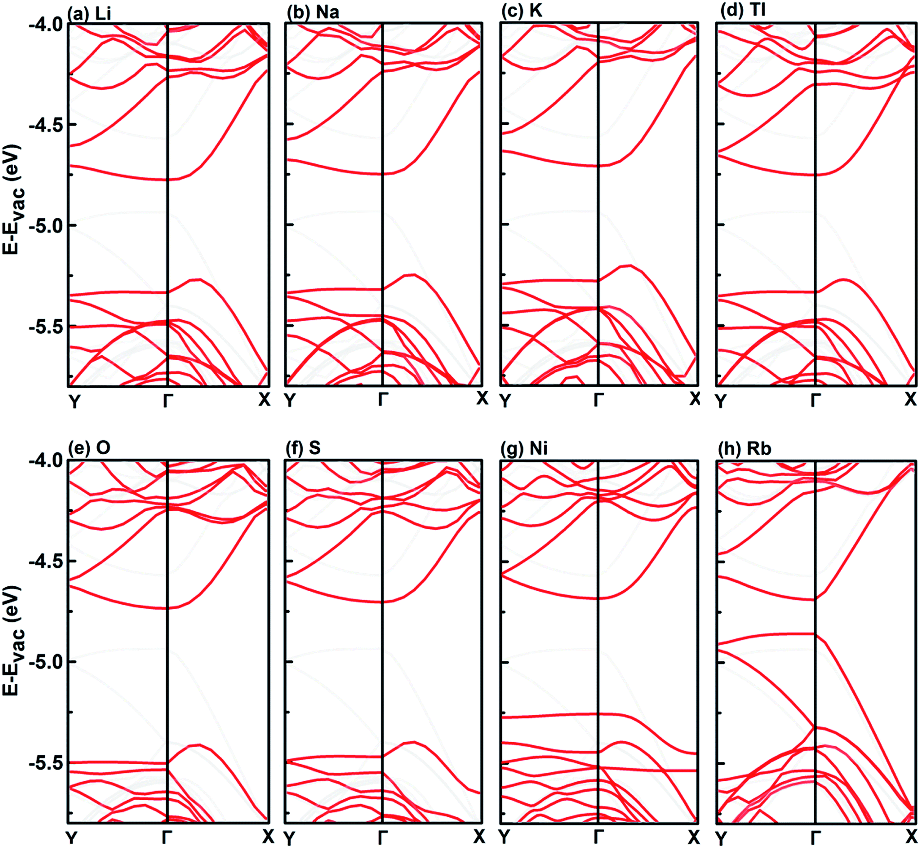
Interestingly, in the case of Li, Na, K, Tl, O, and S, an indirect gap has been induced, as a result of a bump on the top valence band along the Γ–X direction. Similar bump can also be observed in the case of Ni, but a defect band forms the top valence band covering the bump so that the band gap is still direct. In the case of Rb, the band structure is significantly different from the other group IA elements, the top valence band is shifted up, resulting in significantly reduced band gap.
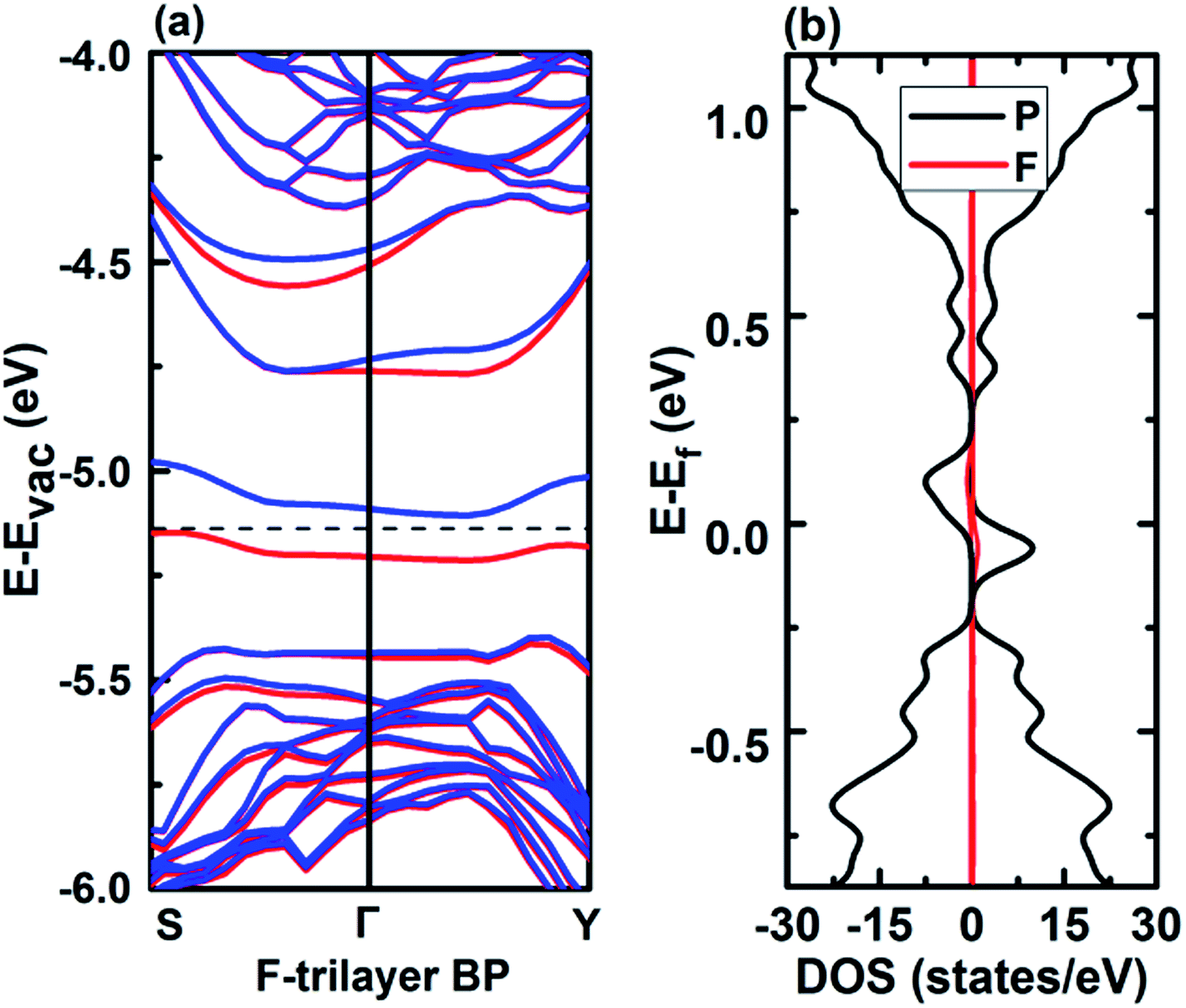 | ||
| Fig. 8 Band structure (left) and DOS (right) of F-decorated trilayer BP. Spin-up and -down bands are shown in red and blue colors, respectively. | ||
Summary
Based on first-principles DFT calculation, we studied the effect of adatom decoration on shifting the CBM of few-layer BPs, which is potentially able to enhance their stability against oxidization. A screening of most elements across the Periodic Table shows that fifteen adatoms (Li, Na, K, Rb, Cs, Ca, Sr, Ba, Ni, Tl, La, O, S, F, Cl) satisfy the criterion that the decorating atoms do not tend to form clusters. Adsorption of the selected fifteen adatoms shifts the CBM of pristine few-layer BPs significantly downward. Based on our results, all of these adatoms are expected to shift the CBM of trilayer BP to below the O2/O2− redox potential. Except for F, all the other 14 adatoms would serve the same purpose for bilayer BP. Due to the relatively large band gap of monolayer BP, only Ca, Sr, Ba, Cs, La and Cl are expected to shift its CBM below the O2/O2− redox potential. Following the previous theoretical and experimental demonstration of the effect of Te on stabilizing few-layer BPs, this study provides a useful guidance if other elements are to be explored by experiment.Author contributions
H. S. performed the calculations. S. L. and H. S. analyzed the data and wrote the manuscript. S. L., H. S., Y. S., N. W., H. Y. and S. Z. discussed and edited the manuscript.Conflicts of interest
The authors declare no competing financial interest.Acknowledgements
This work was supported by the National Science Foundation of Jiangsu Province of China (No. BK20151409), the National Basic Research Program of China (No. 2015CB352100), and the National Natural Science Foundation of China (No. 11774052, 61771137, 61370042, 11674053). The authors would like to acknowledge Shanghai Supercomputer Center.References
- V. V. Kulish, O. I. Malyi, C. Perssoncd and P. Wu, Adsorption of Metal Adatoms on Single-Layer Phosphorene, J. Phys. Chem. Phys., 2015, 17, 992–1000 RSC.
- K. S. Novoselov, A. K. Geim, S. V. Morozov, D. Jiang, M. I. Katsnelson, I. V. Grigorieva, S. V. Dubonos and A. A. Firsov, Two-Dimensional Gas of Massless Dirac Fermions in Graphene, Nature, 2005, 438, 197–200 CrossRef CAS PubMed.
- Y. Zhang, Y.-W. Tan, H. L. Stormer and P. Kim, Experimental Observation of the Quantum Hall Effect and Berry's Phase in Graphene, Nature, 2005, 438, 201–204 CrossRef CAS PubMed.
- F. Schwierz, Graphene Transistors. Nat, Nanotechnol., 2010, 5, 487–496 CAS.
- Q. H. Wang, K. Kalantar-Zadeh, A. Kis, J. N. Coleman and M. S. Strano, Electronics and Optoelectronics of Two-Dimensional Transition Metal Dichalcogenides. Nat, Nanotechnol., 2012, 7, 699–712 CAS.
- S. Z. Butler, S. M. Hollen, L. Cao, Y. Cui, J. A. Gupta, H. R. Gutierrez, T. F. Heinz, S. S. Hong and J. Huang, et al., Progress, Challenges, and Opportunities in Two-Dimensional Materials Beyond Graphene, ACS Nano, 2013, 7, 2898–2926 CrossRef CAS PubMed.
- D. Jariwala, V. K. Sangwan, L. J. Lauhon and T. J. Marks, Hersam, M. C. Emerging Device Applications for Semiconducting Two-Dimensional Transition Metal Dichalcogenides, ACS Nano, 2014, 8, 1102–1120 CrossRef CAS PubMed.
- X. Ling, H. Wang, S. Huang, F. Xia and M. S. Dresselhaus, The Renaissance of Black Phosphorus, Proc. Natl. Acad. Sci. U. S. A., 2015, 112, 4523–4530 CrossRef CAS PubMed.
- L. Li, Y. Yu, G. J. Ye, Q. Ge, X. Ou, H. Wu, D. Feng, X. H. Chen and Y. Zhang, Black Phosphorus Field-Effect Transistors. Nat, Nanotechnol., 2014, 9, 372–377 CAS.
- H. Liu, A. T. Neal, Z. Zhu, Z. Luo, X. Xu, D. Tomanek and P. D. Ye, Phosphorene: an Unexplored 2D Semiconductor with a High Hole Mobility, ACS Nano, 2014, 8, 4033–4041 CrossRef CAS PubMed.
- F. Xia, H. Wang and Y. Jia, Rediscovering Black Phosphorus: A Unique Anisotropic 2D Material for Optoelectronics and Electronics, Nat. Commun., 2014, 5, 4458 CAS.
- W. Zhu, M. N. Yogeesh, S. Yang, S. H. Aldave, J.-S. Kim, S. Sonde, L. Tao, N. Lu and D. Akinwande, Flexible Black Phosphorus Ambipolar Transistors, Circuits and AM Demodulator, Nano Lett., 2015, 15, 1883–1890 CrossRef CAS PubMed.
- H. Wang, X. Wang, F. Xia, L. Wang, H. Jiang, Q. Xia, M. L. Chin, M. Dubey and S.-J. Han, Black Phosphorus Radio-Frequency Transistors, Nano Lett., 2014, 14, 6424–6429 CrossRef CAS PubMed.
- S. Das, M. Demarteau and A. Roelofs, Ambipolar Phosphorene Field Effect Transistor, ACS Nano, 2014, 8, 11730–11738 CrossRef CAS PubMed.
- D. Xiang, C. Han, J. Wu, S. Zhong, Y. Liu, J. Lin, X.-A. Zhang, A. H. Castro Neto, A. T. S. Wee and W. Chen, Surface Transfer Doping Induced Effective Modulation on Ambipolar Characteristics of Few-Layer Black Phosphorus, Nat. Commun., 2015, 6, 6485 CrossRef CAS PubMed.
- D. J. Late, Temperature Dependent Phonon Shifts in Few-Layer Black Phosphorus, ACS Appl. Mater. Interfaces, 2015, 7, 5857–5862 CAS.
- B. E. Manisha, M. S. Pawar and D. J. Late, Humidity Sensing and Photodetection Behavior of Electrochemically Exfoliated Atomically Thin-Layered Black Phosphorus Nanosheets, ACS Appl. Mater. Interfaces, 2016, 8, 11548–11556 Search PubMed.
- D. J. Late, Liquid exfoliation of black phosphorus nanosheets and its application as humidity sensor, Microporous Mesoporous Mater., 2016, 225, 494–503 CrossRef CAS.
- S. R. Suryawanshi, M. A. More and D. J. Late, Laser exfoliation of 2D black phosphorus nanosheets and their application as a field emitter, RSC Adv., 2016, 6, 112103–112108 RSC.
- S. P. Koenig, R. A. Doganov, H. Schmidt and A. H. Castro Neto, Electric Field Effect in Ultrathin Black Phosphorus, Appl. Phys. Lett., 2014, 104, 103106 CrossRef.
- A. Ziletti, A. Carvalho, D. K. Campbell, D. F. Coker and N. A. H. Castro, Oxygen Defects in Phosphorene, Phys. Rev. Lett., 2014, 114, 046801 CrossRef PubMed.
- J. Kang, J. D. Wood, S. A. Wells, J.-H. Lee, X. Liu, K.-S. Chen and M. C. Hersam, Solvent Exfoliation of Electronic-Grade, Two-Dimensional Black Phosphorus, ACS Nano, 2015, 9, 3596–3604 CrossRef CAS PubMed.
- G. X. Wang, W. J. Slough, R. Pandey and S. P. Karna, Degradation of Phosphorene in Air: Understanding at Atomic Level, 2D Mater., 2016, 3, 025011 CrossRef.
- D. Hanlon, C. Backes, E. Doherty, C. S. Cucinotta, N. C. Berner, C. Boland, K. Lee, A. Harvey, P. Lynch and Z. Gholamvand, et al., Liquid Exfoliation of Solvent-Stabilized Few-Layer Black Phosphorus For Applications Beyond Electronics, Nat. Commun., 2015, 6, 8563 CrossRef CAS PubMed.
- Y. Y. Illarionov, M. Waltl, G. Rzepa, T. Knobloch, J. S. Kim, D. Akinwande and T. Grasser, Highly-stable black phosphorus field-effect transistors with low density of oxide traps, NPJ 2D Mater. Appl., 2017, 1, 23 CrossRef.
- J. S. Kim, Y. N. Liu, W. N. Zhu, S. Kim, D. Wu, L. Tao, A. Dodabalapur, K. Lai and D. Akinwande, Toward Air-Stable Multilayer Phosphorene Thin-Films and Transistors, Sci. Rep., 2015, 5, 8989 CrossRef CAS PubMed.
- J. D. Wood, S. A. Wells, D. Jariwala, K. S. Chen, E. Cho, V. K. Sangwan, X. L. Liu and L. J. Lauhon, et al., Effective Passivation of Exfoliated Black Phosphorus Transistors against Ambient Degradation, Nano Lett., 2014, 14, 6964 CrossRef PubMed.
- A. Avsar, I. J. Vera-Marun, J. Y. Tan, K. Watanabe, T. Taniguchi, A. H. C. Neto and B. Ozyilmaz, Air-Stable Transport in Graphene-Contacted, Fully Encapsulated Ultrathin Black Phosphorus-Based Field-Effect Transistors, ACS Nano, 2015, 9, 4138 CrossRef CAS PubMed.
- X. L. Chen, Y. Y. Wu, Z. F. Wu, Y. Han, S. G. Xu, L. Wang, W. G. Ye, T. Y. Han, Y. H. He, Y. Cai and N. Wang, High-Quality Sandwiched Black Phosphorus Heterostructure and its Quantum Oscillations, Nat. Commun., 2015, 6, 7315 CrossRef CAS PubMed.
- R. A. Doganov, E. C. QFarrell, P. Koenig, T. Yeo, A. Ziletti, A. Carvalho, D. K. Campbell, D. F. Coker, K. Watanabe and T. Taniguchi, et al., Transport Properties of Pristine Few-Layer Black Phosphorus by Van Der Waals Passivation in an Inert Atmosphere, Nat. Commun., 2015, 6, 6647 CrossRef CAS PubMed.
- Y. Zhao, H. Wang, H. Huang, Q. Xiao, Y. Xu, Z. Guo, H. Xie, J. Shao, Z. Sun and W. Han, et al., Surface Coordination of Black Phosphorus for Robust Air and Water Stability, Angew. Chem., 2016, 55, 5003–5007 CrossRef CAS PubMed.
- C. R. Ryder, J. D. Wood, S. A. Wells, Y. Yang, D. Jariwala, T. J. Marks, G. C. Schatz and M. C. Hersam, Covalent Functionalization and Passivation of Exfoliated Black Phosphorus via Aryl Diazonium Chemistry, Nat. Chem., 2016, 8, 597 CrossRef CAS PubMed.
- B. C. Yang, B. S. Wan, Q. H. Zhou, Y. Wang, W. T. Hu, W. M. Lv, Q. Chen, Z. M. Zeng, F. S. Wen and J. Y. Xiang, et al., Te-Doped Black Phosphorus Field-Effect Transistors, Adv. Mater., 2016, 28, 9408–9415 CrossRef CAS PubMed.
- G. Kresse and J. Furth, Efficiency of Ab-Initio Total Energy Calculations for Metals and Semiconductors Using a Plane-Wave Basis Set, Comput. Mater. Sci., 1996, 6, 15–50 CrossRef CAS.
- J. P. Perdew, K. Burke and M. Ernzerhof, Generalized Gradient Approximation Made Simple, Phys. Rev. Lett., 1996, 77, 3865–3868 CrossRef CAS PubMed.
- J. Klimes, D. R. Bowler and A. Michaelides, Van Der Waals Density Functionals Applied to Solids, Phys. Rev. B, 2011, 83, 195131 CrossRef.
- J. Klimes, D. R. Bowler and A. Michaelides, Chemical Accuracy for the Van Der Waals Density Functional, J. Phys.: Condens. Matter, 2010, 22, 022201 CrossRef PubMed.
- A. Favron, E. Gaufres, F. Fossard, A. L. Phaneuf-Lqheureux, N. Y. Tang, W. P. L. Levesque, A. Loiseau, R. Leonelli, S. Francoeur and R. Martel, Photooxidation and Quantum Confinement Effects in Exfoliated Black Phosphorus, Nat. Mater., 2015, 14, 826 CrossRef CAS PubMed.
- Q. H. Zhou, Q. Chen, Y. L. Tong and J. L. Wang, Light-Induced Ambient Degradation of Few-Layer Black Phosphorus: Mechanism and Protection, Angew. Chem., 2016, 55, 11437–11441 CrossRef CAS PubMed.
- L. L. Pierre, S. S. Sabri, C. M. Aguirre, J. Guillemette, M. Siaj, P. Desjardins, T. Szkopek and R. Martel, Probing Charge Transfer at Surfaces Using Graphene Transistors, Nano Lett., 2011, 11(1), 132 CrossRef PubMed.
- K. M. Ervin, I. Anusiewicz, P. Skurski, J. Simons and W. C. Lineberger, The Only Stable State of O2-Is the X2Πg Ground State and It (Still!) Has an Adiabatic Electron Detachment Energy of 0.45 eV, J. Phys. Chem. A, 2003, 107, 8521–8529 CrossRef CAS.
- A. Favron, E. Gaufres, F. Fossard, A. L. Phaneuf-LQHeureux, N. Y. W. Tang, P. L. Levesque, A. Loiseau, R. Leonelli, S. Francoeur and R. Martel, Exfoliating black phosphorus down to the monolayer: photo-induced oxidation and electronic confinement effects, Nat. Mater., 2015, 14, 826 CrossRef CAS PubMed.
- H. Liu, A. T. Neal, Z. Zhu, Z. Luo, X. Xu, D. Tománek and P. D. Ye, Phosphorene: an Unexplored 2D Semiconductor With a High Hole Mobility, ACS Nano, 2014, 8, 4033 CrossRef CAS PubMed.
- T. Hu and J. S. Hong, First-Principles Study of Metal Adatom Adsorption on Black Phosphorene, J. Phys. Chem. C, 2015, 119, 8199–8207 CAS.
- X. Liu, C. Z. Wang, M. Hupalo, W. C. Lu, M. C. Tringides, Y. X. Yao and K. M. Ho, Metals on Graphene: Correlation between Adatom Adsorption Behavior and Growth Morphology, Phys. Chem. Chem. Phys., 2012, 14(25), 9157 RSC.
- C. Kittel, Introduction to Solid State Physics, Wiley, Hoboken, NJ, 8th edn, 2005 Search PubMed.
| This journal is © The Royal Society of Chemistry 2018 |