
 Open Access Article
 This Open Access Article is licensed under a Creative Commons Attribution-Non Commercial 3.0 Unported Licence
Self-powered SBD solar-blind photodetector fabricated on the single crystal of β-Ga2O3
Chao Yangab,
Hongwei Liang *b,
Zhenzhong Zhangc,
Xiaochuan Xiab,
Pengcheng Taoa,
Yuanpeng Chenab,
HeQiu Zhangb,
Rensheng Shenb,
Yingmin Luob and
Guotong Dub
*b,
Zhenzhong Zhangc,
Xiaochuan Xiab,
Pengcheng Taoa,
Yuanpeng Chenab,
HeQiu Zhangb,
Rensheng Shenb,
Yingmin Luob and
Guotong Dub
aSchool of Physics, Dalian University of Technology, Dalian 116024, China. E-mail: hwliang@dlut.edu.cn
bSchool of Microelectronics, Dalian University of Technology, Dalian 116024, China
cState Key Laboratory of Luminescence and Applications, Changchun Institute of Optics, Fine Mechanics and Physics, Chinese Academy of Sciences, Changchun 130033, China
First published on 8th February 2018
Abstract
A Schottky barrier diode (SBD) solar-blind photodetector was fabricated based on the single crystal β-Ga2O3. Cu and Ti/Au were deposited on the top and bottom surface of Ga2O3 as Schottky and ohmic contacts, respectively. The SBD exhibits a higher rectification ratio of up to 5 × 10⁷ at ±2 V. The photoresponse spectra show a maximum responsivity at 241 nm and a cutoff wavelength of 256 nm. The solar-blind/ultraviolet and solar-blind/visible rejection ratio can reach a high level of up to 200 and 1000, respectively. It is interesting that the device has a clear response to the solar-blind wavelength at zero bias, which confirms it can be used as a self-powered solar-blind photodetector.
Introduction
The solar radiation in the range of 200–280 nm cannot reach the earth's surface due to the absorption by ozone so that the ultraviolet (UV) light in this range is appropriate for communication as a ‘black background’.1,2 If a photodetector working in this range has no response to solar radiation, the photodetector is called a solar-blind photodetector. Nowadays the solar-blind photodetector has been widely applied in many fields such as missile warning, fire alarms, ozone monitoring, under water and space communication, and so on.3–5Currently, the materials suitable for fabricating solar-blind photodetectors include AlGaN, MgZnO and Ga2O3. Both AlGaN and MgZnO are ternary alloys, which require complex processes to obtain high Al1 and Mg6 content materials. β-Ga2O3 is one of the best materials for solar-blind photodetector fabrication due to its wide bandgap of 4.9 eV (≈253 nm), which locates at the center position of the solar-blind wavelength. More importantly, large size and high quality Ga2O3 single crystals can be prepared through conventional methods such as floating zone (FZ),7 edge-defined film-fed growth (EFG)8 and Czochralski (CZ)9 methods. Ga2O3 solar-blind photodetectors are now mainly fabricated on thin films with a variety of film growth technique such as PLD,10 MBE,11 MOCVD12 and radio-frequency magnetron sputtering,13 and on nanostructures i.e. nanowires,14 rods,15 belts16 and arrays.17 However, defects introduced during these growth methods can trap and de-trap the photogenerated carriers within the deep levels, which could cause photocurrent persistence for an extended period (from approximately a few minutes to hours) after the excitation light is shut off, and this phenomenon is called the persistent photoconductivity (PPC) effect.16,18 Single crystal material can reduce the defects density to a very low level and increase the device response speed. And eliminating the influences of defects19 and narrow band gap heterojunction substrate,20 the response range of the single crystal Ga2O3 photodetector can be limited sharply to solar-blind wavelength. Moreover, the photodetector based on a single crystal can be operated with a low dark current density, which can increase the device sensitivity. Besides, when prospecting the application of avalanche photodetector, single crystal material would be a better choice for the high resistance to avalanche current due to the perfect crystalline quality.
Traditional photodetectors typically require an external bias as the driving force to prevent the recombination of photogenerated carriers.21 However, the external power sources limit their independence in application as the size of the power sources always far exceed that of detectors. Nowadays, it is highly desirable for the photodetector to function independently of external power sources. It has been common in the previous reports to call devices of this type “self-powered”.18,22,23 Self-powered detectors decrease energy consumption and are more environmentally friendly. Combined with wireless technology, self-powered detectors present greater adaptability and sustainability, even used in unattended hazardous atmosphere or harsh environment. Self-power can be achieved by photovoltaic effect by means of p–n junction, heterojunction and Schottky junction. When UV lights incidents into the devices, built-in electric field in these structures can separate photogenerated electron–hole pairs and output the electrical signal.24,25
In this work, the self-powered Ga2O3 Schottky barrier diode (SBD) solar-blind photodetector was fabricated with the deposition of Cu and Ti/Au on the top and bottom surfaces of Ga2O3 single crystal substrate, acting as Schottky and ohmic contact respectively. And the current–voltage (I–V) and photoresponse characteristics of the photodetector were investigated.
Experimental
The commercial (![[2 with combining macron]](https://www.rsc.org/images/entities/char_0032_0304.gif) 01)-orient β-Ga2O3 substrate with 680 μm thickness was used to fabricate the SBD by cutting along the [010] and [102] orientation into a 5 × 5 mm2 piece. The unintentional doped Ga2O3 crystal is n-type with a carrier concentration of about 1017 cm−3. The samples were firstly cleaned using methanol (5 min)/acetone (5 min)/methanol (5 min)/deionized water (5 min) successively. Next, the samples were etched in the solution with H2SO4
01)-orient β-Ga2O3 substrate with 680 μm thickness was used to fabricate the SBD by cutting along the [010] and [102] orientation into a 5 × 5 mm2 piece. The unintentional doped Ga2O3 crystal is n-type with a carrier concentration of about 1017 cm−3. The samples were firstly cleaned using methanol (5 min)/acetone (5 min)/methanol (5 min)/deionized water (5 min) successively. Next, the samples were etched in the solution with H2SO4![[thin space (1/6-em)]](https://www.rsc.org/images/entities/char_2009.gif) :H2O2:H2O = 4:1:1 for 5 min. Finally, the samples were dipped in 90 °C deionized water until the temperature cooling down to room temperature. The metal deposition was performed by vacuum thermal evaporation method. Ohmic contact electrode was fabricated firstly with Ti/Au (20 nm/200 nm) deposition on the bottom surface of the Ga2O3 substrate followed by 500 °C annealing in nitrogen for 3 min. Then Cu (20 nm) was deposited on the top surface of the Ga2O3 substrate with 150 °C annealing in nitrogen for 5 min as the Schottky contact electrode. The schematic structure of the detector is shown in the inset of Fig. 1.
:H2O2:H2O = 4:1:1 for 5 min. Finally, the samples were dipped in 90 °C deionized water until the temperature cooling down to room temperature. The metal deposition was performed by vacuum thermal evaporation method. Ohmic contact electrode was fabricated firstly with Ti/Au (20 nm/200 nm) deposition on the bottom surface of the Ga2O3 substrate followed by 500 °C annealing in nitrogen for 3 min. Then Cu (20 nm) was deposited on the top surface of the Ga2O3 substrate with 150 °C annealing in nitrogen for 5 min as the Schottky contact electrode. The schematic structure of the detector is shown in the inset of Fig. 1.
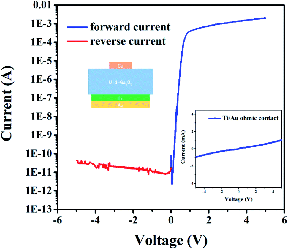 | ||
| Fig. 1 I–V characteristics of the Ga2O3 solar-blind photodetector at dark condition. The inset depicts the ohmic contact characterize on the bottom side of the single crystal Ga2O3. | ||
X-ray diffraction (XRD) measurement was carried out to determine crystalline quality using Bruker D8 DISCOVER diffractometer. The I–V characteristics for the SBD were measured using Keithley 4200-SCS semiconductor characterization system. Time-resolved photocurrent response spectrum was conducted under 254 nm light with Keithley 4200-SCS semiconductor characterization system. The photoresponse spectra of the photodetectors were measured in a SPEX scanning monochromator employing a 150 W Xe lamp as the illumination source. The spectrum of the Xe lamp can cover from 200 nm to over 1000 nm, and the responsivity spectrum was obtained by measuring the photocurrent (calibrated with a standard Si photodiode) under the illumination of the Xe lamp spectrum from 200 nm to 500 nm using the scanning monochromator.
Results and discussion
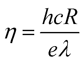
XRD rocking curve measurement was carried out to determine the crystalline quality of the single crystal Ga2O3. The full width at half maximum (FWHM) values of (![[6 with combining macron]](https://www.rsc.org/images/entities/char_0036_0304.gif) 03) diffraction peak is 42.2 arcsec (figure not shown here), which confirms good crystalline quality. The I–V characteristics of the photodetector were obtained at dark condition, as shown in Fig. 1. Linear characteristic for the bottom electrode is shown in the inset, which indicates ohmic contacts between Ga2O3 and Ti/Au electrode. In Fig. 1, the forward current is linear in the semilogarithmic scale at low forward bias voltages and deviates from linearity due to the effect of series resistance Rs. The reverse current increases slightly, which is probably caused by barrier height inhomogeneities.26 The forward current can reach above milliamp order of magnitude and the reverse current is about sub-nanoamp order of magnitude. The SBD exhibits a higher rectification ratio at ±2 V up to 5 × 10⁷. Assuming that thermionic emission is the dominant current transport mechanism in the SBD, and taking into account the effect of series resistance Rs, the diode equations can be written as eqn (1):27–29
03) diffraction peak is 42.2 arcsec (figure not shown here), which confirms good crystalline quality. The I–V characteristics of the photodetector were obtained at dark condition, as shown in Fig. 1. Linear characteristic for the bottom electrode is shown in the inset, which indicates ohmic contacts between Ga2O3 and Ti/Au electrode. In Fig. 1, the forward current is linear in the semilogarithmic scale at low forward bias voltages and deviates from linearity due to the effect of series resistance Rs. The reverse current increases slightly, which is probably caused by barrier height inhomogeneities.26 The forward current can reach above milliamp order of magnitude and the reverse current is about sub-nanoamp order of magnitude. The SBD exhibits a higher rectification ratio at ±2 V up to 5 × 10⁷. Assuming that thermionic emission is the dominant current transport mechanism in the SBD, and taking into account the effect of series resistance Rs, the diode equations can be written as eqn (1):27–29
 | (1) |
The response speed is an important parameter for photodetector, which can be used to evaluate the detection performance to the fast-varying signal. Time-resolved photocurrent response spectrum was measured with on/off switching of 254 nm light under a working bias of −20 V, as shown in Fig. 2. The 10–90% rise time is estimated to be 0.729 s and 90–10% decay time to be 1.209 s and no long time PPC effect is observed due to the high crystalline quality. This PPC phenomenon is generally found in the Ga2O3 thin film and nanostructure photodetectors.32,33 The on and off state current for six cycles remain the same level, which indicates the high reversibility and high reproducibility of the Ga2O3 solar-blind photodetector.
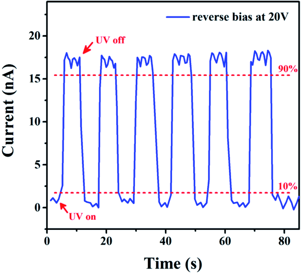 | ||
| Fig. 2 Time-resolved photocurrent spectrum with the UV light (253 nm) of photodetector at −20 voltage. | ||
Fig. 3(a) is the photoresponse spectra under different reverse voltages up to 35 V. The responsivity at peaks increases obviously at low bias range, while it increases slowly at high bias range due to the recombination as the photogenerated carriers transport through the single crystal. The responsivity of the photodetector can be calculated by eqn (2):34
 | (2) |
 | (3) |
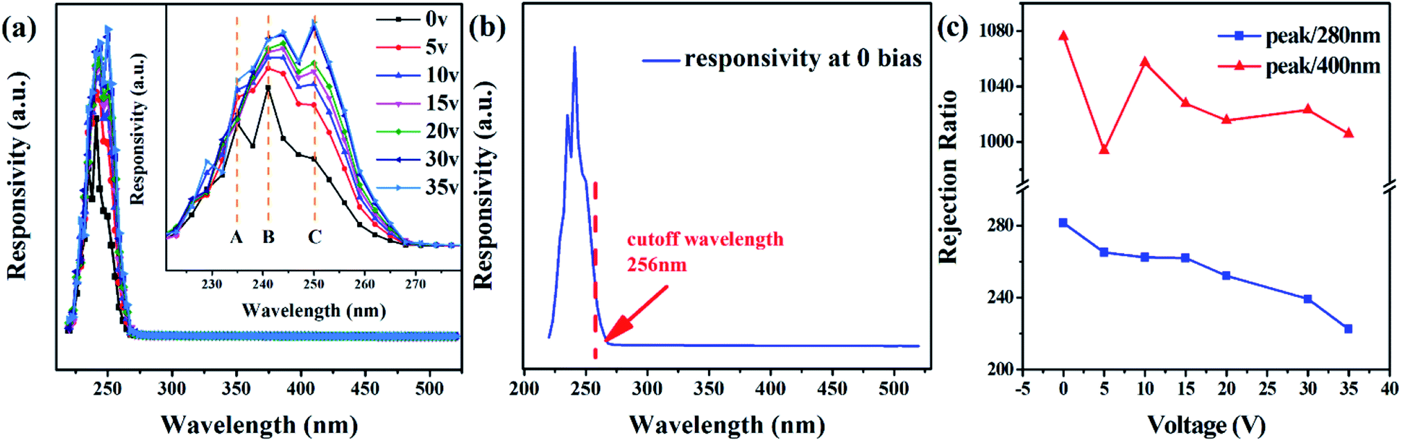 | ||
| Fig. 3 Photoresponse characteristics for the photodetector: (a) responsivity at different bias, (b) responsivity at 0 bias, (c) solar-blind/visible and solar-blind/UV rejection ratio at different bias. | ||
The responsivity at solar-blind wavelength range exhibit three peaks, as shown in the inset of Fig. 3(a). All of them changes in different trends as the reverse bias increases, as shown in Fig. 4. This phenomenon can be explained by the different absorption mechanisms of Ga2O3 to different wavelengths of UV light. According to Medvedeva's calculation,35 states of s, p and d of the cations in Ga2O3 all contributes to the conduction band. Due to the different degree of the orbitals hybridization, the electrons have different velocities on various orbitals. We assume that UV light with different wavelengths excited electrons to different orbitals, which caused different variation trends as the increasing bias. A further investigation will be required to obtain a better understanding of the absorption mechanisms.
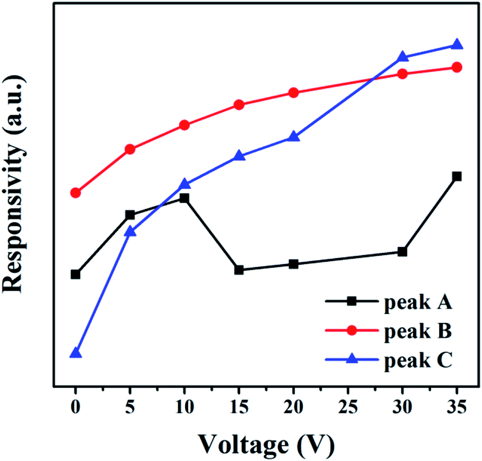 | ||
| Fig. 4 Intensity of three peaks in the photoresponse spectra at different bias. | ||
Conclusions
Cu SBD solar-blind photodetector has been successfully fabricated based on the single crystal β-Ga2O3. The SBD exhibited a higher rectification ratio up to 5 × 10⁷ at ±2 V. The photoresponse spectrum shows a maximum responsivity at 241 nm and a cutoff wavelength of 256 nm. The low dark current and sharp cutoff wavelength result from the high crystalline quality. The device has a clear response to solar-blind wavelength at zero bias, which confirms it can be used as a self-powered solar-blind photodetector.Conflicts of interest
There are no conflicts to declare.Acknowledgements
This work was supported by National Natural Science Foundation of China (No. 61574026, 11675198), National Key R&D Plan (No. 2016YFB0400600, 2016YFB0400601), the Fundamental Research Funds for the Central Universities (No. DUT15LK15, DUT15RC(3)016, DUT16LK29), Liaoning Provincial Natural Science Foundation of China (No. 201602453, 201602176), China Postdoctoral Science Foundation Funded Project (No. 2016M591434).References
- L. Sang, M. Liao and M. Sumiya, Sensors, 2013, 13, 10482–10518 CrossRef CAS PubMed.
- M. Razeghi and A. Rogalski, J. Appl. Phys., 1996, 79, 7433–7473 CrossRef CAS.
- M. Razeghi, Proc. IEEE, 2002, 90, 1006–1014 CrossRef CAS.
- E. Monroy, F. Omnès and F. Calle, Semicond. Sci. Technol., 2003, 18, R33 CrossRef CAS.
- Z. Xu and B. M. Sadler, IEEE Commun. Mag., 2008, 46, 67–73 Search PubMed.
- M.-M. Fan, K.-W. Liu, X. Chen, X. Wang, Z.-Z. Zhang, B.-H. Li and D.-Z. Shen, ACS Appl. Mater. Interfaces, 2015, 7, 20600–20606 CAS.
- N. Ueda, H. Hosono, R. Waseda and H. Kawazoe, Appl. Phys. Lett., 1997, 70, 3561–3563 CrossRef CAS.
- H. Aida, K. Nishiguchi, H. Takeda, N. Aota, K. Sunakawa and Y. Yaguchi, Jpn. J. Appl. Phys., 2008, 47, 8506–8509 CrossRef CAS.
- Y. Tomm, P. Reiche, D. Klimm and T. Fukuda, J. Cryst. Growth, 2000, 220, 510–514 CrossRef CAS.
- X. C. Guo, N. H. Hao, D. Y. Guo, Z. P. Wu, Y. H. An, X. L. Chu, L. H. Li, P. G. Li, M. Lei and W. H. Tang, J. Alloys Compd., 2016, 660, 136–140 CrossRef CAS.
- X. Chen, Y. Xu, D. Zhou, S. Yang, F.-F. Ren, H. Lu, K. Tang, S. Gu, R. Zhang, Y. Zheng and J. Ye, ACS Appl. Mater. Interfaces, 2017, 9, 36997–37005 CAS.
- G. C. Hu, C. X. Shan, N. Zhang, M. M. Jiang, S. P. Wang and D. Z. Shen, Opt. Express, 2015, 23, 13554–13561 CrossRef CAS PubMed.
- D. Guo, H. Liu, P. Li, Z. Wu, S. Wang, C. Cui, C. Li and W. Tang, ACS Appl. Mater. Interfaces, 2017, 9, 1619–1628 CAS.
- Y. Li, T. Tokizono, M. Liao, M. Zhong, Y. Koide, I. Yamada and J.-J. Delaunay, Adv. Funct. Mater., 2010, 20, 3972–3978 CrossRef CAS.
- B. Zhao, F. Wang, H. Chen, Y. Wang, M. Jiang, X. Fang and D. Zhao, Nano Lett., 2015, 15, 3988–3993 CrossRef CAS PubMed.
- S. Oh, M. A. Mastro, M. J. Tadjer and J. Kim, ECS J. Solid State Sci. Technol., 2017, 6, Q79–Q83 CrossRef CAS.
- X. Chen, K. W. Liu, Z. Z. Zhang, C. R. Wang, B. H. Li, H. F. Zhao, D. X. Zhao and D. Z. Shen, ACS Appl. Mater. Interfaces, 2016, 8, 4185–4191 CAS.
- B. Zhao, F. Wang, H. Chen, L. Zheng, L. Su, D. Zhao and X. Fang, Adv. Funct. Mater., 2017, 27, 1700264 CrossRef.
- F. Alema, B. Hertog, O. Ledyaev, D. Volovik, G. Thoma, R. Miller, A. Osinsky, P. Mukhopadhyay, S. Bakhshi, H. Ali and W. V. Schoenfeld, Phys. Status Solidi A, 2017, 214, 1600688 CrossRef.
- W. Y. Weng, T. J. Hsueh, S. J. Chang, G. J. Huang and H. T. Hsueh, IEEE Photonics Technol. Lett., 2011, 23, 444–446 CrossRef CAS.
- S. M. Hatch, J. Briscoe and S. Dunn, Adv. Mater., 2013, 25, 867–871 CrossRef CAS PubMed.
- Y. Q. Bie, Z. M. Liao, H. Z. Zhang, G. R. Li, Y. Ye, Y. B. Zhou, J. Xu, Z. X. Qin, L. Dai and D. P. Yu, Adv. Mater., 2011, 23, 649–653 CrossRef CAS PubMed.
- J. J. Hassan, M. A. Mahdi, S. J. Kasim, N. M. Ahmed, H. Abu Hassan and Z. Hassan, Appl. Phys. Lett., 2012, 101, 261108 CrossRef.
- H. Chen, K. Liu, L. Hu, A. A. Al-Ghamdi and X. Fang, Mater. Today, 2015, 18, 493–502 CrossRef CAS.
- H. Chen, P. Yu, Z. Zhang, F. Teng, L. Zheng, K. Hu and X. Fang, Small, 2016, 12, 5809–5816 CrossRef CAS PubMed.
- D. Splith, S. Muller, F. Schmidt, H. von Wenckstern, J. J. van Rensburg, W. E. Meyer and M. Grundmann, Phys. Status Solidi A, 2014, 211, 40–47 CrossRef CAS.
- D. K. Schroder, Semiconductor material and device characterization, John Wiley & Sons, Hoboken, 3rd edn, 2006 Search PubMed.
- E. H. Rhoderick and R. H. Williams, Metal-semiconductor contacts, Clarendon, Oxford, 2nd edn, 1988 Search PubMed.
- S. M. Sze and K. K. Ng, Physics of semiconductor devices, John Wiley & sons, Hoboken, 3rd edn, 2006 Search PubMed.
- K. Sasaki, M. Higashiwaki, A. Kuramata, T. Masui and S. Yamakoshi, IEEE Electron Device Lett., 2013, 34, 493–495 CrossRef CAS.
- H. He, R. Orlando, M. A. Blanco, R. Pandey, E. Amzallag, I. Baraille and M. Rérat, Phys. Rev. B: Condens. Matter Mater. Phys., 2006, 74, 195123 CrossRef.
- D. Y. Guo, Z. P. Wu, Y. H. An, X. C. Guo, X. L. Chu, C. L. Sun, L. H. Li, P. G. Li and W. H. Tang, Appl. Phys. Lett., 2014, 105, 023507 CrossRef.
- Y. H. An, D. Y. Guo, Z. M. Li, Z. P. Wu, Y. S. Zhi, W. Cui, X. L. Zhao, P. G. Li and W. H. Tang, RSC Adv., 2016, 6, 66924–66929 RSC.
- W.-Y. Kong, G.-A. Wu, K.-Y. Wang, T.-F. Zhang, Y.-F. Zou, D.-D. Wang and L.-B. Luo, Adv. Mater., 2016, 28, 10725 CrossRef CAS PubMed.
- J. E. Medvedeva and C. L. Hettiarachchi, Phys. Rev. B: Condens. Matter Mater. Phys., 2010, 81, 125116 CrossRef.
| This journal is © The Royal Society of Chemistry 2018 |