
 Open Access Article
 This Open Access Article is licensed under a
 Creative Commons Attribution 3.0 Unported Licence
High-efficiency and stable piezo-phototronic organic perovskite solar cell
Ke Gu†
a,
Dongqi Zheng†a,
Lijie Li *b and
Yan Zhang*acd
*b and
Yan Zhang*acd
aSchool of Electronic Science and Engineering, School of Physics, School of Physical Electronics, University of Electronic Science and Technology of China, Chengdu 610054, China
bMultidisciplinary Nanotechnology Centre, College of Engineering, Swansea University, Swansea, SA1 8EN, UK. E-mail: L.Li@swansea.ac.uk
cBeijing Institute of Nanoenergy and Nanosystems, Chinese Academy of Sciences, Beijing 100083, China. E-mail: zhangyan@uestc.edu.cn
dCollege of Nanoscience and Technology, University of Chinese Academy of Sciences, Beijing 100049, China
First published on 27th February 2018
Abstract
Perovskite materials are regarded as next-generation organic photovoltaic (OPV) materials due to their excellent physical and chemical properties. Recent theoretical and experimental advances also revealed the piezoelectric properties of CH3NH3PbI3 perovskite thin films. In this work, a CH3NH3PbI3 perovskite piezo-phototronic solar cell is studied in theory. The output parameters such as open circuit voltage, current–voltage characteristics, fill factor, power conversion efficiency, and maximum output power with external strains are presented. The coefficient to characterize piezo-phototronic modulation is also calculated for the piezo-phototronic solar cell. With the change of strain, the output performance can be controlled and enhanced. This principle can offer not only a novel and unique approach to produce high-performance, stable perovskite solar cells, but also a principle to design new piezoelectric perovskite optoelectronic devices.
1. Introduction
Organic photovoltaic (OPV) devices have been leading the research into energy science and technology.1–3 In recent years, much attention has been devoted to the perovskite materials and their applications in solar energy conversion because of their high absorbance, low carrier recombination rate, outstanding ferroelectric properties and easier synthesis.4–6 Among them, perovskite solar cells (PSC) with CH3NH3PbX3 perovskites (X = Cl, Pb, and I) as absorber layers show great potential in fabricating low-cost and large-scale commercial solar cells, whose efficiency has increased from 3.8% to over 22% in the past five years.7–10The concept of piezoelectric enhanced performance of nanostructure semiconductor device were put forward in 2007, promoting the interdisciplinary development in the field of nanotechnology.11 Combining piezoelectric and semiconductor properties, piezoelectric semiconductor materials such as ZnO, GaN, CdS have been used to fabricate multifunctional stretchable semiconductor devices, such as flexible photodetectors,12 piezophototronic light emitting diodes13 and piezo-nanogenerator.14 Besides, piezo-phototronic and pyro-phototronic effect also enables the improvement in power conversion efficiency of low-dimensional solar cells.15–18
Recent breakthrough in photovoltaic devices has developed a stable and durable CH3NH3PbI3 perovskite solar cell with a stable efficiency of 8%, which overcomes the problem of PSC's application in the ambient environment.19 CH3NH3PbI3 thin films have the piezoelectric properties in recent experiments.20 Piezoelectric materials have been used to design energy harvesting devices, such as piezoelectric generator.21
From semiconductor physics point of view, light management and carrier management are two critical factors determining the performance of solar cells.22 The basic principle of a solar cell is that photo-generated electron–hole pairs are separated on the interface of metal–semiconductor or p–n junction. In piezo-phototronic solar cell, piezoelectric charges increase the built-in electric field, which can efficiently enhance the separation of electron–hole pairs and improve the carrier management.15 The piezo-phototronic perovskite solar cells can be a promising candidate for flexible OPV devices. There are several newly discovered semiconductor properties of CH3NH3Pb3I3. The large piezoelectric constant (0.83 C m−2) and the small relative dielectric constant (32) of the perovskite materials result in higher current density and higher adjustability. The adjustability shows the higher modulation of output parameters including open-circuit voltage, output power density, fill factor, PCE as well as the regulator further presented. Besides, the stable and durable CH3NH3PbI3 also demonstrates perfect output characteristics with short circuit current density as 14 mA cm−2 and open circuit voltage as 0.45 V, comparable to other novel solar energy conversions, which sets the foundation for the high-performance PPSC.19
This work provides a prototype of the perovskite piezo-phototronic solar cell, which has improved performances by applying piezoelectric and photovoltaic properties of CH3NH3PbI3 thin films. A schematic of the device architecture is shown in Fig. 1. The main structure is the perovskite material sandwiched by CuI (as HTM) and TiO2 (as ETM). The upper layer is an Au electrode, while the base is the PET substrate. Here, we treat the interface between the top layer and the layer beneath as metal–semiconductor (M–S) contact, and the bottom contact (between the base layer and the layer on its top) as ohmic contact. When compressive and tensile strains are applied on the CH3NH3PbI3 layer, the piezoelectric polarization charges are induced at the contact. Fig. 1(b) and (c) show the modulation role in the Schottky barrier played by piezoelectric field, which can increase or decrease the barrier respectively. The characteristic parameters to measure the performance of solar cells, such as current–voltage characteristics, open circuit voltage, maximum output power, fill factor, and power conversion efficiency are studied. The principle of piezo-phototronic solar cell can offer a unique and novel approach to produce an organic photovoltaic cell with stability, higher efficiency and lower cost.
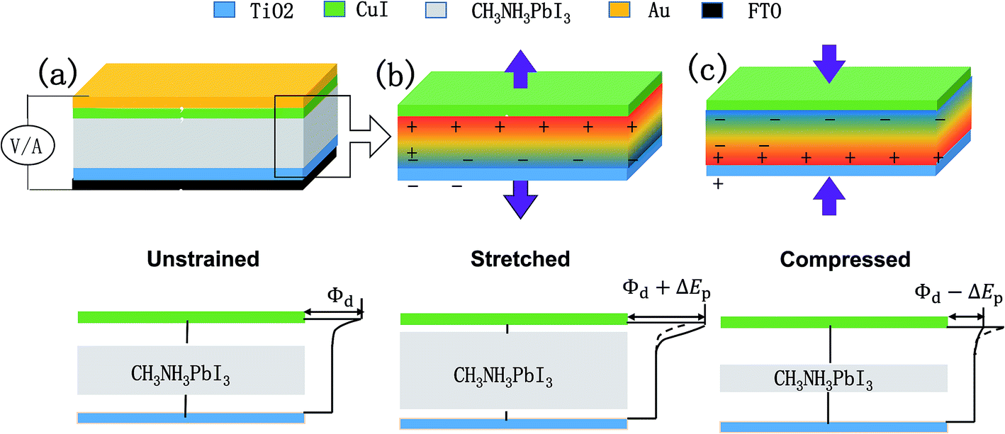 | ||
| Fig. 1 (a) Schematic and energy band diagram of a piezo-phototronic perovskite solar cell. (b) Schematics and energy band diagram of the PPSC with tensile strain applied. (c) Schematics and energy band diagram of the PPSC with compressive strain applied. The transitional color indicates the distribution of the piezo-potential on the CH3NH3PbI3 thin film. | ||
2. Piezo-phototronic modulation on PPSC
Previous research works have elucidated the characteristics of piezo-phototronic solar cell by semiconductor physics and piezoelectric theory. Here, the detailed PPSC theoretical analysis is presented combining the physics-based analytical model for perovskite solar cells23 and piezo-phototronic theory. Given the extraordinarily long diffusion length,24,25 the recombination in the perovskite layer is ignored, so the analytical model of diffusion and drift of photo-generated carriers can be derived as:
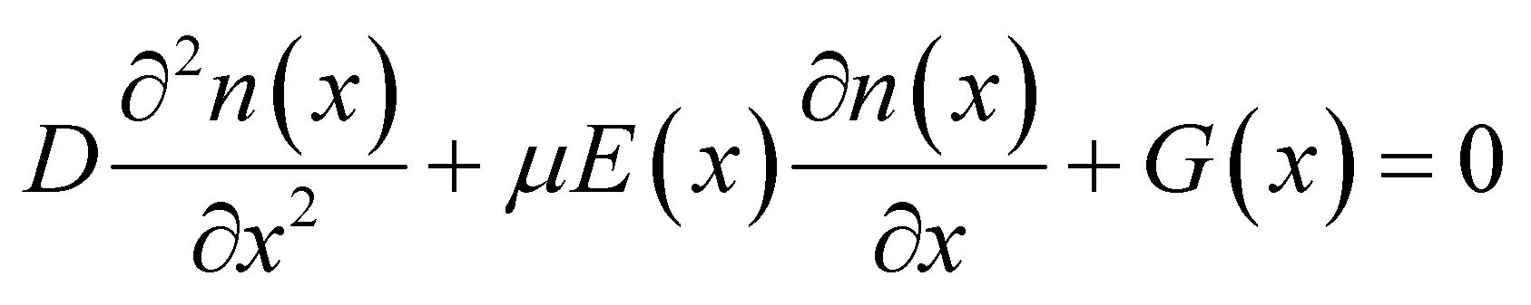 | (1) |
 | (2) |
Then the detailed current–voltage characteristics can be expressed as:
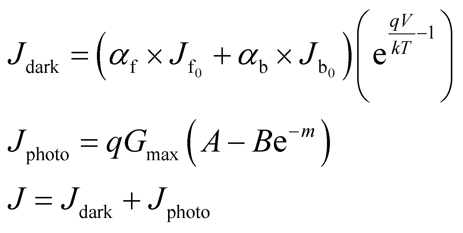 | (3) |
Based on piezo-phototronic theory, the current density of piezo-phototronic solar cell is given by:
 | (4) |
The open circuit voltage can be expressed as:
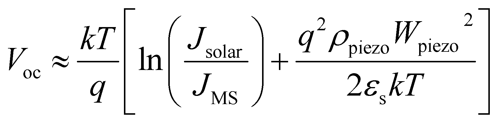 | (5) |
 | (6) |
In solar cell physics, the fill factor is the ratio of the maximum output power to the product of open circuit voltage and short circuit current, and can be obtained by:
 | (7) |
Fill factor can be influenced when the generation of charges changes significantly between open-circuit and short-circuit conditions. In the classical drift-diffusion model, recombination process which depends on a complex interplay between the effects of thickness,26 charge transport, recombination strength and light intensity plays an important role in the loss of photo-generated pairs.27 However, the extraordinarily long diffusion length25 in perovskite materials is larger than the active layer, thus the effect of recombination is neglected in this work.
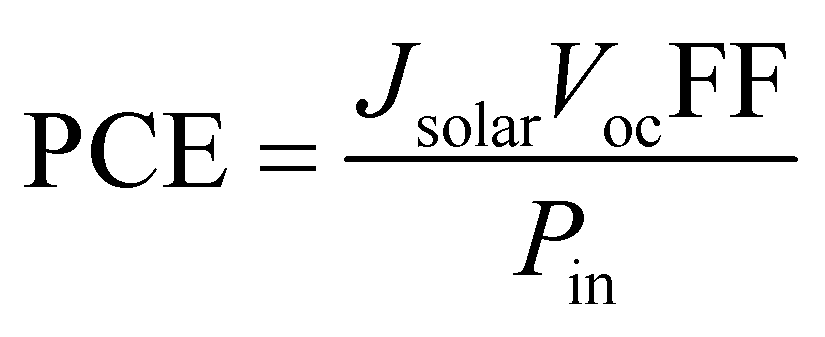
The power conversion efficiency (PCE) is the ratio of maximum output power to the total incident power, which can evaluate the overall efficiency of the solar cell. The PCE can be obtained as:
 | (8) |
3. Results and discussion
Typical parameters and coefficients are used to calculate the open circuit voltage, maximum output power, power efficiency, and fill factor. The temperature is set to 300 K, the width of piezo-charges distribution Wpiezo is 54.3 nm,28 the relative dielectric constant is 32. The piezoelectric constant of polar configuration of single crystal CH3NH3PbI3 which has molecular dipoles aligned preferentially along c-axis while distributed isotopically within the ab plane is used in the calculation and the piezoelectric constant along c-axis for CH3NH3PbI3 is 0.83 C m−2.20Fig. 2(a) presents the calculation model. A layer of CH3NH3PbI3 is sandwiched between upper HTM and bottom TiO2 composite layer. The J–V characteristics of the PPSC with externally applied strain ranging from −1% to 1% at a short circuit current density of 14 mA cm−2 is shown in Fig. 2(b). Fig. 2(c) shows the relation between the output power and voltage, which means the current density increases proportionally to applied strains, and peaks at Vm. By solving the above equations, the Voc and Pm as a linear function of the strain are shown respectively in the Fig. 2(d). The introduction of the piezo-phototronic effect improves the performance of the PPSC evidenced by the increased Vm and Pm.
 | ||
| Fig. 2 (a) Schematic of a PPSC with CH3NH3PbI3 thin film sandwiched between CuI and TiO2. (b) Relative current density varying with voltage when applied compressive strains ranging from −0.9% to 0.9% applied. (c) Output power of a PPSC as a function of voltage with various strains applied. (d) Maximum output power and open-circuit voltage under various compressive strains. | ||
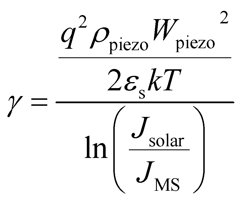
The modulation ratio γ of PPSC in relation to Wpiezo and strain ε is shown in Fig. 3(a). When Wpiezo increases from 48 nm at −1.0% compressive strain to 55 nm at 1.0% tensile strain, the ratio γ varies from −1.56% to 1.79%. While an external strain is applied in the CH3NH3PbI3 layer, the performance of the PPSC improves linearly. Fig. 3(b) is the γ as a function of strain when Jsolar is 14 mA cm−2 and 15.9 mA cm−2.29 The modulation ratio γ increases with the width of piezo-charge distribution Wpiezo, as illustrated in Fig. 3(c). Fig. 3(d) presents that the ratio γ as a function of the applied strain for two different piezoelectric perovskite materials: CH3NH3PbI3, BaTiO3. The piezoelectric constants for these two materials are 0.83 C m−2 (CH3NH3PbI3), 6.3 C m−2 (BaTiO3),30 respectively. The relative dielectric constants are 32 (CH3NH3PbI3), 600 (BaTiO3),31 respectively. Fig. 3(d) shows that the γ of CH3NH3PbI3 increases more significantly than that of BaTiO3 with strain varying from −1% to 1%. Though the piezoelectric constant e33 of BaTiO3 is much higher than that of the CH3NH3PbI3, the regulation ability is restricted because of its extremely high dielectric constant. Using the eqn (4) and eqn (5), FF and PCE, two parameters describing the performance of PSCs, are presented in Fig. 4(a) and (b) with the externally applied strain varying from −1% to 1%. Fill factor and power conversion efficiency of CH3NH3PbI3 piezo-phototronic solar cell are enhanced due to increasing maximum output power and open circuit voltage with the external strain applied.
 | ||
| Fig. 3 (a) The ratio γ of PPSC varies with γ and strain. (b) The ratio γ of PPSC increases with strain from −1% to 1% while Jsolar is 14 mA cm−2 and 15.9 mA cm−2. (c) The control ratio γ of PPSC as a function of Wpiezo with strains as 0.2%, 0.6% and 1% respectively. (d) The control ratio γ of PPSC changes with strain based on different perovskite materials: CH3NH3PbI3 and BATiO3. | ||
 | ||
| Fig. 4 (a) Fill factor and (b) power conversion efficiency of PPSC with strain ranging from −1% to 1%. | ||
4. Conclusion
In summary, the theoretical model of piezo-phototronic perovskite solar cells is presented and subsequently calculated in this paper. The open circuit voltage, maximum output power, fill factor and power efficiency are calculated and analyzed. Piezo-phototronic perovskite solar cells have enhanced performance under applied strains. Furthermore, compared to other piezoelectric materials, CH3NH3PbI3 demonstrates superior potential for applications in high-efficiency piezo-phototronic solar cells for its relatively high modulation factor and easier fabrication process. The theoretic results deepen the physical understanding of the piezo-phototronic perovskite solar cells and provide future guidance for the design of organic photovoltaic nanodevices.Conflicts of interest
There are no conflicts to declare.Acknowledgements
The authors are thankful for the support from University of Electronic Science and Technology of China (ZYGX2015KYQD063), Swansea University, SPARC II project, AgorIP project, the Innovate UK.References
- N. Banerji, Nat. Mater., 2017, 16(5), 503–505 CrossRef CAS PubMed.
- Y. Li, G. Xu, C. Cui and Y. Li, Adv. Energy Mater., 2017, 1701791 CrossRef.
- K. Leo, Organic photovoltaics, Nat. Rev. Mater., 2016, 1, 16056 CrossRef CAS.
- S. Albrecht and B. Rech, Nat. Energy, 2017, 2, 16196 CrossRef.
- G. E. Eperon, M. T. Hörantner and H. J. Snaith, Nat. Rev. Chem., 2017, 1, 0095 CrossRef.
- J. Huang, Y. Yuan, Y. Shao and Y. Yan, Nat. Rev. Mater., 2017, 2, 17042 CrossRef CAS.
- A. Kojima, K. Teshima, Y. Shirai and T. Miyasaka, J. Am. Chem. Soc., 2009, 131(17), 6050–6051 CrossRef CAS PubMed.
- Y. Yang and J. You, Nature, 2017, 544(7649), 155–156 CrossRef CAS PubMed.
- O. Ergen, S. M. Gilbert, T. Pham, J. Turner Sally, Z. Tan Mark Tian, A. Worsley Marcus and A. Zettl, Nat. Mater., 2016, 16, 522 CrossRef PubMed.
- T. Jiang and W. Fu, RSC Adv., 2018, 8(11), 5897–5901 RSC.
- W. Wu and Z. L. Wang, Nat. Rev. Mater., 2016, 1, 16031 CrossRef CAS.
- K. Zhang, M. Peng, W. Wu, J. Guo, G. Gao, Y. Liu, J. Kou, R. Wen, Y. Lei, A. Yu, Y. Zhang, J. Zhai and Z. L. Wang, Mater. Horiz., 2017, 4(2), 274–280 RSC.
- H. Zou, X. Li, W. Peng, W. Wu, R. Yu, C. Wu, W. Ding, F. Hu, R. Liu, Y. Zi and Z. L. Wang, Adv. Mater., 2017, 29(29), 1701412 CrossRef PubMed.
- Z. L. Wang and J. Song, Science, 2006, 312(5771), 242 CrossRef CAS PubMed.
- Y. Zhang, Y. Yang and Z. L. Wang, Energy Environ. Sci., 2012, 5(5), 6850 CAS.
- D. Q. Zheng, Z. Zhao, R. Huang, J. Nie, L. Li and Y. Zhang, Nano Energy, 2017, 32, 448–453 CrossRef CAS.
- L. Zhu, L. Wang, C. Pan, L. Chen, F. Xue, B. Chen, L. Yang, L. Su and Z. L. Wang, ACS Nano, 2017, 11(2), 1894–1900 CrossRef CAS PubMed.
- L. Zhu, L. Wang, F. Xue, L. Chen, J. Fu, X. Feng, T. Li and Z. L. Wang, Adv. Sci., 2017, 4(1), 1600185 CrossRef PubMed.
- N. Rajamanickam, S. Kumari, V. K. Vendra, B. W. Lavery, J. Spurgeon, T. Druffel and M. K. Sunkara, Nanotechnology, 2016, 27(23), 235404 CrossRef PubMed.
- S. Liu, F. Zheng, I. Grinberg and A. M. Rappe, J. Phys. Chem. Lett., 2016, 7(8), 1460–1465 CrossRef CAS PubMed.
- R. Ding, X. Zhang, G. Chen, H. Wang, R. Kishor, J. Xiao, F. Gao, K. Zeng, X. Chen, X. W. Sun and Y. Zheng, Nano Energy, 2017, 37(Suppl C), 126–135 CrossRef CAS.
- S. M. Sze, Physics of Semiconductor Devices, Wiley, New York, 1981 Search PubMed.
- X. Sun, R. Asadpour, W. Nie, A. D. Mohite and M. A. Alam, IEEE Journal of Photovoltaics, 2015, 5(5), 1389–1394 CrossRef.
- V. Gonzalez-Pedro, E. J. Juarez-Perez, W.-S. Arsyad, E. M. Barea, F. Fabregat-Santiago, I. Mora-Sero and J. Bisquert, Nano Lett., 2014, 14(2), 888–893 CrossRef CAS PubMed.
- S. D. Stranks, G. E. Eperon, G. Grancini, C. Menelaou, M. J. P. Alcocer, T. Leijtens, L. M. Herz, A. Petrozza and H. J. Snaith, Science, 2013, 342(6156), 341 CrossRef CAS PubMed.
- T. Kirchartz, T. Agostinelli, M. Campoy-Quiles, W. Gong and J. Nelson, J. Phys. Chem. Lett., 2012, 3(23), 3470–3475 CrossRef CAS PubMed.
- D. Bartesaghi, C. Perez Idel, J. Kniepert, S. Roland, M. Turbiez, D. Neher and L. J. Koster, Nat. Commun., 2015, 6, 7083 CrossRef CAS PubMed.
- L. Wei, Z. Aihua, Z. Yan and W. Zhong Lin, Nanotechnology, 2016, 27(20), 205204 CrossRef PubMed.
- Y. Okamoto and Y. Suzuki, J. Phys. Chem. C, 2016, 120(26), 13995–14000 CAS.
- A. I. Lebedev, J. Adv. Dielectr., 2012, 02(01), 1250003 CrossRef.
- B. Bajac, J. Vukmirovic, D. Tripkovic, E. Djurdjic, J. Stanojev, Ž. Cvejic, B. Škoric and V. V. Srdic, Process. Appl. Ceram., 2014, 8(4), 219–224 CrossRef CAS.
Footnote |
| † These authors contributed equally to this work. |
| This journal is © The Royal Society of Chemistry 2018 |