
 Open Access Article
 This Open Access Article is licensed under a Creative Commons Attribution-Non Commercial 3.0 Unported Licence
Bistable electrical switching and nonvolatile memory effects by doping different amounts of GO in poly(9,9-dioctylfluorene-2,7-diyl)†
Ying Xina,
Xiaofeng Zhaob,
Xiankai Jianga,
Qun Yanga,
Jiahe Huanga,
Shuhong Wang *a,
Rongrong Zhenga,
Cheng Wang*ac and
Yanjun Houa
*a,
Rongrong Zhenga,
Cheng Wang*ac and
Yanjun Houa
aSchool of Chemical Engineering and Materials, Heilongjiang University, Harbin 150080, P. R. China. E-mail: openair@163.com
bSchool of Electronic Engineering, Heilongjiang University, Harbin 150080, P. R. China
cKey Laboratory of Functional Inorganic Material Chemistry, Heilongjiang University, Ministry of Education, Harbin 150080, P. R. China. E-mail: wangc_93@163.com
First published on 13th February 2018
Abstract
Poly(9,9-dioctylfluorene-2,7-diyl) (PFO) was synthesized under a Suzuki coupling reaction, and its structure was proved by Fourier transform infrared (FT-IR) spectroscopy, and hydrogen and carbon nuclear magnetic resonance (1H-NMR and 13C-NMR). A nonvolatile organic memristor, based on active layers of PFO and PFO:GO composite, was prepared by spin-coating and the influence of GO concentration on the electrical characteristics of the memristor was investigated. The results showed that the device had two kinds of conductance behavior: electric bistable nonvolatile flash memory behavior and conductor behavior. With an increase in GO concentration, the device has an increased ON/OFF current ratio, increasing from 2.1 × 101 to 1.9 × 10³, a lower threshold voltage (VSET), decreasing from −1.1 V to −0.7 V, and better stability. The current remained stable for 3 hours in both the ON state and OFF state, and the ON and OFF state current of the device did not change substantially after 9000 read cycles.
1. Introduction
Nowadays, organic resistive random access memory (ORRAM) materials are attracting widespread attention and may offer great advantages over storage devices in the future.1 In brief, a memory device is a nonlinear resistor with memory function. High resistance is defined as “1” and low resistance is defined as “0”, so we usually store data using the resistance. According to the literature, organic materials have many advantages, such as high scalability,2 high flexibility,3,4 low power consumption, low cost, good processability,5,6 and the possibility of molecular design by chemical methods.7–9 For the last few years, researchers have paid more attention to memristors and have focused on the doping of organic/carbon-based composites.10,11 Some ORRAM devices have been studied using different organic materials, such as poly(N-vinylcarbazole) (PVK),12 poly(vinyl phenol),13 poly(methyl methacrylate) (PMMA),14 polyimide (PI),15 triphenylamine (TPA),16 and so on. CNTs have been doped in organic materials, including poly(3,4-ethylenedioxythiophene):poly(styrenesulfonate), poly(3-hexyl-thiophene) (P3HT),17 PEDOT:PSS,18 and poly(vinyl alcohol) (PVA).19 In addition, GO can be added into memristors to obtain better physical and electronic properties, which can contribute to electronic applications and lead to potential applications in ORRAM devices.20–23In this work, we synthesized the conjugate polymer poly(9,9-dioctylfluorene-2,7-diyl) (PFO) via a Suzuki coupling reaction, and then prepared PFO:GO composites with different GO content. The PFO and PFO:GO composite films, as the electronic active layers, are sandwiched between indium-tin-oxide (ITO) anodes and Al cathodes, and then the ITO/PFO/Al and ITO/PFO:GO/Al resistive switching memristors are fabricated. The current–voltage (I–V) characteristic curves were measured with a semiconductor analyzer. The results show that the device doped with 1.64% GO content reached the maximum ON/OFF current ratio and a higher stability.
2. Experimental
2.1 Materials
Organic solvents and anhydrous sodium carbonate were purchased from Sinopharm Co. Ltd. The solvents used in this work were purified, dried, and distilled in dry nitrogen. 9,9-dioctyl-2,7-dibromofluorene and 9,9-dioctylfluorene-2,7-diboronic acid bis(1,3-propanediol)ester were purchased from Sigma-Aldrich and used with no further purification. GO was prepared by the Hummers method from graphite powder, and dried for a week under vacuum.24 The TEM of GO is shown in Fig. 1(a); it is established from the image that the GO is multilayer.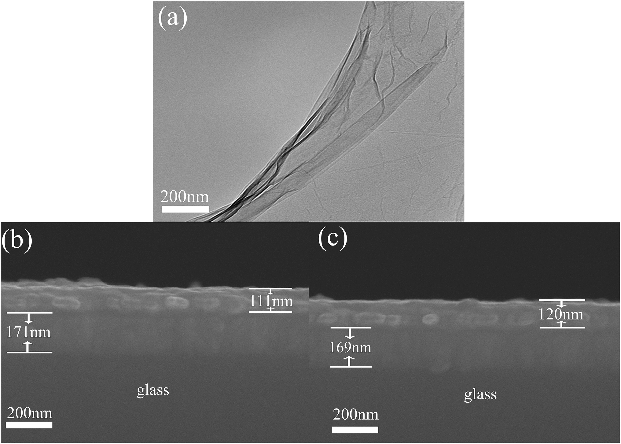 | ||
| Fig. 1 (a) TEM of GO, and cross-section scanning electron microscopic images of (b) ITO/PFO/Al and (c) ITO/PFO:GO/Al. | ||
2.2 Synthesis of poly(9,9-dioctylfluorene-2,7-diyl) (PFO)
The conjugate polymer PFO was synthesized by the Suzuki method. Scheme 1 represents the synthetic route of the polymer. The experimental process is shown as follows: first, 9,9-dioctyl-2,7-dibromofluorene (0.4911 g, 0.8954 mmol) and 9,9-dioctylfluorene-2,7-diboronic acid bis(1,3-propanediol)ester (0.5000 g, 0.8954 mmol) were dissolved in 14 mL degassed toluene. Then, Pd(PPh3)4 (0.0310 g, 2.686 × 10⁻² mmol) and Na2CO3 solution (14 mL, 3.0 mol L−1) were added to a Schlenk flask. Next, the reaction mixture was stirred under a nitrogen atmosphere and heated slowly from 95 °C to 105 °C, and then maintained at 105 °C for 48 h. Then, after cooling to room temperature, the mixture was washed several times with deionized water, concentrated, distilled under reduced pressure, and then dropped into cold methanol with strong stirring in order to get the products. Next, the precipitate was extracted with acetone over 48 h in a Soxhlet apparatus and the remaining monomers and Pd catalysts were removed. The weight-average molecular weight (Mw) was 6.3 × 10⁴, determined by GPC.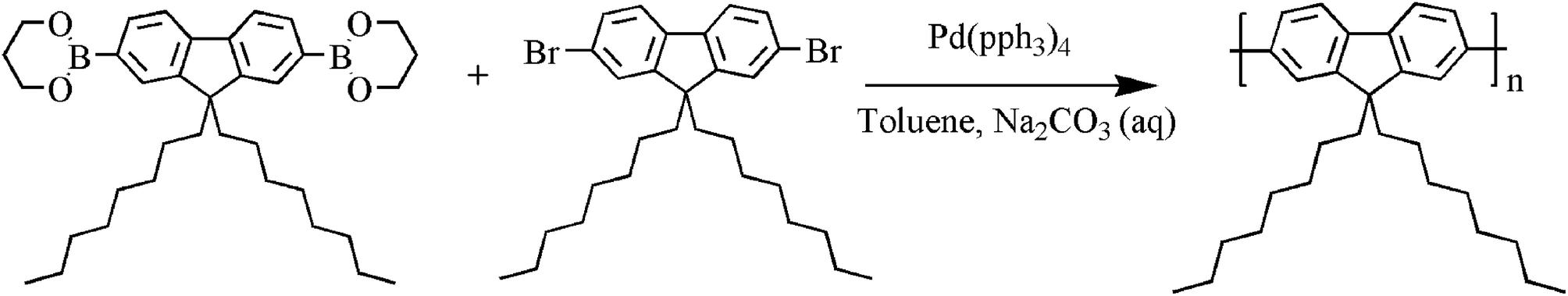 | ||
| Scheme 1 Synthesis route of PFO. | ||
FTIR spectra of PFO were obtained using Magna-IR560 infrared spectrometers, as shown in Fig. S1.† The stretching of C–H bonds in octyl produces a characteristic absorption peak at 2925 cm−1 and the stretching of C![[double bond, length as m-dash]](https://www.rsc.org/images/entities/char_e001.gif) C bonds is indicated at 1457 cm−1. The peak at 812 cm−1 can be attributed to the Ar-H stretching vibration.
C bonds is indicated at 1457 cm−1. The peak at 812 cm−1 can be attributed to the Ar-H stretching vibration.
Fig. S2† shows the 1H-NMR of PFO. 1H-NMR (400 MHz, CDCl3) δH (ppm): 0.79–0.82 (6H, m, J = 18 Hz), 1.13 (24H, m), 2.12 (4H, s), 7.67–7.70 (4H, m, J = 18 Hz), 7.82–7.84 (2H, d, J = 12 Hz).
The 13C-NMR of PFO is shown in Fig. S3.† 13C-NMR (100 MHz, CDCl3), δC (ppm): 151.83, 140.53, 140.04, 126.18, 121.25, 119.89, 31.81, 30.06, 29.24, 27.06, 24.49, 22.61, 17.87, 14.07, 9.32.
2.3 Fabrication and measurement of the memristor
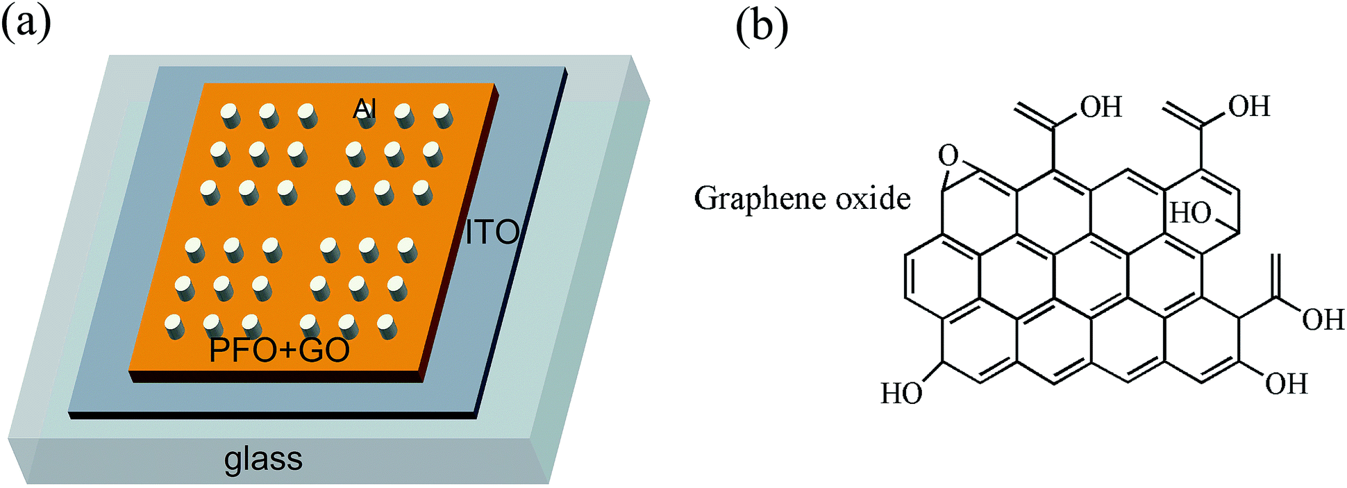 | ||
| Fig. 2 (a) Schematic of the ITO/PFO:GO/Al device; (b) the chemical structure of GO. | ||
Before fabricating the devices, 2 cm × 1 cm of ITO conductive glass (sheet resistance Rs = 6–9 Ω □−1) was pretreated sequentially with the detergent, deionized water, acetone, isopropanol, and methanol in an ultrasonic bath for 40 min, and dried in a vacuum oven at 60 °C overnight.
| Sample | GO content in ethanol solution (mg mL−1) | Volume of GO solution (mL) | Volume of PFO toluene solution (3 mg mL−1) (mL) | GO content in the composite film (%) |
|---|---|---|---|---|
| A | 0.03 | 1 | 1 | 0.99 |
| B | 0.05 | 1 | 1 | 1.64 |
| C | 0.10 | 1 | 1 | 3.23 |
| D | 0.30 | 1 | 1 | 9.10 |
3. Results and discussion
3.1 SEM of PFO and PFO:GO films
Fig. 1 represents the SEM images of PFO and PFO:GO. As shown in Fig. 1(b), the PFO composite film, ITO film, and glass are displayed from the top to bottom, respectively, and the PFO:GO composite film, ITO film, and glass are shown in Fig. 1(c). The thickness of the composite film can be seen from 120 nm to 130 nm.3.2 Characteristics of the ITO/PFO/Al memristor
 | ||
| Fig. 3 (a) I–V curves and (b) the relationship between the ON/OFF ratio of the current and the applied voltage for the ITO/PFO/Al device. | ||
As shown in Fig. 4(a), when the voltage was 2 V, the stability of the device was measured and the results showed that there are no significant changes to both the ON state and OFF state across at least 3 h. Whether it is in the ON state or OFF state, the cycle numbers of the device were measured at 2 V pulses (pulse period = 2 ms, pulse width = 1 ms); the current did not change substantially after about 9000 read cycles, as shown in Fig. 4(b), which indicates that the memristor has excellent stability.
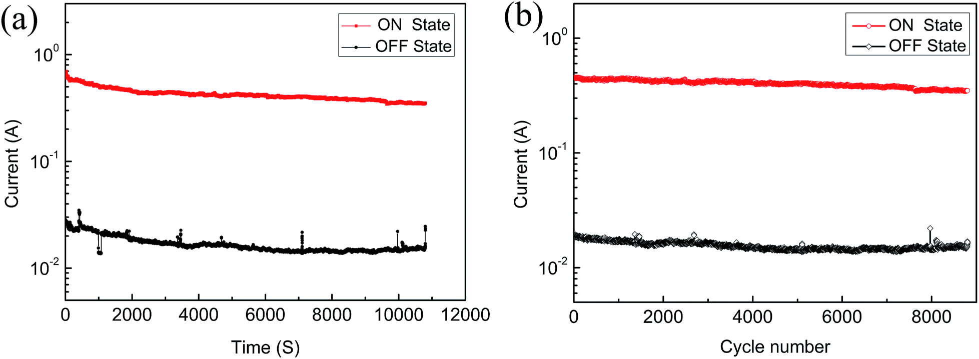 | ||
| Fig. 4 (a) Retention performance and (b) stimulus effect of read pulses on the ON and OFF states of the ITO/PFO/Al device. | ||
3.3 Characteristics of the ITO/PFO:GO/Al memristor
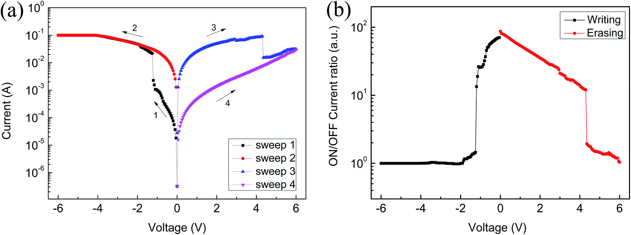
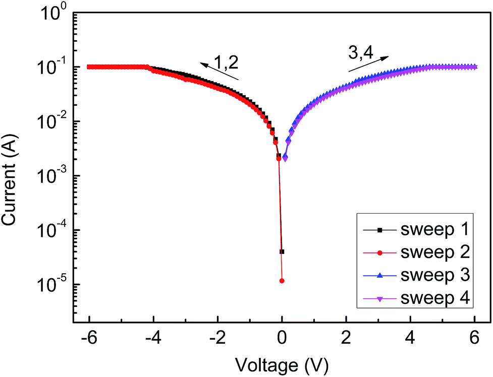
In order to assess the effect of GO on memristor performance, we doped different concentrations of GO in the PFO toluene solution; the specific ratios are shown in the Table 1. Compared to the ITO/PFO/Al device, ITO/PFO:GO/Al presents the same storage memory characteristics. At the same time, the ON/OFF current ratio and stability exhibit an obvious improvement. Furthermore, with an increase in the GO content, the ON/OFF current ratio increases significantly and it reaches a maximum value when the GO content is 1.64%. Notably, devices with a high concentration of GO (9.10%) exhibit conductor behavior only.Fig. 5 represents the I–V curve of the ITO/PFO:GO/Al device based on sample A. Fig. 5(a) shows the typical bistable electrical characteristics. The current abruptly rises from 4.1 × 10⁻⁴ A to 1.0 × 10⁻² A near −1 V. At this moment, the device switches from the OFF state to the ON state and remains in this state (sweep 2). However, the current drops suddenly from 8.5 × 10⁻² A to 2.2 × 10⁻² A near 4.2 V, and it returns to the OFF state. This is a typical flash memory device. As shown in Fig. 5(b), the ON/OFF current ratio increases after doping with GO, indicating that the rate of misreading is correspondingly reduced. The device was assessed at a voltage of 2 V at room temperature for 3 h (Fig. 5(c)). During this period, the current was maintained, which shows that the device has good stability. Fig. 5(d) reveals the cycle numbers of the sample A device; the current does not significantly change.
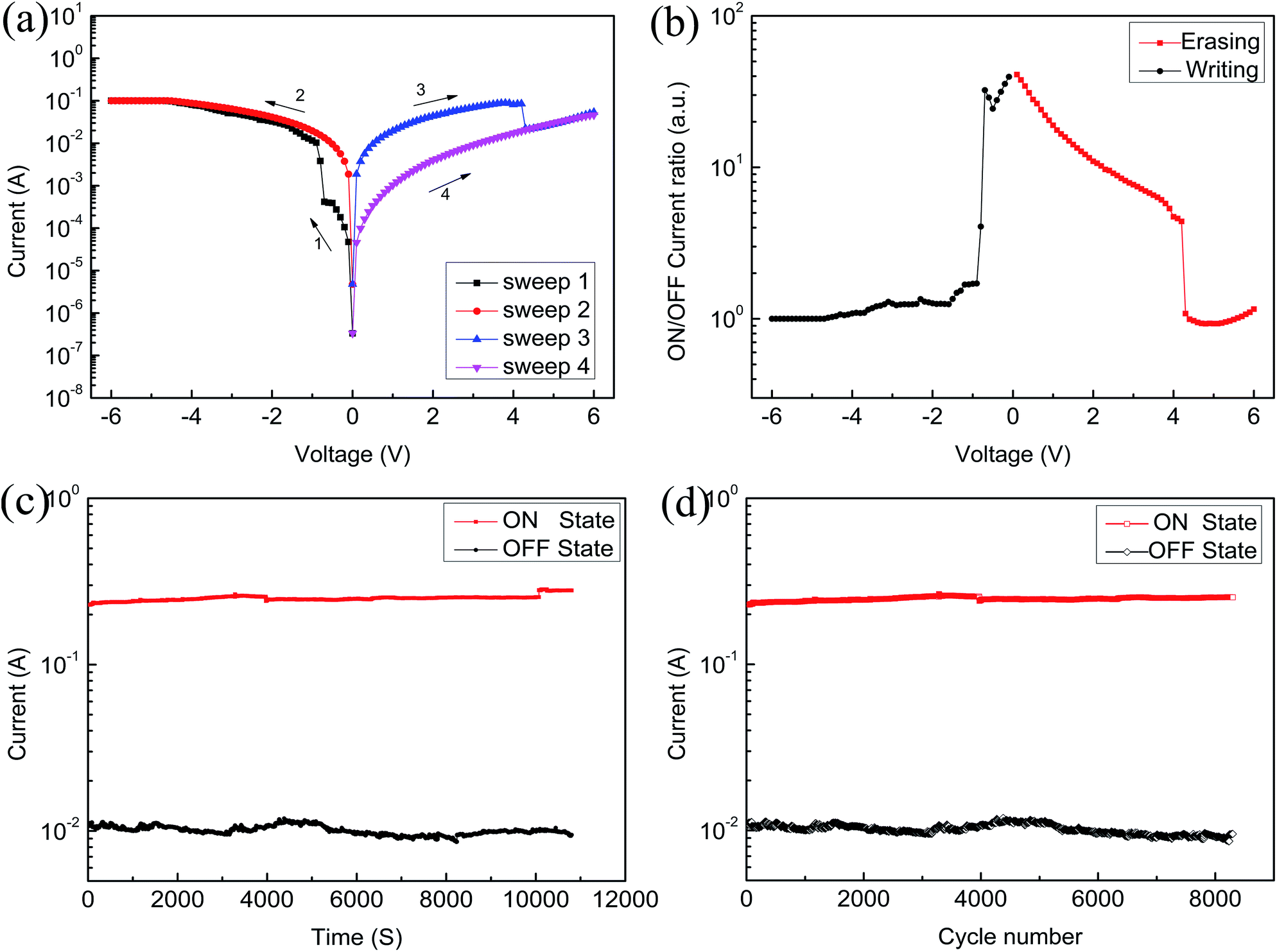 | ||
| Fig. 5 (a) I–V curves, (b) the relationship between the ON/OFF ratio of current and the applied voltage, (c) the retention performance, and (d) the stimulus effect of read pulses on the ON and OFF states of the ITO/PFO:GO/Al device based on sample A. | ||
As shown in Fig. 6 and 7, the devices based on sample B and sample C exhibit similar electrical bistable and nonvolatile flash memory characteristics. The current in the ON state increases with increasing GO concentration, which will be helpful in reducing the possibility of misreading. From Fig. 6(a), it is easy to discern that the threshold voltage has been reduced, which means that the device needs to overcome a smaller barrier from the OFF state to the ON state, and it also explains that the device has good reliability and low power consumption. Fig. 6(b) shows that the device presents a higher ON/OFF current ratio, increasing from 1.3 to 1900, from −6 V to 6 V. Fig. 6(c) shows that the device has been assessed at 2 V for 3 h and the current has no obvious degradation. Fig. 6(d) reveals the cycle numbers of the device (sample B) in the ON state and OFF state, which indicates that it has good stability.
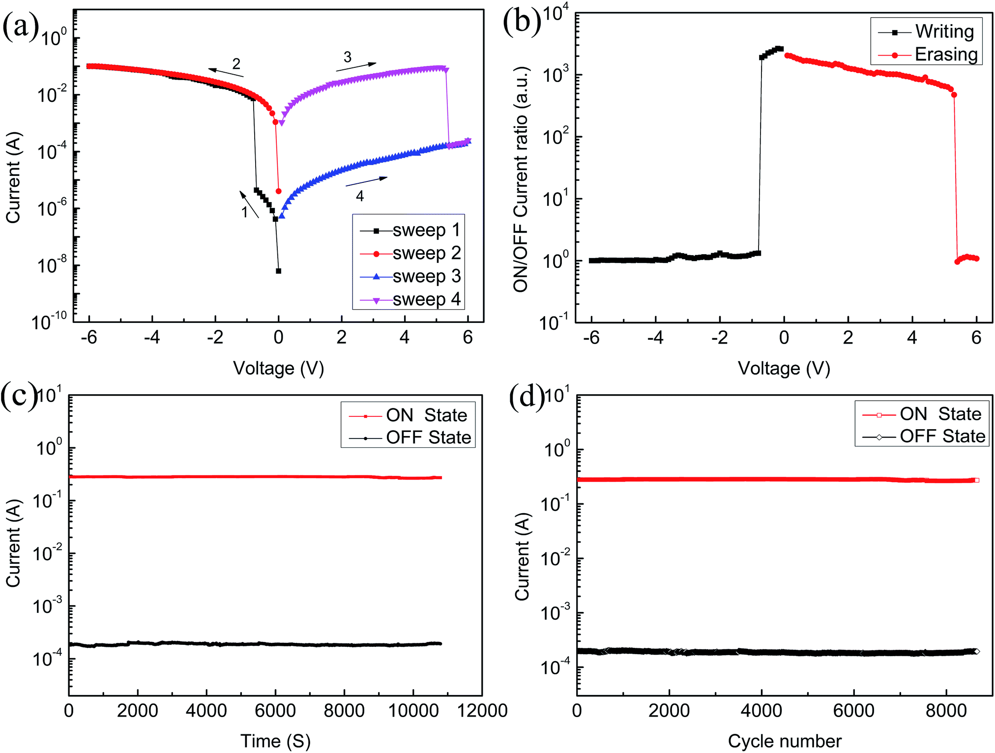 | ||
| Fig. 6 (a) I–V curves, (b) the relationship between the ON/OFF ratio of current and the applied voltage, (c) the retention performance, and (d) the stimulus effect of read pulses on the ON and OFF states of the ITO/PFO:GO/Al device based on sample B. | ||
Fig. 7(a) shows that the current gradually increases for sample C, but it is about an order of magnitude lower than for sample B. The ON/OFF current ratio of the device based on sample C increases from 1.5 to 247 when the voltage changes from −6 V to 6 V (Fig. 7(b)). Fig. 7(c) reveals that the retention properties of the device remain stable, which meets the requirement of a memory device. Fig. 7(d) reveals that the device in the ON and OFF states has good stability.
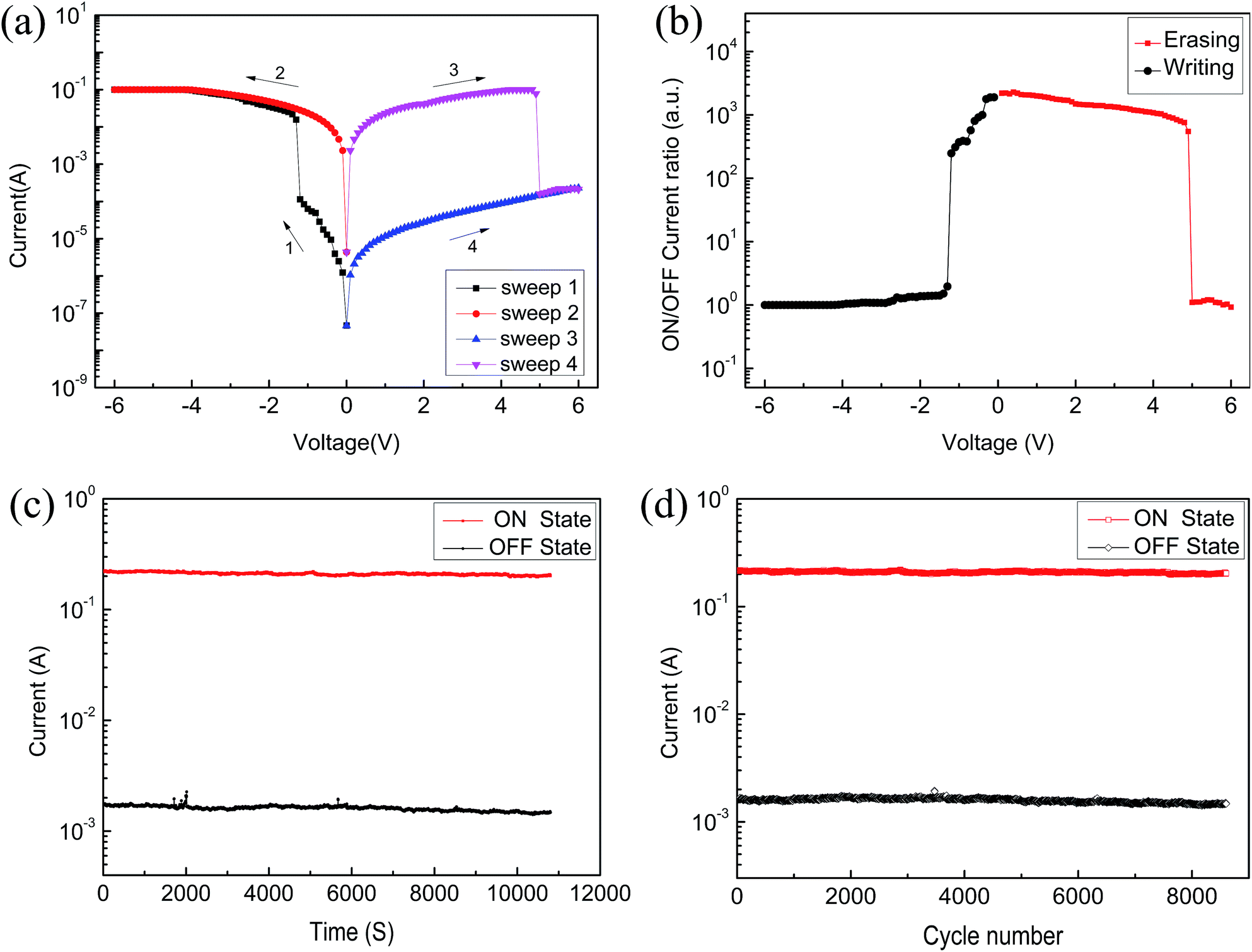 | ||
| Fig. 7 (a) I–V curves, (b) the relationship between the ON/OFF ratio of the current and the applied voltage, (c) the retention performance, and (d) the stimulus effect of read pulses on the ON and OFF states of the ITO/PFO:GO/Al device based on sample C. | ||
However, the device based on sample D represents completely different memory behavior. Fig. 8 reveals conductor behavior only.
 | ||
| Fig. 8 I–V curves of the ITO/PFO:GO/Al device based on sample D. | ||
The threshold voltage of the memory device has been reduced after doping with GO, mainly because of a higher GO content and shorter distance between the isolated GO, which reduces activation energy; the barrier that the device needs to overcome is also reduced. Through a series of tests, we found that the ON/OFF current ratio of the polymer film doped with GO was much higher (over 2 orders of magnitude) than that of previously reported films.25 In addition, the stability is also better, which greatly reduces the misreading rate of the device.20
3.4 Switching mechanism of the ITO/PFO:GO/Al device
In order to prove the switching mechanism of the memristor, we have investigated the I–V curve of the reset state using log–log plotting and linear fitting. Fig. 9 reveals that the ON states of the devices based on samples A, B and C have slopes of 1.08, 1.15, and 0.99 (nearly 1), respectively. This indicates a linear relationship between the current and the voltage, which is in accordance with Ohm’s law (I ∝ V). For the high resistance states of all the devices, similar ohmic conduction is formed at low voltages (sample A <0.5 V, sample B <1 V, and sample C <1.3 V), and the slopes for the devices are 1.18, 1.13, and 1.09, respectively. When the devices are at high voltage, the respective slopes for the devices are 2.02, 1.93, and 1.94 for the reset process (nearly 2). This illustrates that the relationship between current and voltage is in accordance with Child’s law (I ∝ V2).26–28 The above analysis shows that the devices conform to Ohm’s law at low voltages, but the devices are in accordance with Child’s law at high voltages. This is the space charge limited current (SCLC) mechanism.29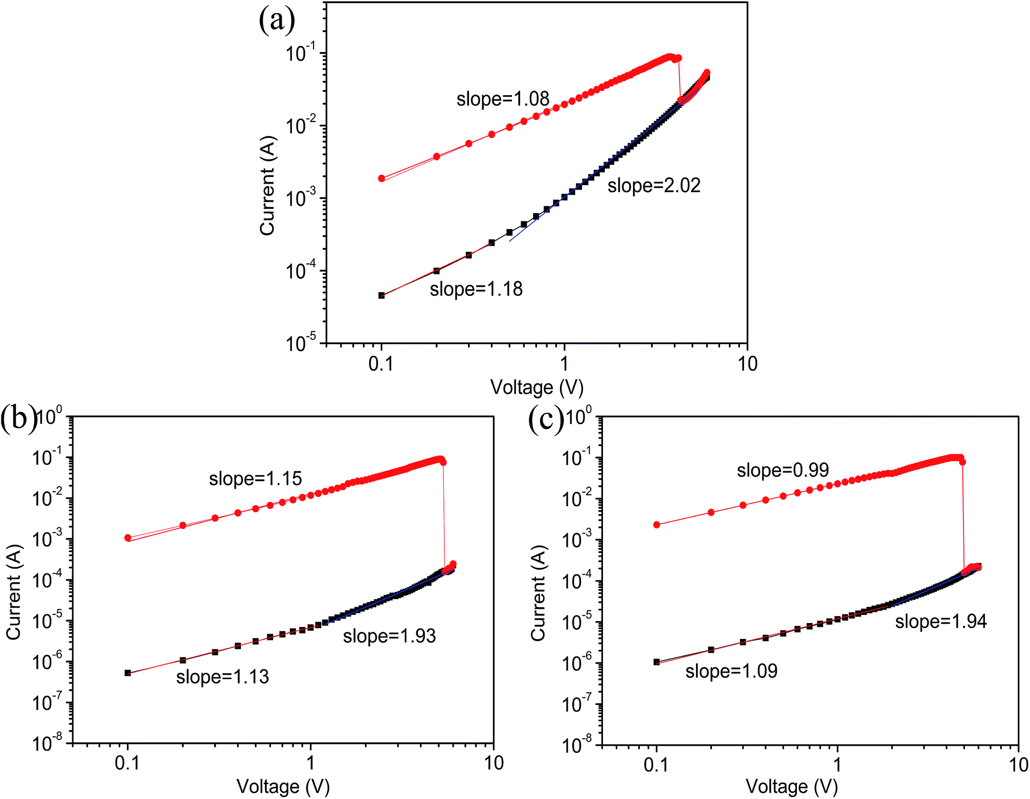 | ||
| Fig. 9 Linear fitting and corresponding slopes for the I–V curves of ITO/PFO:GO/Al devices based on (a) sample A, (b) sample B, and (c) sample C. | ||
For ITO/PFO:GO/Al devices, GO is randomly distributed in the polymer and plays a role in electron capture and transport. At low voltages, the electrons enter into the composite film from the Al electrode, where they are captured by GO and subsequently move constantly. As the voltage increases, the holes enter the device from the ITO. At this point, the charge carriers are trapped in the two electrodes and the composite films, and they form a space-charge layer. Consequently, other charge carriers are prevented from entering the composite membrane. However, when the threshold voltage is reached, most of the charge trapping centers change from unfilled to filled, and the current increases suddenly (writing process). Thereafter, a path is formed between the two electrodes, and the GO content has a significant effect on the device. As the GO concentration is increased, the valid distance between the isolated GO in the composite film becomes smaller – ultimately smaller than the diameter of separated GO. As a result, the amount of charge carriers increases rapidly throughout the composite film and the carriers can continuously jump between the two electrodes. Due to the distance getting closer, which can count against the carriers hopping, the ON/OFF state current ratio decreases.
In addition, the devices also generate a lot of heat. When the voltage is applied in the opposite direction, Joule heating breaks the original path, the current drops suddenly, and the device returns to the OFF state.30–32 This constitutes a cycle of write–read–erase–rewrite. Therefore, the device shows both bistable electrical switching and memory characteristics.
Owing to the fact that GO can capture more electrons at low voltage, when the scan voltage is increased to the threshold voltage, a large number of electrons enter the device, the current suddenly increases, and, at the same time, a conductive filament is formed. Therefore, the ON/OFF state current ratio of the device doped with GO is higher than that of the undoped device. However, when the GO content is much higher (9.10%), the device shows conductor behavior, mainly because the shorter distance between the isolated GO and the carriers forms a current pathway.
4. Conclusions
To sum up, we have successfully synthesized PFO via a Suzuki coupling reaction, and assembled memory devices with PFO and PFO:GO composites containing different GO content as active layers. The results show that memory devices present electrical bistable characteristics and nonvolatile flash behavior. With increasing GO concentration, the ON/OFF current ratio increases gradually from 2.1 × 101 to 1.9 × 10³ – the maximum ON/OFF current ratio of a device with 1.64% GO content was 1.9 × 10³ – and the threshold voltage decreases from −1.1 V to −0.9 V. The memory devices have better stability, which was measured continuously at 2 V for 3 h and the current had no obvious degradation. The mechanism of the memristors is the SCLC mechanism and the memory devices will contribute to digital storage in the future.Conflicts of interest
There are no conflicts of interest to declare.Acknowledgements
The authors are grateful for the support of the National Science Foundation of China (grant numbers 51527804, 51473056, 51503058, 51573015, 61471159), the Post-graduate Innovative Research Program of Heilongjiang University (grant number YJSCX2015-080HLJU), and the Natural Science Foundation of Heilongjiang Province of China (grant number B2017010).Notes and references
- Y. G. Ko, D. M. Kim, K. Kim, S. Jung, D. Wi, T. Michinobu and M. Ree, ACS Appl. Mater. Interfaces, 2014, 6, 8415 CAS.
- Z. S. Wang, F. Zeng, J. Yang, C. Chen and F. Pan, ACS Appl. Mater. Interfaces, 2012, 4, 447 CAS.
- Y. Sun, B. W. Wang, P. X. Hou, C. Liu, L. L. Fang, J. Tan, D. M. Sun and H. M. Cheng, Carbon, 2017, 124, 700 CrossRef CAS.
- D. Y. Yun, H. M. Park, S. W. Kim, S. W. Kim and T. W. Kim, Carbon, 2014, 75, 244 CrossRef CAS.
- S. L. Lim, Q. Ling, E. Y. H. Teo, C. X. Zhu, D. S. H. Chan, E. T. Kang and K. G. Neoh, Chem. Mater., 2017, 19, 5148 CrossRef.
- T. Kurosawa, T. Higashihara and M. Ueda, Polym. Chem., 2013, 4, 16 RSC.
- Y. Ma, P. Y. Gu, F. Zhou, H. L. Dong, Y. Y. Li, Q. F. Xu, J. M. Lu and W. L. Ma, RSC Adv., 2015, 5, 7083 RSC.
- Q. J. Zhang, H. Zhuang, J. H. He, S. G. Xia, H. Li, N. J. Li, Q. F. Xu and J. M. Lu, J. Mater. Chem. C, 2015, 3, 6778 RSC.
- Y. W. Liu, Y. Zhang, Q. Lan, S. W. Liu, Z. X. Qin, L. H. Chen, C. Y Zhao, Z. G. Chi, J. R. Xu and J. Economy, Chem. Mater., 2012, 24, 1212 CrossRef CAS.
- S. ChandraKishore and A. Pandurangan, RSC Adv., 2014, 4, 9905 RSC.
- Y. Liu, F. S. Li, Z. X. Chen, T. L. Guo, C. X. Wu and T. W. Kim, Vacuum, 2016, 130, 109 CrossRef CAS.
- A. Suresh, G. Krishnakumar and M. A. G. Namboothiry, Phys. Chem. Chem. Phys., 2014, 16, 13074 RSC.
- M. A. Mamo, A. O. Sustaita, N. J. Coville and I. A. Hümmelgen, Org. Electron., 2013, 14, 175 CrossRef CAS.
- D. I. Son, T. W. Kim, J. H. Shim, J. H. Jung, D. U. Lee, J. M. Lee, W. I. Park and W. K. Choi, Nano Lett., 2010, 10, 2441 CrossRef CAS PubMed.
- S. F. Miao, Y. X. Zhu, Q. Bao, H. Li, N. J. Li, S. J. Ji, Q. F. Xu, J. M. Lu and L. H. Wang, J. Phys. Chem. C, 2014, 118, 2154 CAS.
- D. Kim, S. Park, T. Lee, S. Hahm, K. Kim, J. Kim, W. Kwon and M. Ree, Langmuir, 2009, 25, 11713 CrossRef CAS PubMed.
- C. E. Cava, R. Possagno, M. C. Schnitzler, P. C. Roman, M. M. Oliveira, C. M. Lepiensky, A. J. G. Zarbin and L. S. Roman, Chem. Phys. Lett., 2007, 444, 304 CrossRef CAS.
- J. Ávila-Niño, W. Machado, A. Sustaita, E. Cardenas, M. Reyes, R. Sandoval and I. Hümmelgen, Org. Electron., 2012, 13, 2582 CrossRef.
- Y. M. Sun, J. G. Lu, C. P. Ai, D. Z. Wen and X. D. Bai, Org. Electron., 2016, 32, 7 CrossRef CAS.
- W. J. Yu, S. H. Chae, S. Y. Lee, D. L. Duong and Y. H. Lee, Adv. Mater., 2011, 23, 1889 CrossRef CAS PubMed.
- G. L. Li, G. Liu, M. Li, D. Wan, K. G. Neoh and E. T. Kang, J. Phys. Chem. C, 2010, 114, 12742 CAS.
- J. Q. Liu, Z. Y. Yin, X. H. Gao, F. Zhao, A. P. Lin, L. H. Xie, Q. L. Fan, F. Boey, H. Zhang and W. Huang, ACS Nano, 2010, 7, 3987 CrossRef PubMed.
- Y. M. Sun, L. Li, D. Z. Wen and X. D. bai, Org. Electron., 2015, 25, 283 CrossRef CAS.
- H. G. Jeon, Y. H. Huh, S. H. Yun, K. W. Kim, S. S. Lee, J. S. Lim, K. S. An and B. Park, J. Mater. Chem. C, 2014, 2, 2622 RSC.
- J. Q. Liu, Z. Y. Zeng, X. H. Cao, G. Lu, L. H. Wang, Q. L. Fan, W. Huang and H. Zhang, Small, 2012, 8, 3517 CrossRef CAS PubMed.
- Y. Q. Li, R. C. Fang, A. M. Zheng, Y. Y. Chu, X. Tao, H. H. Xu, S. J. Ding and Y. Z. Shen, J. Mater. Chem., 2011, 21, 15643 RSC.
- J. Q. Liu, Z. Y. Zeng, X. H. Cao, G. Lu, L. H. Wang, Q. L. Fan, W. Huang and H. Zhang, Small, 2012, 8, 3517 CrossRef CAS PubMed.
- L. Liang, K. Li, C. Xiao, S. J. Fan, J. Liu, W. S. Zhang, W. H. Xu, W. Tong, J. Y. Liao, Y. Y. Zhou, B. J. Ye and Y. Xie, J. Am. Chem. Soc., 2015, 137, 3102 CrossRef CAS PubMed.
- Y. C. Chang and Y. H. Wang, ACS Appl. Mater. Interfaces, 2014, 6, 5413 CAS.
- Y. M. Sun, J. G. Liu, C. P. Ai and D. Z. Wen, Phys. Chem. Chem. Phys., 2016, 18, 11341 RSC.
- W. B. Zhang, C. Wang, G. Liu, X. J. Zhu, X. X. Chen, L. Pan, H. W. Tan, W. H. Xue, Z. H. Ji, J. Wang, Y. Chen and R. W. Li, Chem. Commun., 2014, 50, 11856 RSC.
- Y. Q. Li, H. H. Xu, X. Tao, K. J. Qian, S. Fu, Y. Z. Shen and S. J. Ding, J. Mater. Chem., 2011, 21, 1810 RSC.
Footnote |
| † Electronic supplementary information (ESI) available. See DOI: 10.1039/c8ra00029h |
| This journal is © The Royal Society of Chemistry 2018 |