
 Open Access Article
 This Open Access Article is licensed under a Creative Commons Attribution-Non Commercial 3.0 Unported Licence
Compact TiO2 films with sandwiched Ag nanoparticles as electron-collecting layer in planar type perovskite solar cells: improvement in efficiency and stability†
Seid Yimer Abate abc,
Wen-Ti Wu*a,
Someshwar Pola*d and
Yu-Tai Tao*a
abc,
Wen-Ti Wu*a,
Someshwar Pola*d and
Yu-Tai Tao*a
aInstitute of Chemistry, Academia Sinica, Nankang, Taipei 115, Taiwan. E-mail: ytt@gate.sinica.edu.tw
bTaiwan International Graduate Program (TIGP), Sustainable Chemical Science and Technology (SCST), Academia Sinica, Taipei, Taiwan
cDepartment of Applied Chemistry, National Chiao Tung University, Hsinchu, Taiwan
dDepartment of Chemistry, Nizam College, Osmania University, Hyderabad, India
First published on 19th February 2018
Abstract
Fabrication of perovskite solar cells (PSCs) in a simple way with high efficiency and stability remains a challenge. In this study, silver nanoparticles (Ag NPs) were sandwiched between two compact TiO2 layers through a facile process of spin-coating an ethanolic AgNO3 solution, followed by thermal annealing. The presence of Ag NPs in the electron-transporting layer of TiO2 improved the light input to the device, the morphology of the perovskite film prepared on top, and eliminated leakage current. Photoluminescence and electron mobility studies revealed that the incorporation of Ag NPs in the ETL of the planar PSC device facilitated the electron–hole separation and promoted charge extraction and transport from perovskite to ETL. Hysteresis-free devices with incorporated Ag NPs gave a high average short-circuit current density (Jsc) of 22.91 ± 0.39 mA cm−2 and maximum power conversion efficiency of 17.25%. The devices also showed enhanced stability versus a control device without embedded Ag NPs. The possible reasons for the improvement are analyzed and discussed.
Introduction
One of the most challenging issues nowadays is getting sustainable, clean, and cheap energy sources because emissions from burning fossil fuels are widely recognized to be the cause of global warming and health problems. Solar energy is one of the most promising choices because of its abundance and being free of cost. It's the conversion of solar energy into electricity and its storage that are the primary tasks. Much progress has been made over the years through the developments in solar cells of various types in terms of their efficiency.1 Yet for commercialization of these technologies, further improvements in efficiency, stability, and cost-reduction are needed.Recently, perovskite materials are catching much attention of researchers for its potential application in solar cell.2 Perovskite absorbs visible light, with a low and tuneable band gap of ∼1.5 eV, high electron and hole mobility, which make it a good candidate as the active component in solar cells. Since the breakthrough report of Miyasaka et al. using perovskite as a visible light sensitizer for photoelectrochemical cells, giving 3.8% power conversion efficiency (PCE),3 various advances have been made in device architecture and fabrication process, and most recently a high PCE of 21.1% has been reached for the perovskite-based solar cell.2,4–13
To further push for higher efficiency and ultimate commercialization of this technology, optimization of each component in the device has been tried, such as electron transporting layer (ETL), hole transporting layer (HTL), and electrode, besides the light-absorbing perovskite layer. In terms of ETL, a layer of mesoporous TiO2 (mp-TiO2) together with the compact TiO2 (c-TiO2) layer is necessary to reach the high efficiency reported.14 Other metal oxides or metal-doped TiO2 have been reported to modulate the electron-collecting or electron-transporting properties of the ETL.15–29 Core–shell metallic nanoparticles (NPs) were also introduced in the meso-superstructure layer, with some improvements reported.30,31 Metallic nanoparticles were explored for their unique absorption properties in the visible and near-IR region, as well as the plasmonic properties.32 In particular, silver nanoparticles, Ag NPs, were incorporated in various ways in different layers of perovskite solar cells (PSCs) and beneficiary effects have been demonstrated.33–39 Nevertheless, these devices usually involved more complicated preparation procedures, with little elaboration of the detailed mechanism.
In this work, we report the use of Ag NPs-embedded c-TiO2 as ETL to improve the opto-electrical characteristics, charge extraction and transportation of planar PSCs with a device configuration of FTO/c-TiO2/Ag NPs/c-TiO2/perovskite (CH3NH3PbI3)/Spiro-OMeTAD/Ag. The sandwiched Ag NPs were formed by a simple and robust spin-coating of ethanolic AgNO3 solution on the c-TiO2 layer and later annealed at high temperature. It was shown that the incorporation of Ag NPs in the centre of c-TiO2 ETL layer promoted the formation of larger perovskite crystals with reduced grain boundaries, so that the electron trap density and the charge recombination pathways in the film were reduced. Also, the Ag NPs, with a specific amount, act as an electron scavenger and therefore electron-transporting nature of the TiO2 layer was improved in the PSCs.
Experimental
Chemicals and materials
FTO (7 Ω) was purchased from UNI-ONWARD Corp. Titanium diisopropoxide bis(acetylacetonate) solution (75% in 2-propanol) and AgNO3 (99.9999% trace metal basis) is obtained from Sigma-Aldrich. Perovskite precursors PbI2 (99.9985%) were obtained from Alfa Aesar. The CH3NH3I (98%) and Spiro-OMeTAD were purchased from Lumtec. Li-TFSI was obtained from ACROS. 4-tert-Butylpyridine (TBP) was acquired from Ak Scientific Inc, and Ag slug (4 mm × 6 mm 99.9999%) was from Gredmann.Experimental procedure
The FTO glass was cut into the size of 1.5 cm × 1.8 cm. A part of the FTO substrate (∼4 mm) was etched with zinc powder and 2 N HCl. Then the substrate was cleaned by sonication in DI water, acetone, and 2-propanol respectively for 20 min and then dried in a flow of N2 gas. The FTO substrate was treated by UV ozone for 30 min before device fabrication.A solution of titanium diisopropoxide bis(acetylacetonate) was prepared by dissolving 55 μL stock solution of (75% in 2-propanol) in 1 mL 1-butanol to make 0.15 M solution. Spin-coating of this solution in a three-stage procedure (see ESI†) on the FTO substrate gave the single-layered c-TiO2, double layered c-TiO2 or Ag-embedded c-TiO2. Double-layered c-TiO2 was prepared by another spin-coating of c-TiO2 on the single-layered TiO2. To prepare Ag-sandwiched c-TiO2, different concentrations of ethanolic AgNO3 solutions (with drops of DI water added to dissolve AgNO3) was spin-coated on the single layered c-TiO2 and annealed at 130 °C for 10 min, followed by one additional spin-coating of the c-TiO2 precursor on the Ag NP-covered c-TiO2. Finally, all of the ETL layers were sintered at 500 °C for 30 min. Before coating perovskite layer, the ETL substrates were treated by UV–ozone for 30 min to clean the surface.
The perovskite precursor solution was prepared by following a one-step deposition procedure reported in the literature.40 To a solution of DMSO (1 M) containing PbI2 (1 M) and CH3NH3I (1 M), DMF (600 mg) is added and stirred at room temperature for 60 min. The precursor solution was passed through a 0.22 μm PVDF filter and then spin-coated on c-TiO2/FTO substrate at 4000 rpm for 25 s. Diethyl ether was used to wash DMF away to give CH3NH3I·PbI2·DMSO adduct. At the end of the spinning process, transparent perovskite film formed, which was converted to a thick black film after annealing for 2 min at 65 °C and 5 min at 100 °C.
For HTM, 40 mg Spiro-OMeTAD was dissolved in 0.5 mL chlorobenzene and 14.5 μL TBP, 7.5 μL Li-TFSI, and 14.5 μL FK209 were added successively. The solution was spin-coated on top of perovskite surface. Finally, 70–80 nm thick Ag metal was deposited as the terminal contact by thermal deposition at a pressure of 8 × 10⁻⁶ torr in a metal-masked area of 0.04 cm2.
Characterization
The surface morphology and cross-section images of the devices were taken by field-emission scanning electron microscope (FE-SEM, ULTRA PLUS, a member of Carl Zeiss). Powder X-ray diffractions (XRDs) were recorded on a Bruker D8 Advance with Cu anode, λ = 1.54060 Å (angle range of 2θ = 10° to 45°). PANCHUM PR-2000 (M) UV/VIS spectrophotometer was used to measure the UV-Vis absorption spectra of the perovskite. Steady-state photoluminescence spectra (PL) were taken at room temperature by FL920 (FLSP920 Edinburgh Photonics model) fluorimeter. Kratos Axis Ultra DLD was employed to obtain X-ray Photoelectron Spectroscopy (XPS) spectra. Atomic force microscopy analyses were carried out with a Multimode Atomic Force Microscope (Digital Instruments, Nanoscope III) using tapping mode with a silicon tip. J–V characteristics of PSCs were measured by Keithley 2400 digital source meter, under AM 1.5 G solar irradiation at 100 mW cm−2 (Newport, JIS C891, IEC 60904-9, ASTM E927-05 Class AAA) under 1 sun illumination with a scan rate of 0.01 V s−1. The light intensity was determined by using a standard silicon photodiode (Hamamatsu S1133), calibrated by the National Renewable Energy Laboratory. The incident photon-to-current efficiency (IPCE) was measured by a system combining a xenon lamp, a monochromator, a chopper and a lock-in amplifier, together with a calibrated silicon photodetector. Both J–V and IPCE measurements were carried out at ambient condition without cell encapsulation on an area defined by a 0.04 cm2 metal mask.Results and discussion
The Ag NPs-embedded TiO2 ETL was prepared by spin-coating ethanolic AgNO3 solutions of different concentrations (1–20 mM) onto a pre-formed c-TiO2/FTO layer, followed by another layer of c-TiO2 layer and then annealed at 500 °C,41 as detailed in the experimental procedure. The evidence of formation of Ag NPs from AgNO3 within the TiO2 layer after annealing was provided by XPS, XRD, and UV-Vis absorption spectroscopy. In the XPS measurement as shown in Fig. 1a (the full spectrum is presented in Fig. S1, ESI†), the deconvolution of Ag 3d5/2 and 3d3/2 signals gave binding energies at 368.0 and 374.1 eV respectively, which are consistent with previously published data for Ag NPs.42 The powder XRD patterns for Ag NPs-embedded ETL (Fig. 1b) revealed diffraction peaks at 2θ values of 38.2°, 44.3°, 64.7° and 77.4°, corresponding to that for (111), (200), (220), and (311) planes, and suggest the formation of pure face-centered cubic Ag NPs, with no other phases present.43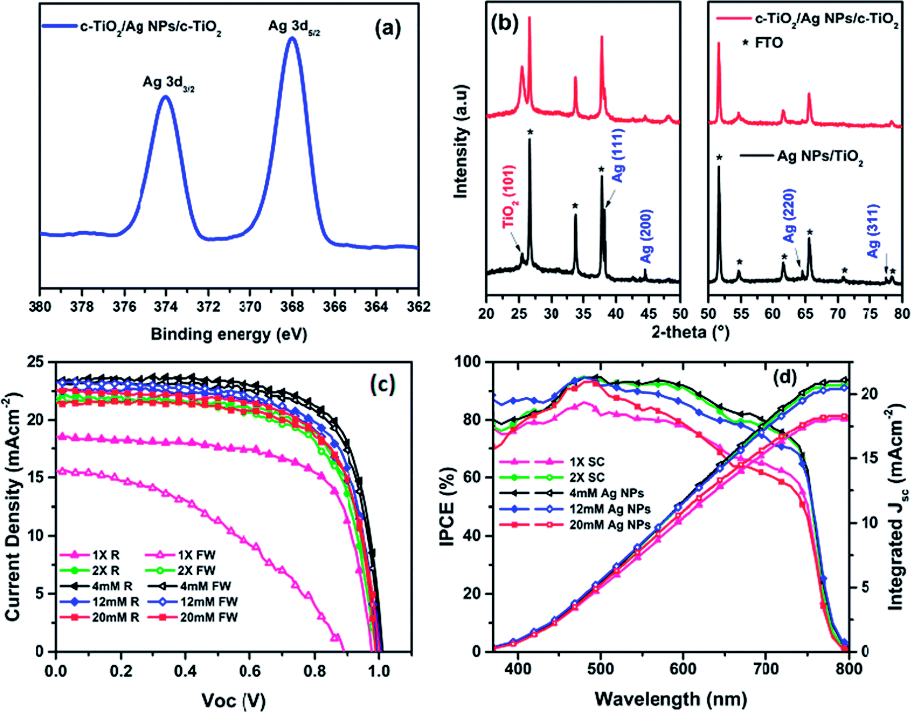 | ||
| Fig. 1 (a) XPS spectra of c-TiO2/Ag NPs (4 mM)/c-TiO2 prepared on FTO substrate (b) XRD of Ag NPs (4 mM)/c-TiO2 and c-TiO2/Ag NPs (4 mM)/c-TiO2 prepared on FTO, (c) reverse and forward sweep J–V characteristics (d) IPCE spectra and integrated Jsc of planar PSCs prepared form control and Ag NPs embedded ETLs. | ||
The UV-Vis absorption spectra (Fig. S2a, ESI†) revealed the absorption edge for pristine c-TiO2 shifted from 387 nm for the single layer c-TiO2 toward around 413 nm for the Ag NPs-embedded c-TiO2 layers, presumably due to the incorporation of Ag NPs, which is known to give UV absorption above 400 nm.37,44–46 Importantly, the TiO2 ETL embedding Ag NPs showed stronger UV-Vis absorption compared to the pristine c-TiO2, which may be the result of Surface Plasmon Resonance (SPR) of Ag NPs. All the aforementioned characterizations confirmed that Ag NPs were successfully formed in between the c-TiO2 layers. The optical transmittance of ETL is an important criterion to prepare high efficiency PSCs. So that, the optical transmittances are recorded for 1× SC, 2× SC and 4 mM Ag NPs-embedded TiO2 layers (Fig. S2b, ESI†). About 80% transmittance was recorded for all of the samples, which indicates that the incorporation of adequate amount Ag NPs insignificantly change the transmittance of the TiO2 film. With the Ag NPs in place, planar perovskite solar cells were then fabricated by spin-coating perovskite layer on top of various ETLs prepared under the same condition, followed by spin-coating Spiro-OMeTAD and depositing Ag back electrode to complete the device structure. A preliminary survey of the effect of incorporating Ag NPs on device performance was carried out, with the Ag NPs prepared from aqueous AgNO3 solutions of 1 mM to 20 mM concentrations. As a reference cell, TiO2 layers by spin-coating once and twice were also used. Abbreviations of 1× SC, 2× SC, 2× SC AgNO3 (x mM) are used to represent devices with single spin-coating, double spin-coating, and double spin-coating with embedded Ag NPs obtained from x mM AgNO3 solution respectively. The results showed that better performances were obtained with low concentration AgNO3 solutions and peaked for that from 4 mM AgNO3 solution.
Thus the device with 2× SC Ag NPs (4 mM) as ETL showed a maximum PCE of 17.25%, an open-circuit voltage (Voc) of 1.01 V, short-circuit current density (Jsc) of 23.36 mA cm−2, and a fill factor (FF) of 73.11% (Fig. 1c, Table 1). However, when 2× SC Ag NPs (12 mM, and 20 mM) were used as ETL, the device PCE decreased to 15.92% and 15.26% respectively with decreased Jsc and FF. In contrast, the reference solar cells fabricated by using 1× SC and 2× SC TiO2 as ETL showed smaller PCE than the 2× SC Ag NPs (4 mM) device, at 12.35% and 15.17% respectively. Compared to the others, the 1× SC device also had very low PCE for the forward sweep (5.80%), suggesting this device had substantial hysteresis, an undesirable situation in device operation. This phenomenon was eliminated for devices with TiO2 embedding Ag NPs, particularly for the 2× SC Ag NPs (4 mM) device (Table S1, ESI†).
| Method | Voc (V) | Jsc (mA cm−2) | FF (%) | PCE (%) | Rsh (KΩ cm−2) | Rs (Ω cm−2) |
|---|---|---|---|---|---|---|
| 1× SC | 0.95 ± 0.02 (0.98) | 16.76 ± 1.37 (18.47) | 68.90 ± 2.64 (68.20) | 11.02 ± 1.01 (12.35) | 0.35 | 6.27 |
| 2× SC | 0.99 ± 0.01 (0.98) | 21.79 ± 0.50 (21.95) | 69.33 ± 1.46 (70.51) | 14.91 ± 0.43 (15.17) | 1.67 | 4.76 |
| Ag NPs (4 mM) | 1.00 ± 0.01 (1.01) | 22.91 ± 0.39 (23.36) | 71.40 ± 1.81 (73.11) | 16.37 ± 0.32 (17.25) | 6.02 | 2.87 |
| Ag NPs (12 mM) | 0.99 ± 0.01 (0.99) | 22.40 ± 0.59 (22.52) | 67.82 ± 1.85 (71.41) | 15.03 ± 0.43 (15.92) | 3.12 | 3.34 |
| Ag NPs (20 mM) | 0.99 ± 0.01 (1.00) | 21.09 ± 1.06 (21.62) | 68.35 ± 2.54 (67.44) | 14.23 ± 0.68 (15.26) | 0.57 | 4.43 |
The PCE for the 2× SC device also improved over that for 1× SC device, to a maximum of 15.17%. This means ca. 23% improvement over the pristine 1× SC-based device. The possible reason for the improved performance could be a better c-TiO2 coverage on FTO layer when a second c-TiO2 layer was employed. This would reduce the possible direct contacts between perovskites and FTO, which is expected to decrease the chance of charge separation and increase recombination for the excited perovskites. However, 2× SC devices showed higher series resistance (Rs) and much smaller shunting resistance (Rsh), compared to the Ag NPs-incorporated PSCs. As shown in Table 1, the Rs for 2× SC (ca. 4.76 Ω cm−2) device is about two folds higher than that with 2× SC Ag NPs (4 mM) device (ca. 2.87 Ω cm−2). A higher Rs would suggest lower electron mobility for the device without Ag NPs-embedded, as will be discussed later. The same phenomena were observed for Rsh measurement, which quantifies explicitly the degree of recombination at the interface and relates to photocurrent loss.47 The device with 2× SC Ag NPs (4 mM) showed a Rsh value of 6020 Ω cm−2, which is more than three-fold photocurrent loss resistance than that with 2× SC (1670 Ω cm−2). This suggests that in the device fabricated with Ag NPs (4 mM) ETL, the photogenerated charge carriers are successfully separated and transported by suppressing charge recombination at the interfaces and resulting in a higher PCE. The Rs and Rsh properties were improved for nearly all of the Ag NPs-embedding devices compared to 1× SC and 2× SC devices, although when the amount of Ag NPs increased by using 12 mM and 20 mM solution, the series resistance started to build up and Rsh decreased to 3120 Ω cm−2 and 570 Ω cm−2 respectively, resulting in a decrease in performances of the cells. The box charts in Fig. 2 summarize the photovoltaics performance characteristics for devices prepared on various TiO2 substrates. Apparently, the highest Jsc values were recorded for devices prepared from that with 2× SC Ag NPs (4 mM) ETL, so were the PCEs for these devices. The histogram in Fig. S3, ESI† also showed the average PCE and their corresponding Voc, Jsc, FF for at least 15 devices each for 1× SC, 2× SC and 2× SC Ag NPs (4 mM)-based ETL and confirmed the high reproducibility of the performance characteristics. Thus there is ∼39% and ∼14% PCE enhancement for devices prepared from the 2× SC Ag NPs (4 mM)-based device over the pristine 1× SC and 2× SC respectively.
 | ||
| Fig. 2 Box chart comparison of photovoltaics parameters for 1× SC, 2× SC and Ag NPs (4 mM, 12 mM and 20 mM) ETL-based planar PSCs. | ||
That the incorporation of Ag NPs in the TiO2 layer has a beneficiary effect on the device performance is further confirmed by additional evidences as described below. The incident photon-to-current efficiency (IPCE) mainly depends on the average size of the perovskite crystals, grain boundaries, and perovskite thickness, which influence the light harvesting efficiency (ηlhe), exciton diffusion efficiency (ηed), charge separation efficiency (ηcs), and charge collection efficiency (ηcc).48 The IPCE of the control and Ag NPs-embedded cells are presented in Fig. 1d. It can be seen that Ag NPs (4 mM)-embedded device having the highest integrated Jsc gave a maximum IPCE% of ∼88% at ca. 495 nm and the highest IPCE% in the broad wavelength range from 450 nm to 750 nm compared to the other ETLs. However, the Ag NPs embedded ETL showed a little absorbance enhancement at about 450–600 nm, the IPCE improvement is all over the 400–800 nm range. As a result of incorporation of Ag NPs, the light absorption of perovskite increased not only in a specific region but also in all panchromatic wavelength ranges so that the IPCE is influenced accordingly. The same phenomena are observed when Ag and Au core shall metallic nanoparticles are incorporated in ETL of perovskite solar cell.30,31 The rather flat spectral profile and high IPCE% led to outstanding light harvesting efficiency. Whereas, the control device with 1× SC and 2× SC TiO2 showed ∼78% and 86% IPCE respectively at the same wavelength. When the amount of Ag NPs increased, the IPCE% decreased. Thus similar trend as the PCE results is followed for respective devices. The integrated Jsc value is presented in double Y axis figure for IPCE in Fig. 1d, and integrated Jsc values of 18.1 mA cm−2, 20.8 mA cm−2, 21.1 mA cm−2, 20.5 mA cm−2 and 18.1 mA cm−2 are extracted for 1× SC, 2× SC, 4 mM Ag NPs-, 12 mM Ag NPs- and 20 mM Ag NPs-incorporated TiO2 films respectively. A small discrepancy (∼2–9.6%) was observed between the Jsc measured from J–V and Jsc integrated from IPCE because the latter measurement was carried out in a single wavelength with much lower intensity than the one sun radiation.49,50
In order to understand the root cause for suppressed PCE when increasing Ag NPs concentration in the ETL, the top view SEM images for the perovskite films grown on respective ETLs were taken. As shown in Fig. 3a–c, the top-view SEM images of perovskite films on 1× SC, 2× SC, and Ag NPs (4 mM) ETLs are different in terms of surface morphology. Grains in the perovskite film grown on 2× SC Ag NPs (4 mM) TiO2 were bigger compared to that on 1× SC and 2× SC TiO2. The grains in films on 2× SC Ag NP (12 mM and 20 mM) had similar crystal size as for Ag NP (4 mM), but more cracks appeared, particularly for Ag NP (20 mM) (Fig. S4a and b, ESI†). It is intriguing that the Ag NPs buried within c-TiO2 layer would affect the morphology of perovskite deposited on top. Considering the surface energy of a substrate would affect the morphology of a film formed on top, we measured the water contact angle on various c-TiO2 surfaces (Fig. 3e–g). The same treatment of 30 min UV–ozone exposure was applied to all of the ETLs before measuring contact angles. The water contact angle value on 1× SC and 2× SC TiO2 had a value of <5°, which suggests a highly wettable surface. However, the water contact angle on Ag NPs (4 mM), Ag NPs (12 mM) and Ag NPs (20 mM) TiO2 increased to ∼10.5°, ∼15° and ∼22° respectively. These may suggest that a delicate dependence of grain size on the wettability, smaller and continuous grains for highly wettable surfaces and yet cracks appearing for less wettable surfaces. Previous reports on wettability of the solid surface showed that the roughness of a solid surface will have an effect on wetting property in that a rougher surface tend to be more wettable.51 Our AFM micrographs show that 1× SC has the highest roughness (26.1 nm) and it showed high wettability with a contact angle of less than 5°. The surface roughness decreased to 23.0 nm for 2× SC, and a lower surface roughness was observed for all Ag NPs-incorporated surfaces, with a least roughness of 20.7 nm for 4 mM Ag NPs-embedded film. The perovskite film coated on the rougher surface (thus more wettable surface) gave smaller grain size because of more nucleation sites present on the rougher surface. A smoother ETL will induce the growth of larger grains of perovskite layer.
 | ||
| Fig. 3 Top view SEM images of (a–c) perovskite films prepared on 1× SC, 2× SC and Ag NPs (4 mM) ETL, (d) cross-section SEM image of perovskite device with a structure of FTO/Ag NPs (4 mM)/perovskite/Spiro-OMeTAD/Ag, water contact angle (e–g) on 1× SC, Ag NPs (12 mM)- and Ag NPs (20 mM)-embedded TiO2 surfaces after 30 min UV–ozone treatment, (h–l) AFM surface and corresponding 3-dimentional images (bottom) of ETL films prepared from 1× SC, 2× SC, 4 mM Ag NPs, 12 mM Ag NPs and 20 mM Ag NPs respectively (all scans are 5 μm × 5 μm). | ||
The thickness of 1× SC, 2× SC and Ag NPs (4 mM) TiO2 were measured by cross-sectional SEM and the results are presented in (Fig. S4c and d, ESI† and Fig. 3d), with an ETL thickness of ∼50 nm, ∼90 nm, and ∼95 nm respectively. The perovskite layer thickness grown on different underneath layers were slightly different, at ∼340 nm, ∼350 nm, and ∼395 nm on 1× SC, 2× SC, and 2× SC Ag NPs (4 mM) TiO2 respectively. The top view and cross-sectional SEM micrographs suggested a certain level of roughness increased the thickness and improved the morphology of the perovskite film formed on top and contributed to the performance of the device recorded.52
UV-Vis and XRD were recorded for perovskite films grown on 1× SC, 2× SC and 2× SC Ag NPs (4 mM) ETL layers (Fig. S5a, ESI†). The active perovskite layer prepared in our process absorbed light in UV-Vis range with an absorption band edge ca. 770 nm, which is in agreement with the previous report.53 UV-Vis absorbing for Ag NPs (4 mM) showed a little improvement in the whole range of UV-Vis compared to 1× SC and 2× SC. The powder XRD spectra (Fig. S5b, ESI†) presented dominant peaks at 2θ of 14.2° (110) and 28.5° (220) for perovskite, with no traces for either PbI2 or CH3NH3I, indicating the formation of high quality and pure perovskite crystal over the ETLs. There is nevertheless little difference in the UV-Vis and PXRD results for perovskite on these c-TiO2 ETLs, probably because the amount of Ag NPs embedded is small.
Photoluminescence and electron mobility studies were carried out to understand the characteristics of charge separation and transportation in these devices. Thus the steady-state photoluminescence (PL) was measured on half devices of perovskite/ETLs/FTO with 1× SC, 2× SC and 2× SC Ag NPs (4 mM) TiO2 as ETL. As shown in Fig. 4, the PL spectrum of perovskite on a bare glass substrate showed a strong emission at ∼774 nm. Much reduced PL intensity was recorded for perovskite grown on 2× SC Ag NPs (4 mM) ETL. This presumably could indicate a suppressed charge recombination in the Ag NP-embedded film as compared to that on 1× SC and 2× SC ETL films. This suggests a higher chance of charge separation and transportation to the electrodes when the 2× SC Ag NP (4 mM) TiO2 is used as ETL. This is in agreement with the Rs and Rsh measurements of the prepared devices.
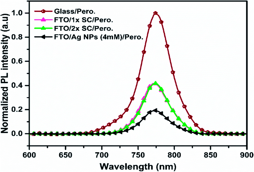 | ||
| Fig. 4 Normalized PL spectra of perovskite thin films prepared on glass, 1× SC ETL, 2× SC ETL and c-TiO2/Ag NPs (4 mM)/c-TiO2 ETLs. | ||
In order to confirm the influence of Ag NPs on charge carrier transport, electron-only device with a device configuration of FTO/c-TiO2/Ag NPs/c-TiO2/perovskite/Al (65 nm) was prepared, and the J–V characteristics were measured in the dark to determine electron mobility of the device. Mott–Gurney law is used to define Space-Charge-Limited Current (SCLC) region, with J = 9/8εoεrE2/L, where J is the current density, E is electric field, εo is permittivity of the vacuum (8.854 × 10⁻¹² F m−1), εr is the relative dielectric constant of CH3NH3PbI3 (εr = 32),54 and L is perovskite film thickness (1× ST = ∼330 nm, 2× SC = ∼350 nm and 2× SC Ag NP (4 mM) = ∼395 nm).14,45 The mobility is dependent on the electric field and can be expressed by a Poole–Frenkel equation μ(E) = μo![[thin space (1/6-em)]](https://www.rsc.org/images/entities/char_2009.gif) exp(βE1/2), where μo is the zero-field mobility and β is Poole–Frenkel factor. The slope (β) and intercept zero-field mobility (μo) were obtained from the plot of ln(JE−2) versus E1/2.55 The SCLC electron mobilities calculated are presented in Fig. 5. The device fabricated with Ag NPs (4 mM)-embedded TiO2 showed an electron mobility of 2.57 × 10⁻⁴ cm2 V−1 s−1, which is significantly higher than that with 1× SC (1.46 × 10⁻⁴ cm2 V−1 s−1) and 2× SC (2.03 × 10⁻⁴ cm2 V−1 s−1). This suggested the Ag NPs-incorporated ETL facilitated the charge extraction and prevent electron and hole recombination more than that with 1× SC and 2× SC ETLs. This also matched with the PL and charge resistance studies.
exp(βE1/2), where μo is the zero-field mobility and β is Poole–Frenkel factor. The slope (β) and intercept zero-field mobility (μo) were obtained from the plot of ln(JE−2) versus E1/2.55 The SCLC electron mobilities calculated are presented in Fig. 5. The device fabricated with Ag NPs (4 mM)-embedded TiO2 showed an electron mobility of 2.57 × 10⁻⁴ cm2 V−1 s−1, which is significantly higher than that with 1× SC (1.46 × 10⁻⁴ cm2 V−1 s−1) and 2× SC (2.03 × 10⁻⁴ cm2 V−1 s−1). This suggested the Ag NPs-incorporated ETL facilitated the charge extraction and prevent electron and hole recombination more than that with 1× SC and 2× SC ETLs. This also matched with the PL and charge resistance studies.
 | ||
| Fig. 5 Measurement of electron mobility by SCLC method at dark J–V characteristics for devices with and without the presence of Ag NPs. | ||
Finally, the long-term stability, which is one of the essential criteria for PSCs commercialization, was studied for devices with 1× SC, 2× SC and 2× SC Ag NPs (4 mM) as ETLs. Devices were stored in a dry box and only taken out for measurements in the atmosphere without encapsulation. The results are presented in Fig. 6, which revealed that PSC with 2× SC Ag NPs (4 mM) ETL retained ca. 89% of its initial PCE after 28 days, whereas that with 1× SC and 2× SC ETL degraded and retained ∼32% and ∼62% of their initial PCEs respectively after the same period. Also shown are the stability of other parameters like Voc, Jsc, and FF. The possible reason for better stability for Ag NPs (4 mM) may be the formation of bigger crystal with less grain boundaries so that the intrusion of moisture in the cell can be decreased.
 | ||
| Fig. 6 Long term stability test for 1× SC, 2× SC and Ag NPs (4 mM) ETL based-PSCs without encapsulation for 28 days. The dotted lines represent the maximum values for all device. The standard deviation in the normalized PCE box chart showed the average percentage retained at least for 5 devices. | ||
Conclusions
In summary, we demonstrated a new and cheaper approach to tune the ETL of the perovskite solar cell by incorporating Ag NPs inside the compact TiO2 layer through annealing AgNO3 salt deposited in the middle of the layer. Smooth and compact perovskite film was formed in the presence of Ag NPs, which improved the film morphology, electron extraction, and transport properties, as evidenced by SEM, PL and SCLC measurements. Higher electron mobility, Jsc, and FF, thus higher PCE were obtained when an adequate amount of Ag NPs was embedded in the TiO2 layer. Presumably, the growth of large crystals with fewer grain boundaries on Ag NPs-embedded ETLs improves the Jsc and FF of the device by suppressing series resistance and enhance shunting resistance and also contributed to the long-term stability for the prepared device.Conflicts of interest
There are no conflicts to declare.Acknowledgements
The authors wish to thank the financial support of Ministry of Science and Technology, Taiwan (Grant number: 106-2113-M-001-003) and SERB, India.Notes and references
- X. Fan, M. Zhang, X. Wang, F. Yang and X. Meng, J. Mater. Chem. A, 2013, 1, 8694 CAS.
- P. Gao, M. Grätzel and M. K. Nazeeruddin, Energy Environ. Sci., 2014, 7, 2448 CAS.
- A. Kojima, K. Teshima, Y. Shirai and T. Miyasaka, J. Am. Chem. Soc., 2009, 131, 6050 CrossRef CAS PubMed.
- M. Saliba, T. Matsui, J.-Y. Seo, K. Domanski, J.-P. Correa-Baena, M. K. Nazeeruddin, S. M. Zakeeruddin, W. Tress, A. Abate and A. Hagfeldt, Energy Environ. Sci., 2016, 9, 1989 CAS.
- N. J. Jeon, J. H. Noh, Y. C. Kim, W. S. Yang, S. Ryu and S. I. Seok, Nat. Mater., 2014, 13, 897 CrossRef CAS PubMed.
- J.-H. Im, I.-H. Jang, N. Pellet, M. Grätzel and N.-G. Park, Nat. Nanotechnol., 2014, 9, 927 CrossRef CAS PubMed.
- M. Liu, M. B. Johnston and H. J. Snaith, Nature, 2013, 501, 395 CrossRef CAS PubMed.
- Q. Chen, H. Zhou, Z. Hong, S. Luo, H.-S. Duan, H.-H. Wang, Y. Liu, G. Li and Y. Yang, J. Am. Chem. Soc., 2013, 136, 622 CrossRef PubMed.
- W. Nie, H. Tsai, R. Asadpour, J.-C. Blancon, A. J. Neukirch, G. Gupta, J. J. Crochet, M. Chhowalla, S. Tretiak and M. A. Alam, Science, 2015, 347, 522 CrossRef CAS PubMed.
- K. M. Boopathi, M. Ramesh, P. Perumal, Y.-C. Huang, C.-S. Tsao, Y.-F. Chen, C.-H. Lee and C.-W. Chu, J. Mater. Chem. A, 2015, 3, 9257 CAS.
- T. Salim, S. Sun, Y. Abe, A. Krishna, A. C. Grimsdale and Y. M. Lam, J. Mater. Chem. A, 2015, 3, 8943 CAS.
- T.-B. Song, Q. Chen, H. Zhou, C. Jiang, H.-H. Wang, Y. M. Yang, Y. Liu, J. You and Y. Yang, J. Mater. Chem. A, 2015, 3, 9032 CAS.
- G. Yang, H. Tao, P. Qin, W. Ke and G. Fang, J. Mater. Chem. A, 2016, 4, 3970 CAS.
- M. Abdi-Jalebi, M. I. Dar, A. Sadhanala, S. P. Senanayak, F. Giordano, S. M. Zakeeruddin, M. Grätzel and R. H. Friend, J. Phys. Chem. Lett., 2016, 7, 3264 CrossRef CAS PubMed.
- Q. Dong, Y. Shi, K. Wang, Y. Li, S. Wang, H. Zhang, Y. Xing, Y. Du, X. Bai and T. Ma, J. Phys. Chem. C, 2015, 119, 10212 CAS.
- Z. Zhu, X. Zheng, Y. Bai, T. Zhang, Z. Wang, S. Xiao and S. Yang, Phys. Chem. Chem. Phys., 2015, 17, 18265 RSC.
- M. A. Mejía Escobar, S. Pathak, J. Liu, H. J. Snaith and F. Jaramillo, ACS Appl. Mater. Interfaces, 2017, 9, 2342 Search PubMed.
- D. Bi, G. Boschloo, S. Schwarzmüller, L. Yang, E. M. Johansson and A. Hagfeldt, Nanoscale, 2013, 5, 11686 RSC.
- M. H. Kumar, N. Yantara, S. Dharani, M. Graetzel, S. Mhaisalkar, P. P. Boix and N. Mathews, Chem. Commun., 2013, 49, 11089 RSC.
- D.-Y. Son, J.-H. Im, H.-S. Kim and N.-G. Park, J. Phys. Chem. C, 2014, 118, 16567 CAS.
- M.-C. Wu, S.-H. Chan, M.-H. Jao and W.-F. Su, Sol. Energy Mater. Sol. Cells, 2016, 157, 447 CrossRef CAS.
- B. Zhao, X. Wen, M. Jiang, J. Wu, F. Lan, J. Wang, D. den Engelsen, G. Li and D. Gao, J. Mater. Chem. A, 2017, 5, 3691 CAS.
- X. Zhao, H. Shen, Y. Zhang, X. Li, X. Zhao, M. Tai, J. Li, J. Li, X. Li and H. Lin, ACS Appl. Mater. Interfaces, 2016, 8, 7826 CAS.
- D.-B. Li, L. Hu, Y. Xie, G. Niu, T. Liu, Y. Zhou, L. Gao, B. Yang and J. Tang, ACS Photonics, 2016, 3, 2122 CrossRef CAS.
- S.-G. Chen, S. Chappel, Y. Diamant and A. Zaban, Chem. Mater., 2001, 13, 4629 CrossRef CAS.
- M. Yang, R. Guo, K. Kadel, Y. Liu, K. O'Shea, R. Bone, X. Wang, J. He and W. Li, J. Mater. Chem. A, 2014, 2, 19616 CAS.
- D. H. Kim, G. S. Han, W. M. Seong, J. W. Lee, B. J. Kim, N. G. Park, K. S. Hong, S. Lee and H. S. Jung, ChemSusChem, 2015, 8, 2392 CrossRef CAS PubMed.
- F. Giordano, A. Abate, J. P. C. Baena, M. Saliba, T. Matsui, S. H. Im, S. M. Zakeeruddin, M. K. Nazeeruddin, A. Hagfeldt and M. Graetzel, Nat. Commun., 2016, 7, 10379 CrossRef CAS PubMed.
- J. Wang, M. Qin, H. Tao, W. Ke, Z. Chen, J. Wan, P. Qin, L. Xiong, H. Lei and H. Yu, Appl. Phys. Lett., 2015, 106, 121104 CrossRef.
- M. Saliba, W. Zhang, V. M. Burlakov, S. D. Stranks, Y. Sun, J. M. Ball, M. B. Johnston, A. Goriely, U. Wiesner and H. J. Snaith, Adv. Funct. Mater., 2015, 25, 5038 CrossRef CAS.
- W. Zhang, M. Saliba, S. D. Stranks, Y. Sun, X. Shi, U. Wiesner and H. J. Snaith, Nano Lett., 2013, 13, 4505 CrossRef CAS PubMed.
- P. Wang, D. Tanaka, S. Ryuzaki, S. Araki, K. Okamoto and K. Tamada, Appl. Phys. Lett., 2015, 107, 151601 CrossRef.
- Y. Liu, F. Lang, T. Dittrich, A. Steigert, C.-H. Fischer, T. Köhler, P. Plate, J. Rappich, M. C. Lux-Steiner and M. Schmid, RSC Adv., 2017, 7, 1206 RSC.
- D. Yang, J. G. Jang, J. Lim, J.-K. Lee, S. H. Kim and J.-I. Hong, ACS Appl. Mater. Interfaces, 2016, 8, 21522 CAS.
- G. Kakavelakis, K. Alexaki, E. Stratakis and E. Kymakis, RSC Adv., 2017, 7, 12998 RSC.
- J. Huang, M. Wang, L. Ding, F. Igbari and X. Yao, Sol. Energy, 2016, 130, 273 CrossRef CAS.
- H. Nourolahi, A. Behjat, S. H. Zarch and M. Bolorizadeh, Sol. Energy, 2016, 139, 475 CrossRef CAS.
- S. Li, J. Hu, Y. Yang, L. Zhao, Y. Qiao, W. Liu, P. Liu and M. Chen, Appl. Phys. A: Mater. Sci. Process., 2017, 123, 628 CrossRef.
- G. M. Kim and T. Tatsuma, J. Phys. Chem. C, 2017, 121, 11693 CAS.
- N. Ahn, D.-Y. Son, I.-H. Jang, S. M. Kang, M. Choi and N.-G. Park, J. Am. Chem. Soc., 2015, 137, 8696 CrossRef CAS PubMed.
- L. Qu, G. Shi, X. Wu and B. Fan, Adv. Mater., 2004, 16, 1200 CrossRef CAS.
- D. Mott, N. T. Thuy, Y. Aoki and S. Maenosono, Philos. Trans. R. Soc., A, 2010, 368, 4275 CrossRef CAS PubMed.
- K. Shameli, M. B. Ahmad, A. Zamanian, P. Sangpour, P. Shabanzadeh, Y. Abdollahi and M. Zargar, Int. J. Nanomed., 2012, 7, 5603 CrossRef CAS PubMed.
- S. K. Kuriechen, S. Murugesan and S. P. Raj, J. Catal., 2013, 2013, 1 Search PubMed.
- G. Yin, J. Ma, H. Jiang, J. Li, D. Yang, F. Gao, J. Zeng, Z. Liu and S. F. Liu, ACS Appl. Mater. Interfaces, 2017, 9, 10752 CAS.
- C. F. Bohren and D. R. Huffman, Absorption and scattering of light by small particles, John Wiley & Sons, 2008 Search PubMed.
- H.-K. Lin, Y.-W. Su, H.-C. Chen, Y.-J. Huang and K.-H. Wei, ACS Appl. Mater. Interfaces, 2016, 8, 24603 CAS.
- J. H. Heo, M. H. Lee, M. H. Jang and S. H. Im, J. Mater. Chem. A, 2016, 4, 17636 CAS.
- J. A. Christians, J. S. Manser and P. V. Kamat, J. Phys. Chem. Lett., 2015, 6, 852 CrossRef CAS PubMed.
- E. Zimmermann, P. Ehrenreich, T. Pfadler, J. A. Dorman, J. Weickert and L. Schmidt-Mende, Nat. Photonics, 2014, 8, 669 CrossRef CAS.
- R. N. Wenzel, Ind. Eng. Chem., 1936, 28, 988 CrossRef CAS.
- T. S. Sherkar, C. Momblona, L. Gil-Escrig, J. Ávila, M. Sessolo, H. J. Bolink and L. J. A. Koster, ACS Energy Lett., 2017, 2, 1214 CrossRef CAS PubMed.
- U. Thakur, U. Kwon, M. M. Hasan, W. Yin, D. Kim, N. Y. Ha, S. Lee, T. K. Ahn and H. J. Park, Sci. Rep., 2017, 7, 43979 CrossRef PubMed.
- F. Cai, L. Yang, Y. Yan, J. Zhang, F. Qin, D. Liu, Y.-B. Cheng, Y. Zhou and T. Wang, J. Mater. Chem. A, 2017, 5, 9402 CAS.
- S. B. Mane, A. A. Sutanto, C.-F. Cheng, M.-Y. Xie, C.-I. Chen, M. Leonardus, S.-C. Yeh, B. B. Beyene, E. W.-G. Diau and C.-T. Chen, ACS Appl. Mater. Interfaces, 2017, 9, 31950 CAS.
Footnote |
| † Electronic supplementary information (ESI) available: Preparation of ETL, ETL full XPS spectra, UV-Vis absorption of ETL and perovskite, perovskite XRD, top view and cross-section SEM monograph, histogram J–V comparison and set of tables shows J–V characterization at least for 15 devices each. See DOI: 10.1039/c7ra13744c |
| This journal is © The Royal Society of Chemistry 2018 |