DOI:
10.1039/C7RA13659E
(Paper)
RSC Adv., 2018,
8, 6590-6599
ppb level detection of NO2 using a WO3 thin film-based sensor: material optimization, device fabrication and packaging†
Received
26th December 2017
, Accepted 29th January 2018
First published on 9th February 2018
Abstract
In this study, we have investigated the thickness-dependent nitrogen dioxide (NO2) sensing characteristics of a reactive-ion magnetron sputtered tungsten trioxide (WO3) film, followed by morphological and electrical characterizations. Subsequently, the sensing material was integrated with an MEMS platform to develop a sensor chip to integrate with electronics for portable applications. Sputtered films are studied for their sensing performance under different operating conditions to discover the optimum thickness of the film for integrating it with a CMOS platform. The optimized film thickness of ∼85 nm shows the 16 ppb lower limit of detection and 39 ppb detection precision at the optimum 150 °C operating temperature. The film exhibits an extremely high sensor response [(Rg − Ra)/Ra × 100 = 26%] to a low (16 ppb) NO2 concentration, which is a comparatively high response reported to date among reactively sputtered films. Moreover, this optimum film has a longer recovery time than others. Thus, an intentional temperature overshoot is made part of the sensing protocol to desorb the NO2 species from the film surface, resulting in full recovery to the baseline without affecting the sensing material properties. Finally, the optimized film was successfully integrated on the sensor platform, which had a chip size of 1 mm2, with an inbuilt micro-heater. The minimum power consumption of the microheater is ∼6.6 mW (∼150 °C), which is practically acceptable. Later, the sensor device was packaged on a Kovar heater for the detailed electrical and sensing characterizations. This study suggests that optimization of the sensing material and optimum operating temperature help to develop a highly sensitive, selective, stable, and portable gas sensor for indoor or outdoor applications.
1. Introduction
Air pollution is one of the emerging problems in our surroundings. Thus, strict regulations on the emission of toxic gases require fast and highly selective gas sensors capable of detecting the sub-ppm level of gases. Carbon monoxide and nitrogen dioxide are the major pollutants, which play a major role in the formation of ozone and acid rain. Frequent exposure to NO2 levels higher than 53 ppb may cause an increase in respiratory illness.1 Therefore, inexpensive as well as simple fabrication procedures to develop sensors with high sensitivity, stability, and durability are in demand nowadays.
Thin films are more suitable for resistive-based gas sensors due to their high surface-to-volume ratio as the gas reaction is a surface phenomenon. Moreover, if the film morphology has a porous structure, gas molecules can easily react with the whole volume through the pores; this enhances the sensitivity. There are mainly two approaches for the improvement of the sensor sensitivity and selectivity. The first is the optimization of the sensing material growth/deposition conditions.2–4 The second is to quantify the operating conditions, such as operating temperature and bias voltage, of the sensor.5,6 In this study, the NO2 response is monitored by varying the thickness of a WO3 film with the impulse mode of temperature operation. Some reports have reported the effect of film thickness on sensor response.7–14 It can be understood that by controlling the microstructure shape and size of the WO3 film, the ppb level detection of NO2 can be achieved.15–20 In addition, not only an optimum sensing layer thickness helps to achieve a high response to test a gas but also the sensor operating conditions play an important role to define the overall sensor performance. In the past decade, WO3 nanostructures with large surface-to-volume ratios have been considered for gas sensing applications. Flower-like WO3 nanosheets, synthesized by calcining an acid-treated hydrothermal precursor, showed minimum 2 ppb NO2 level detection at a 90 °C operating temperature.21 Wojcik et al.22 studied the NO2 response of a drop cast-synthesized WO3 material and showed minimum 10 ppb NO2 detection at a 300 °C operating temperature. Triple-shelled WO3 spheres, prepared by ultrasonic spray pyrolysis, showed the minimum detection of 50 ppb NO2 at 100 °C, reported by Kim et al.23 A fully gravure-printed WO3-PEDOT:PSS nanocomposite-based NO2 sensor on a polyimide foil has been explored to detect minimum of 50 ppb NO2 at room temperature, reported by Lin et al.24 Recently, Zhang et al.25 reported 10 ppb NO2 detection at the 120 °C operating temperature using Fe-doped WO3 nanostructures synthesized by the hydrothermal method. Shen et al.26 have concluded that a Au-doped hierarchical WO3 microsphere nanostructure, prepared using the hydrothermal method, is capable of detecting a 1 ppm NO2 concentration at a 50 °C operating temperature. Although these nanostructures show a high response to NO2 in the sub-ppm concentration range, they are prepared through chemical route processes such as hydrothermal, drop cast, spray pyrolysis, which are not CMOS compatible. Although many studies have been reported on the physical deposition of a WO3 film for NO2 detection,27–31 no study has been reported on the realization of a sensor product from the optimization of a sensing film to the integration of the film with a MEMS platform. Thus, in this study, the sensing film of WO3 is optimized by varying the film thickness using a reactive-sputtering technique, followed by their sensing characterization to realize the best optimum film for highly selective response towards NO2 at the sub-ppb level. Later, using an MEMS platform with a low power integrated microheater, a large-scale production of a sensor chip, with a size of 1 mm2, is developed with integration of the optimized film. Packaging of the sensor chip on the header using a wire bonding process is conducted for easy integration with the electronics for real-time monitoring of sub-ppm levels of NO2 in air. The packaged sensor is highly sensitive and selective towards NO2 as further investigated.
To fabricate the highly sensitive and selective NO2 sensor device, the WO3 films of different thicknesses, deposited by an rf-magnetron-sputtering technique, were extensively investigated by sensing the characterizations at various operating temperatures ranging from 100 °C to 300 °C. Later, the optimized film was integrated with a CMOS compatible sensor platform, which was integrated with a micro-heater for the on-chip operation of the sensor device. In brief, sensor fabrication is mostly carried out with the help of photolithography and sputtering, followed by dry etch processes in reactive ion etching (RIE) and a deep reactive ion etching (DRIE) tool. The packaging is conducted on a Kovar header, followed by wire bonding for the easy handling of the sensor device, a prototype NO2 sensor.
2. Experimental
The conventional planar rf-magnetron sputtering system with a 3′′ target of tungsten in ambient oxygen is used to sputter WO3 films on top of the inter-digitated electrodes (IDEs). IDEs are patterned using photolithography, followed by Ti/Pt (10/80 nm) sputtering and a lift-off process, as shown in Fig. S1.† The distance between the target and substrate is maintained at 8.5 cm. An Ar gas flow of 300 sccm was maintained in the chamber by a mass flow controller, and the deposition pressure was kept at ∼6.3 mTorr. Before deposition, the chamber was evacuated to a pressure of the order of 10−6 Torr, and then, a pre-sputtering process was conducted to clean the target surface. The film thickness is controlled by adjusting the deposition time. The calculated average deposition rate of the WO3 film is ∼3.43 nm per minute, as shown in Fig. S2.† Film thickness was measured by a Dektak surface profiler and cross-sectional scanning electron microscopy (SEM). Surface roughness and grain size were analysed by atomic force microscopy (AFM). Surface morphologies were characterized by field emission scanning electron microscopy (FE-SEM). Finally, the as-deposited films were subjected to NO2 sensing characterization at different operating temperatures (100–300 °C) and gas concentrations.
3. Results and discussion
3.1. Structural and morphological characterizations of the WO3 films
X-ray photoelectron spectroscopy (XPS) is a widely used technique to investigate the chemical composition of thin films. The obtained XPS data of the WO3 films is shown in Fig. S3.† The study concludes that the sputtered films are pristine since there is no peak other than the characteristic peak for W and O. The doublet was observed at a binding energy of 33.9 eV and 37.0 eV corresponding to W 4f7/2 and W 4f5/2, respectively, from the core-level spectra of W4f, see Fig. S3.† This is in good agreement with other reported results.32,33 Therefore, it is clear that the W oxidation state is +6, which confirms the WO3 phase formation of the films. In Fig. S3(b),† the peak of O1s core level is found at 530.87 eV, which is quite close to the value reported in the literature.34
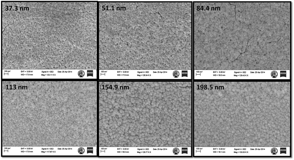
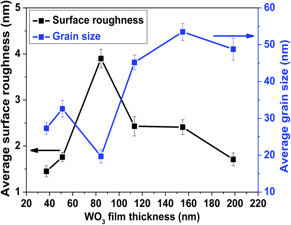
Surface morphologies of the as-deposited films of different thicknesses were studied using FE-SEM (Fig. 1). The topography of the films shows that the films have a porous structure with some black holes or zones on the surface. Films of lesser thickness have some minor cracks on the surface that provide direct conduits for gas molecules to flow inside the film; this may influence the sensor performance.35 The WO3 film of thickness ∼85 nm has a smaller grain size and higher surface roughness, as confirmed by the AFM analysis of the film grain size, as well as the surface roughness data, as shown in Fig. 2.
 |
| | Fig. 1 SEM images of the reactive sputter-deposited WO3 thin films. | |
 |
| | Fig. 2 Variation of average surface roughness and grain size of the WO3 films with different thicknesses. | |
3.2. Electrical characterization of the WO3 films
The graph of the change in the electrical resistance of films with temperature in the range of 25–400 °C is shown in Fig. S4(a).† The resistance of the films, except the 37.3 nm, 113 nm, and 154.9 nm films, decreases rapidly with temperature up to 125 °C and thereafter begins to fall slowly up to 225 °C and afterward again decreases very slowly up to 400 °C. The overall trend of the film resistances indicates the semiconducting nature of the sputter-deposited WO3 films. In fact, two competing processes of thermal excitation of electrons and oxygen adsorption occur simultaneously. In the beginning, the decrease in the film resistance with temperature is because of the thermal excitation of electrons that dominates over the oxygen adsorption process. The slow decrease of film resistance in the temperature range from 125 °C to 225 °C is attributed to adsorption of atmospheric oxygen on the film surface. Herein, oxygen adsorption is not more favourable for the WO3 film; thus, the resistance of films decreases throughout the temperature range. A similar explanation has been reported by other authors.36–38 The inverse absolute temperature of the electrical resistance of the films is shown in Fig. S4(b).† Films exhibit two activation energies in different temperature ranges. The activation energy is calculated using the following relation:| |
R = Ro![[thin space (1/6-em)]](https://www.rsc.org/images/entities/char_2009.gif) exp[(ΔE/kT)] exp[(ΔE/kT)]
| (1) |
where ΔE is the activation energy, Ro is a constant, k is the Boltzmann constant, and T is the absolute temperature. The activation energies thus obtained are listed in Table S1,† which indicates two energies levels – one deep and one shallow near the bottom of the conduction band in the band-gap.
3.3. Nitrogen dioxide (NO2) sensing characteristics of the WO3 films
Room-temperature deposited films were tested several times at each operating temperature to guarantee the reliability of the sensing data. The sensor response (S) of the film is defined as the ratio of change in film resistance upon exposure to test gas to the film resistance in air (at same operating temperatures) and is given by the equationwhere ΔR is change in the resistance of the sensing film before and after exposure to the test gas and R is the initial resistance of film under an air atmosphere. To measure the sensing characteristics of thin films, the sensing setup used is shown in Fig. S5.† The film was mounted in a gas calibration chamber. The gas chamber had the ability to connect to the target gas cylinder along with the synthetic air (80% nitrogen and 20% oxygen) cylinder to set the appropriate concentration of the target gas using mass flow controllers (MFCs). The relative humidity was observed to be ∼45% inside the gas chamber during measurements. The resistance of the WO3 film was found to increase on exposure to NO2 gas due to the oxidizing nature of the gas. The sensing measurements were conducted under dry gas conditions.
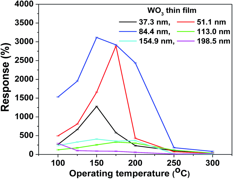
To determine the optimum thickness of the WO3 film for the maximum response to NO2, the gas sensing characteristics of different films towards 0.9 ppm NO2 were measured at different operating temperatures ranging from 100 °C to 300 °C, as shown in Fig. 3. It is well known that a high response depends not only on the optimum film thickness but also on the operating temperature. The present study concluded that the WO3 film thickness of ∼85 nm showed the highest response of ∼3102% to 0.9 ppm NO2 concentration at 150 °C, which was quite a low operating temperature.13
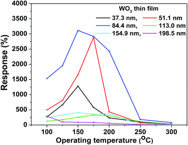 |
| | Fig. 3 Response versus operating temperature plot of the as-deposited WO3 films for a 0.9 ppm NO2 gas concentration. | |
To estimate the stability of the film response towards NO2, the ∼85 nm thick film is exposed multiple times to a 0.9 ppm NO2 concentration to quantify the resistance change of the film on each exposure. The film exhibits degradation in response after each exposure, as indicated by the drift observed in the baseline resistance of the film. The film is able to recover only ∼80% of the resistance, which is changed on exposure to NO2 gas. This may be due to the accumulation of incompletely oxidized gas molecules on the film surface. This results in an incomplete recovery of film resistance upon switching to synthetic air (NO2 exposure is off). To recover the sensor base line drift, the periodic shift to a higher temperature for a short duration is made the part of sensing protocol to desorb the gas molecules from the film surface.2,39 Thus, the temperature impulses of 50 °C and 100 °C of 50 seconds duration are implemented in between the sensing cycle, as shown in Fig. 4. From the initial two response cycles, it is clear that the recovery of film resistance is poor on impulse of 50 °C temperature, as can be seen from the obtained responses, as shown (red dots) in the inset of Fig. 4. This may be due to insufficient thermal energy for the gas molecules to desorb from the film surface. However after a temperature impulse of 100 °C, the base resistance is almost recovered, as shown (green dots) in the inset of Fig. 4. It can be concluded that the film shows a higher drift in sensor response treated with the impulse of 50 °C (red dots) as compared to the response drift in the case of a 100 °C temperature impulse (green dots). This kind of temperature treatment for a short duration is really effective to obtain the reproducible sensor response. In conclusion, temperature pulse of 100 °C is optimum to obtain the reproducible as well as the stable response towards NO2 using the WO3 thin film.
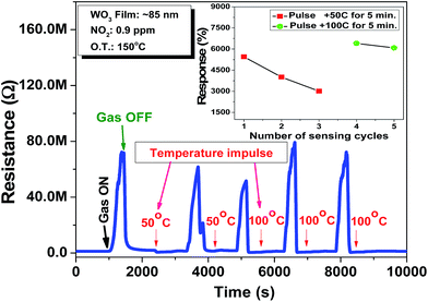 |
| | Fig. 4 Impulse mode of operation of the sensor at an operating temperature of 150 °C for 0.9 ppm NO2 concentration (inset shows the comparison of sensor response with different temperature impulses). | |
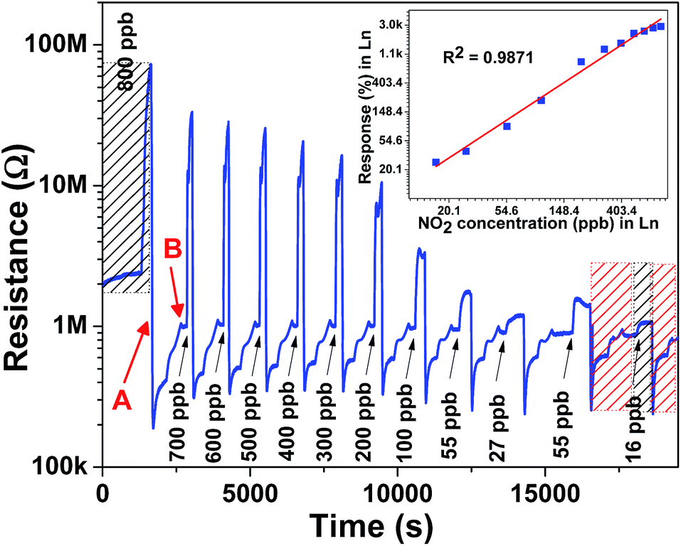
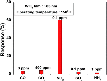
To estimate the low order of detection (LOD), NO2 gas concentration was tested from 16 ppb to 800 ppb at a 150 °C operating temperature with an optimum impulse of 100 °C temperature, as shown in Fig. 5. The film was able to detect 16 ppb [(Rg − Ra)/Ra × 100 = 26%] NO2 concentration, which was comparatively low concentration than that reported in other studies.40,41 Moreover, the WO3 film shows a linear response to different NO2 concentration in the 16–800 ppb range and a detection resolution of 11 ppb for the optimum operating temperature (150 °C) with help of impulsive mode of temperature. Theoretically estimated LOD is 1.6 ppb obtained from the linear fit of response data of film shown in inset of Fig. 5. The comparison of present study along with responses observed by other researchers using different nanostructures of WO3 is shown in Table 1.42–51 The present study on the WO3 thin film-based NO2 sensor concludes that sub-ppb level NO2 detection with high sensitivity and selectivity can be obtained by simple reactive-ion sputtered technique, a scalable process. The WO3 film selectivity towards NO2 was tested in the presence of CO, CO2, SO2, and NH3 gases at 150 °C. The study clearly indicates the high selectivity of the film towards NO2 among other gas species, as represented in Fig. 6.
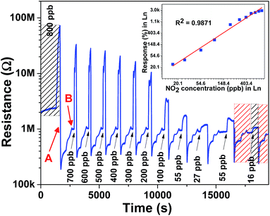 |
| | Fig. 5 Different level NO2 sensing characteristics of the WO3 thin film at 150 °C operating temperature. | |
Table 1 Comparison of NO2 sensing characterisations with different nanostructures of WO3 materials
| Sensing material/morphology |
Synthesis method |
NO2 (ppm) |
Sensor response |
Operating temperature (°C) |
Response time (s) |
Selectivity |
Ref. |
| Flower-like WO3 nanosheets |
Acid treated hydrothermal |
2–80 ppb |
Rg/Ra = 12.8 (2 ppb) |
90 |
— |
Cl2, CO, H2S, NH3, C2H5OH, CH3COCH3 |
21 |
| WO3 powder |
Drop cast method |
0.01–0.25 |
RNO2/Rair × 100% = 1.2 (10 ppb) |
300 |
40 for 100 ppb |
CO, CH3COCH3, H2S, H2, CH4 |
22 |
| Multi-shelled WO3 yolk–shell spheres |
Ultrasonic spray pyrolysis |
50 ppb |
Rg/Ra = 100 (50 ppb) |
100 |
245 for 50 ppb |
CH3COCH3, C2H5OH, CO, NH3, C7H8 |
23 |
| WO3–PEDOT:PSS nanocomposites |
Gravure-printed technique |
50–200 ppb |
Rg/Ra = ∼1.2 (50 ppb) |
RT |
45.1 for 50 ppb |
NH3, H2, CH3COCH3, C2H5OH, CH3OH |
24 |
| Fe-doped WO3 mesoporous |
Facile method |
10–1000 ppb |
Rg/Ra = 1.3 (10 ppb) |
120 |
52 for 10 ppb |
H2, CO2, CH3COCH3, CO, NO2 |
25 |
| Au-doped WO3 microspheres |
Hydrothermal |
1–10 |
Rg/Ra = 1 (1 ppm) |
50 |
75 for 5 ppm |
— |
26 |
| WO3 thin film |
Spray pyrolysis |
1–750 |
(Ra − Rg)/Ra = 0.1 (1 ppm) |
125 |
0.6 for 250 ppm |
— |
42 |
| 3D WO3 nanocolumn bundles |
Hydrothermal |
1–320 |
Rg/Ra = 2.06 (1 ppm) |
110 |
23 for 10 ppm |
— |
43 |
| WO3 hierarchical |
Hydrothermal |
1–20 |
Rg/Ra = 7 (1 ppm) |
100 |
41 for 5 ppm |
— |
44 |
| Au-decorated WO3 nanodomes |
Soft templates |
0.3–5 |
(Rg − Ra)/Ra = 361 (5 ppm) |
250 |
63 for 5 ppm |
CH3COCH3, C2H5OH, NH3, CO, H2, C6H6 |
45 |
| 3-D WO3–rGO hybrid nanostructure |
Hydrothermal |
5–200 |
Rg/Ra = 4.3 (10 ppm) |
90 |
4.1 for 10 ppm |
— |
46 |
| 3DOM WO3/Li |
Colloidal crystal template |
0.5–1 |
Rg/Ra = 55 (0.5 ppm) |
25 |
300 for 0.5 ppm |
C2H5OH, NH3, CH3COCH3, C6H4 (C2H5)2 |
47 |
| Villi-like WO3 nanostructures |
RF sputter |
0.2–5 |
RNO2/REthanol = 500 (5 ppm NO2/50 ppm CH3COCH3) |
250 |
— |
C2H5OH, CH3COCH3, NH3, C7H8, CO |
48 |
| WO3 thin film |
Red-ox route HFCVD |
5–750 |
Rg − Ra/Ra = 32 (5 ppm) |
250 |
— |
— |
49 |
| WO3 nanorods (annealed at 500 °C) |
Glancing angle dc magnetron sputtering |
0.1–2 |
Rg/Ra = ∼27 (2 ppm) |
250 |
— |
— |
50 |
| WO3 nanoparticles |
Sol–gel method |
5–150 |
(Rg − Ra)/Ra × 100% = 16 (5 ppm) |
200 |
24 for 100 ppm |
NH3, H2S, C2H5OH, Cl2, CH3OH |
51 |
| WO3 thin film |
Rf reactive-sputter |
16–3 ppm |
(Rg − Ra)/Ra × 100% = 26 (16 ppb) |
150 |
200 for 16 ppb |
CO, CO2, SO2, NH3 |
Present work |
 |
| | Fig. 6 Selectivity check of the WO3 sensor at the operating temperature of 150 °C. | |
The present investigation of WO3 thickness-dependent NO2 characteristics suggest that a film thickness of ∼85 nm is optimum to achieve a highly sensitive and selective NO2 sensor, which significantly shows the sub-ppb range detection with a quick response and recovery time. Furthermore, to realize the prototype NO2 sensor, we fabricated a sensor device inbuilt on-chip-integrated microheater to control the operating temperature of the WO3 film using MEMS surface micromachining processes, as explained hereinafter. The detailed optimization of the fabrication process of the sensor device is described elsewhere.52
3.4. Fabrication of the NO2 sensor device
A 4′′ wafer was cleaned prior to SiO2 deposition first by piranha solution and then dipped in hydrofluoric acid followed by washing with DI water and drying in nitrogen. The front side SiO2 (1 μm) is used to build the sensor device, and the back side SiO2 (1 μm) is used as a mask for backside Si etching in deep reactive ion etching (DRIE). On top of SiO2, Ti/Pt (10/80 nm) is sputtered to a pattern microheater structure. Then, 200 nm PECVD SiO2 is deposited on top of the microheater (200 μm × 200 μm) to serve as an insulator between the micro-heater and sensing electrodes. Sensing electrodes of sputtered Ti/Pt (10/50 nm) are fabricated on top of the microheater. Later, as optimized, ∼85 nm thick WO3 film is deposited onto the sensing electrodes. Finally, bulk Si from the back side of the microheater is dry etched to form an air cavity to reduce the power consumption of the microheater. The deposition and lift-off process of the WO3 sensing material is conducted using sputtering and photolithography. The schematic of the fabricated sensor device is shown in Fig. 7(a and b). To estimate the WO3 sensing layer thickness, a cross-sectional SEM image of the fabricated sensor chip is shown in Fig. 7(c), which indicates the sensing layer thickness of ∼88 nm on top of the sensor chip stacks. To check the response of the fabricated sensor device towards NO2 gas, the measurement is obtained from the packaged sensor, as shown in Fig. 7(d and e).
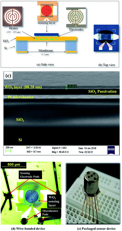 |
| | Fig. 7 (a) Side-view of the micro-sensor, (b) top-view of the micro-sensor, (c) cross-sectional SEM image of the sensor chip, (d) device after wire-bonding, and (e) image of the packaged sensor. | |
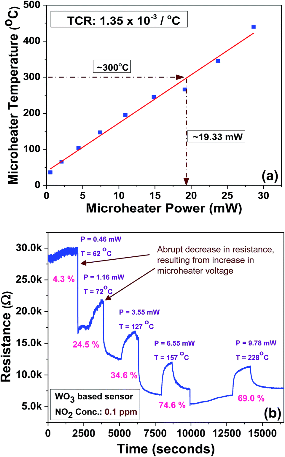
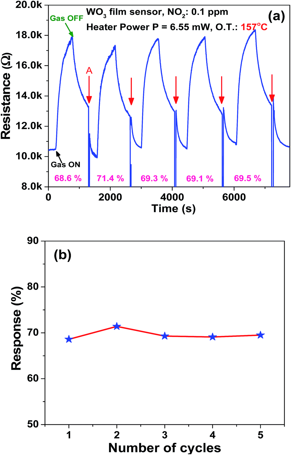
The microheater characterization was conducted to calculate the heater power consumption to achieve different temperatures from the microheater, as shown in Fig. 8(a). The calculated temperature coefficient of resistance (TCR) is 1.35 × 10⁻³ °C−1. Initially, the gas sensitivity is measured under the fixed (0.1 ppm) NO2 concentration at different operating temperatures, ranging from 62 °C to 228 °C, to know the optimum operating temperature to achieve a high response, as shown in Fig. 8(b). The sensor device shows the high response of ∼74.6% at 157 °C, which requires a power of ∼6.55 mW. To examine the repeatability of the fabricated sensor, the sensor is exposed multiple times to a fixed NO2 concentration (0.1 ppm), as shown in Fig. 9(a). The sensor shows an almost repeatable response, but the recovery of the sensor's base resistance is still an issue. Thus, to overcome this issue, the sensor was operated with an impulse mode of temperature by increasing the heater voltage for 20 seconds, which increased the operating temperature by ∼100 °C. As a result, the sensor response is almost repeatable Fig. 9(b). Fabricated sensors are also exposed to different NO2 gas concentrations from 0.1 ppm to 3 ppm under the same operating conditions. For a very low concentration range from 0.1 ppm to 0.5 ppm, the sensor shows a rapid change in response. However, for high concentrations, the increase in response is comparatively slow, as shown in Fig. 10. The rapid change at low concentrations may be because gas-molecules obtain enough thermal energy to react with the sensor surface; this leads to a fast reaction at the sensor sites. On the other hand, with an increase in gas concentration, the gas molecules may be covering the sensor surface very fast; this leads to a slow increase in response. Moreover, the fabricated NO2 sensor shows a nearly linear response in the concentration range from 0.1 ppm to 0.5 ppm with a detection resolution of 100 ppb for the optimum operating conditions, as shown in the inset of Fig. 10. The results indicate that the sensor is capable of detecting a NO2 gas concentration as low as 100 ppb. In fact, many models have been proposed to describe the sensitivity of the semiconducting metal oxide; thus, it can be represented empirically.53 The lowest order of detection of the NO2 sensor is 0.8 ppb, which is calculated by a linear fit of the sensor response data in the concentration range from 0.1 ppm to 0.5 ppm, as shown in the inset of Fig. 10.
 |
| | Fig. 8 (a) Microheater power consumption versus temperature plot. (b) Sensor response at different operating temperatures at a fixed NO2 concentration (0.1 ppm). | |
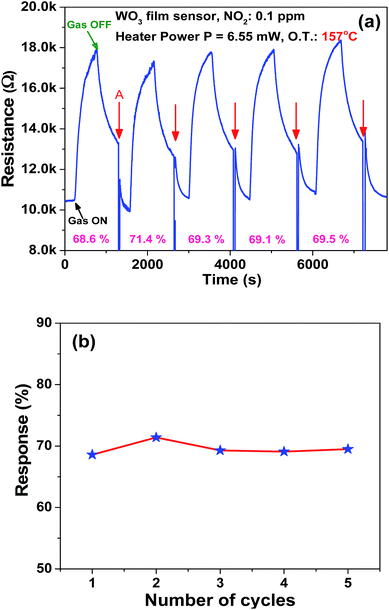 |
| | Fig. 9 (a) Sensor's repeatable response characteristics at a fixed operating temperature of 157 °C and gas concentration of 0.1 ppm (symbol A indicates an abrupt decrease in resistance, resulting from a rapid increase in heater voltage) and (b) sensitivity versus number of cycles curve. | |
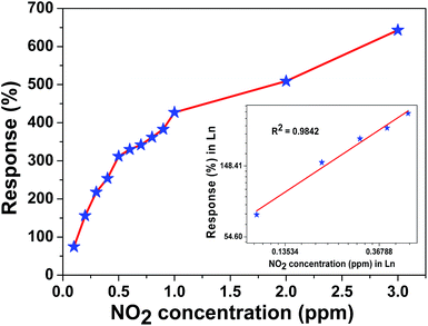 |
| | Fig. 10 Response versus NO2 concentration plot of the fabricated sensor. | |
We have monitored the fabricated NO2 sensor response characteristics to evaluate the sensor reproducibility and stability for a period of more than 6 months to estimate the sensor life. The as-fabricated sensor is found to be very stable during this period. Thus, we propose that the present sensor is a promising candidate for real-time monitoring of NO2 gas in air.
4. Conclusions
In conclusion, film surface morphology plays an important role in deciding the sensing characteristics of thin film-based sensors. XPS analysis of sputter-deposited films shows the desired chemical states. SEM images show that films have a porous microstructure with small cracks, which helps to enhance the sensing reaction because of the deep interaction of gas molecules with the film. The impulse mode of temperature is implemented successfully to produce a highly stable and reproducible sensor response. With these sensors, a detection limit of 16 ppb for NO2 is achieved. This is the lowest detectable concentration with this pristine metal-oxide semiconductor to date. Sensors show high selectivity as well as sensitivity to NO2 gas.
The NO2 sensor device is fabricated successfully using an MEMS platform and tested under different operating conditions to evaluate the performance of the sensor. An impulse mode of temperature is found to be effective to recover the baseline drift in NO2 sensor resistance. The choice of sensor elements on a single diaphragm exhibits fairly good cross-sensitivity, long-term stability, as well as reproducibility towards NO2 gas detection.
Conflicts of interest
There are no conflicts to declare.
Acknowledgements
We thank Meity and DAE for the funding support. We also acknowledge the technical support provided by the National Nano Fabrication Facility (NNFC), Micro and Nano Characterization Facility (MNCF) and Packaging lab at the Centre for Nano Science and Engineering (CeNSE), Indian Institute of Science, Bangalore, India.
Notes and references
- D. Zhang, Z. Liu, C. Li, T. Tang, X. Liu, S. Han, B. Lei and C. Zhou, Detection of NO2 Down to ppb Levels Using Individual and Multiple In2O3 Nanowire Devices, Nano Lett., 2004, 4, 1919–1924 CrossRef CAS.
- L. Shi, Y. Wang, S. Ding, Z. Chu, Y. Yin, D. Jiang, J. Luo and W. Jin, A facile and green strategy for preparing newly-designed 3D graphene/gold film and its application in highly efficient electrochemical mercury assay, Biosens. Bioelectron., 2017, 89, 871–879 CrossRef PubMed.
- L. Shi, Y. Wang, Z. Chu, Y. Yin, D. Jiang, J. Luo, S. Ding and W. Jin, A highly sensitive and reusable electrochemical mercury biosensor based on tunable verticle single-walled carbon nanotubes and a target recycling strategy, J. Mater. Chem. B, 2017, 5, 1073–1080 RSC.
- L. Shi, Z. Chu, Y. Liu, W. Jin and N. Xu, In situ fabrication of three-dimensional graphene films on gold substates with controllable pore structures for high-performance electrochemical sensing, Adv. Funct. Mater., 2014, 24, 7032–7041 CrossRef.
- G. Korotcenkov and B. K. Cho, Engineering approaches for the improvement of conductometric gas sensor parameters Part 1. Improvement of sensor sensitivity and selectivity (short survey), Sens. Actuators, B, 2013, 188, 709–728 CrossRef CAS.
- G. Korotcenkov and B. K. Cho, Engineering approaches for the improvement of conductometric gas sensor parameters Part 2. Decrease of dissipated (consumable) power and improvement stability and reliability, Sens. Actuators, B, 2014, 198, 316–341 CrossRef CAS.
- R. Mariappan, V. Ponnuswamy, P. Surech, N. Ashok, P. Jayamurugan and A. C. Bose, Influence of film thickness on the properties of sprayed ZnO thin films for gas sensor applications, Superlattices Microstruct., 2014, 71, 238–249 CrossRef CAS.
- P. S. Shewale, G. L. Agawane, S. W. Shin, A. V. Moholkar, J. Y. Lee, J. H. Kim and M. D. Uplane, Thickness dependent H2S sensing properties of nanocrystalline ZnO thin films derived by advanced spray pyrolysis, Sens. Actuators, B, 2013, 177, 695–702 CrossRef CAS.
- N. Kakati, S. H. Jee, S. H. Kim, J. Y. Oh and Y. S. Yoon, Thickness dependency of sol–gel derived ZnO thin films on gas sensing behaviors, Thin Solid Films, 2010, 519, 494–498 CrossRef CAS.
- R. R. Salunkhe and C. D. Lokhande, Effect of film thickness on liquefied petroleum gas (LPG) sensing properties of SILAR deposited CdO thin films, Sens. Actuators, B, 2008, 129, 345–351 CrossRef CAS.
- X. Li and G. M. Kale, Influence of thickness of ITO sensing electrode film on sensing performance of planar mixed potential CO sensor, Sens. Actuators, B, 2006, 120, 150–155 CrossRef CAS.
- G. Korotcenkov and B. K. Cho, Thin film SnO2-based gas sensors: Film thickness influence, Sens. Actuators, B, 2009, 142, 321–330 CrossRef CAS.
- A. Hemberg, S. Konstantinidis, P. Viville, F. Renaux, J. P. Dauchot, E. Llobet and R. Snyders, Effect of film thickness of reactively sputtered WO3 submicron thin films used for NO2 detection, Sens. Actuators, B, 2012, 171–172, 18–24 CrossRef CAS.
- I. A. Al-Homoudi, J. S. Thakur, R. Naik, G. W. Auner and G. Newaz, Anatase TiO2 films based CO gas sensor: Film thickness, substrate and temperature effect, Appl. Surf. Sci., 2007, 253, 8607–8614 CrossRef CAS.
- Y.-G. Choi, G. Sakai, K. Shimanoe and N. Yamazoe, Wet process based fabrication of WO3 thin film for NO2 detection, Sens. Actuators, B, 2004, 101, 107–111 CrossRef CAS.
- K. Shimanoe, A. Nishiyama, M. Yuasa, T. Kida and N. Yamazoe, Microstructure control of WO3 film by adding nano-particles of SnO2 for NO2 detection in ppb level, Procedia Chem., 2009, 1, 212–215 CrossRef CAS.
- A. Boudiba, C. Zhang, C. Bittencourt, P. Umek, M.-G. Olivier, R. Snyders and M. Debliquy, Hydrothermal synthesis of two dimensional WO3 nanostructures for NO2 detection in ppb-level, Procedia Chem., 2012, 47, 228–231 CAS.
- T. Kida, A. Nishiyama, M. Yuasa, K. Shimanoe and N. Yamazoe, Highly sensitive NO2 sensors using lamellar-structured WO3 particles prepared by an acidification method, Sens. Actuators, B, 2009, 135, 568–578 CrossRef CAS.
- J. Tamaki, T. Hashishin, Y. Uno, D. V. Dao and S. S ugiyama, Ultrahigh-sensitive WO3 nanosensor with interdigitated Au nano-electrode for NO2 detection, Sens. Actuators, B, 2008, 132, 234–238 CrossRef CAS.
- L. You, X. He, D. Wang, P. Sun, Y. F. Sun, X. S. Liang, Y. Du and G. Y. Lu, Ultrasensitive and low operating temperature NO2 gas sensor using nanosheets assembled hierarchical WO3 hollow microspheres, Sens. Actuators, B, 2012, 173, 426–432 CrossRef CAS.
- C. Wang, R. Sun, X. Li, Y. Sun, P. Sun, F. Liu and G. Lu, Hierarchical flower-like WO3 nanostructures and their gas sensing properties, Sens. Actuators, B, 2014, 204, 224–230 CrossRef CAS.
- B. U. Wojcik, T. A. Vincent, M. F. Chowdhury and J. W. Gardner, Ultrasensitive WO3 gas sensors for NO2 detection in air and low oxygen environment, Sens. Actuators, B, 2017, 239, 1051–1059 CrossRef.
- J.-S. Kim, J.-W. Yoon, Y. J. Hong, Y. C. Kanga, F. A. Hady, A. A. Wazzan and J.-H. Lee, Highly sensitive and selective detection of ppb-level NO2 using multi-shelled WO3 yolk–shell spheres, Sens. Actuators, B, 2016, 229, 561–569 CrossRef.
- Y. Lin, L. Huang, L. Chen, J. Zhang, L. Shen, Q. Chen and W. Shi, Fully gravure-printed NO2 gas sensor on a polyimide foil using WO3–PEDOT:PSS nanocomposites and Ag electrodes, Sens. Actuators, B, 2015, 216, 176–183 CrossRef CAS.
- Z. Zhang, M. haq, Z. Wen, Z. Ye and L. Zhu, Ultrasensitive ppb-level NO2 gas sensor based on WO3 hollow nanospheres doped with Fe, Appl. Surf. Sci., 2018, 434, 891–897 CrossRef CAS.
- Y. Shen, H. Bi, T. Li, X. Zhong, X. Chen, A. Fan and D. Wei, Low-temperature and highly enhanced NO2 sensing performance of Au-functionalized WO3 microspheres with a hierarchical nanostructure, Appl. Surf. Sci., 2018, 434, 922–931 CrossRef CAS.
- Z. Liu, T. Yamazaki, Y. Shen, T. Kikuta and N. Nakatani, Influence of annealing on microstructure and NO2-sensing properties of sputtered WO3 thin films, Sens. Actuators, B, 2007, 128, 173–178 CrossRef CAS.
- A. Sharmaa, M. Tomar and V. Guptaa, WO3 nanoclusters–SnO2 film gas sensor heterostructure with enhanced response for NO2, Sens. Actuators, B, 2013, 176, 675–684 CrossRef.
- C. Cantalini, H. T. Sum, M. Faccio, M. Pelino, S. Santucci, L. Lozzi and M. Passacantando, NO2 sensitivity of WO3 thin film obtained by high vacuum thermal evaporation, Sens. Actuators, B, 1996, 31, 81–87 CrossRef CAS.
- J. Zeng, M. Hu, W. Wang, H. Chen and Y. g. Qin, NO2-sensing properties of porous WO3 gas sensor based on anodized sputtered tungsten thin film, Sens. Actuators, B, 2012, 161, 447–452 CrossRef CAS.
- C. Zhang, A. Boudiba, C. Navio, M.-G. Olivier, R. Snyders and M. Debliquy, Improvement in selectivity of NO2 sensors based on WO3 thin films with MnO2 filters
deposited by radio frequency sputtering, Transducers'11, Beijing, China, 5–9 June 2011 Search PubMed.
- J. N. Yao, P. Chen and A. Fujishima, Electrochromic behavior of electrodeposited tungsten oxide thin films, J. Electroanal. Chem., 1996, 406, 223–226 CrossRef.
- R. Sivakumar, R. Gopalakrishnan, M. Jayachandran and C. Sanjeeviraja, Investigation of X-ray photoelectron spectroscopy (XPS), cyclic voltammetric analyses of WO3 films and their electrochromic response in FTO/WO3/electrolyte/FTO cells, Smart Mater. Struct., 2006, 15, 877–888 CrossRef CAS.
- C. Cantalini, W. Wlodarski, Y. Li, M. Passacantando, S. Santucci, E. Comini, G. Faglia and G. Sberveglieri, Investigation on the O3 sensitivity properties of WO3 thin films prepared by sol–gel, thermal evaporation and r.f. sputtering techniques, Sens. Actuators, B, 2000, 64, 182–188 CrossRef CAS.
- M. Kang, M. Chu, S. W. Kim and J.-W. Ryu, Optical and electrical properties of V2O5 nanorod films grown using an electron beam, Thin Solid Films, 2013, 547, 198–201 CrossRef CAS.
- C. H. Kwon, H.-K. Hong, D. H. Yun, K. Lee, S.-T. Kim, Y.-H. Roh and B.-H. Lee, Thick-film zinc-oxide gas sensor for the control of lean air-to-fuel ratio in domestic combustion systems, Sens. Actuators, B, 1995, 24–25, 610–613 CrossRef.
- P. P. Sahay and R. K. Nath, Al-doped ZnO thin films as methanol sensors, Sens. Actuators, B, 2008, 134, 654–659 CrossRef CAS.
- C. S. Prajapati and P. P. Sahay, Effect of precursors on structure, optical and electrical properties of chemically deposited nanocrystalline ZnO thin films, Appl. Surf. Sci., 2012, 258, 2823–2828 CrossRef CAS.
- D. Morris and R. G. Egdell, Application of V-doped TiO2 as a sensor for detection of SO2, J. Mater. Chem., 2001, 11, 3207–3210 RSC.
- C. Liewhiran, N. Tamaekong, A. Wisitsora-at and S. Phanichphant, The monitoring of H2S and SO2 noxious gases from industrial environment with sensors based on flame-spray-made SnO2 Nanoparticles, Eng. J., 2012, 16, 123–134 CrossRef.
- S. Das, S. Chakraborty, O. Parkash, D. Kumar, S. Bandyopadhyay, S. K. Samudrala, A. Sen and H. S. Maiti, Vanadium doped tin oxide as a novel sulfur dioxide sensor, Talanta, 2008, 75, 385–389 CrossRef CAS PubMed.
- R. Godbole, V. P. Godbole, P. S. Alegaonkar and S. Bhagwat, Effect of film thickness on gas sensing properties of sprayed WO3 thin films, New J. Chem., 2017, 41, 11807–11816 RSC.
- J. J. Qi, S. Gao, K. Chen, J. Yang, H. W. Zhao, L. Guo and S. H. Yang, Vertically aligned, double-sided, and self supported 3D WO3 nanocolumn bundles for low temperature gas sensing, J. Mater. Chem. A, 2015, 3, 18019–18026 CAS.
- Y. Shen, W. Wang, X. Chen, B. Zhang, D. Wei, S. Gao and B. Cui, Nitrogen dioxide sensing using tungsten oxide microspheres with hierarchical nanorod-assembled architectures by a complexing surfactant-mediated hydrothermal route, J. Mater. Chem. A, 2016, 4, 1345–1352 CAS.
- Y. S. Shim, H. G. Moon, D. H. Kim, L. Zhang, S.-J. Yoon, Y. S. Yoon, C.-Y. Kang and H. W. Jang, Au-decorated WO3 cross-linked nanodomes for ultrahigh sensitive and selective sensing of NO2 and C2H5OH, RSC Adv., 2013, 3, 10452–10459 RSC.
- Q. Hao, T. Liu, J. Liu, Q. Liu, X. Jing, H. Zhang, G. Huang and J. Wang, Controllable synthesis and enhanced gas sensing properties of a single-crystalline WO3–rGO porous nanocomposite, RSC Adv., 2017, 7, 14192–14199 RSC.
- Z. Wang, X. Fan, D. Han and F. Gu, Structural and electronic engineering of 3DOM WO3 by alkali metal doping for improved NO2 sensing performance, Nanoscale, 2016, 8, 10622–10631 RSC.
- H. G. Moon, S. D. Han, M.-G. Kang, W.-S. Jung, B. Kwon, C. Kim, T. Lee, S. Lee, S.-H. Baek, J.-S. Kim, H.-H. Park and C.-Y. Kang, Glancing angle deposited WO3 nanostructures for enhanced sensitivity and selectivity to NO2 in gas mixture, Sens. Actuators, B, 2016, 229, 92–99 CrossRef CAS.
- R. Godbole, A. Vedpathak, V. Godbole and S. Bhagwat, Tungsten oxide thin films: detection and trapping of hazardous gases, Mater. Res. Express, 2017, 4, 1–7 Search PubMed.
- M. Horprathum, K. Limwichean, A. Wisitsoraat, P. Eiamchai, K. Aiempanakit, P. Limnonthakul, N. Nuntawong, V. Pattantsetakul, A. Tuantranont and P. Chindaudom, NO2-sensing properties of WO3 nanorods prepared by glancing angle DC magnetron sputtering, Sens. Actuators, B, 2013, 176, 685–691 CrossRef CAS.
- A. T. Mane, S. B. Kulkarni, S. T. Navale, A. A. Ghanwat, N. M. Shinde, J.-H. Kim and V. B. Patila, NO2 sensing properties of nanostructured tungsten oxide thin films, Ceram. Int., 2014, 40, 16495–16502 CrossRef CAS.
- C. S. Prajapati, R. Soman, S. B. Rudraswamy, M. M. Nayak and N. Bhat, Single chip gas sensor array for air quality monitoring, J. Microelectromech. Syst., 2017, 26, 433–439 CrossRef.
- C. S. Prajapati, D. Visser and S. Anand, Navakanta Bhat, Honeycomb type ZnO nanostructures for sensitive and selective CO detection, Sens. Actuators, B, 2017, 252, 764–772 CrossRef CAS.
Footnote |
| † Electronic supplementary information (ESI) available. See DOI: 10.1039/c7ra13659e |
|
| This journal is © The Royal Society of Chemistry 2018 |
Click here to see how this site uses Cookies. View our privacy policy here. 
 Open Access Article
 This Open Access Article is licensed under a
  * and
Navakanta Bhat
* and
Navakanta Bhat