
 Open Access Article
 This Open Access Article is licensed under a
 Creative Commons Attribution 3.0 Unported Licence
Highly enhanced response of MoS2/porous silicon nanowire heterojunctions to NO2 at room temperature†
Shufen Zhao a,
Zhengcao Li*ab,
Guojing Wanga,
Jiecui Liaoa,
Shasha Lva and
Zhenan Zhuc
a,
Zhengcao Li*ab,
Guojing Wanga,
Jiecui Liaoa,
Shasha Lva and
Zhenan Zhuc
aState Key Laboratory of New Ceramics and Fine Processing, School of Materials Science and Engineering, Tsinghua University, Beijing 100084, China. E-mail: zcli@mail.tsinghua.edu.cn
bKey Laboratory of Advanced Materials (MOE), School of Materials Science and Engineering, Tsinghua University, Beijing 100084, China
cDepartment of Engineering Physics, Tsinghua University, Beijing 100084, China
First published on 21st March 2018
Abstract
Molybdenum disulfide/porous silicon nanowire (MoS2/PSiNW) heterojunctions with different thicknesses as highly-responsive NO2 gas sensors were obtained in the present study. Porous silicon nanowires were fabricated using metal-assisted chemical etching, and seeded with different thicknesses. After that, MoS2 nanosheets were synthesized by sulfurization of direct-current (DC)-magnetic-sputtering Mo films on PSiNWs. Compared with the as-prepared PSiNWs and MoS2, the MoS2/PSiNW heterojunctions exhibited superior gas sensing properties with a low detection concentration of 1 ppm and a high response enhancement factor of ∼2.3 at room temperature. The enhancement of the gas sensitivity was attributed to the layered nanostructure, which induces more active sites for the absorption of NO2, and modulation of the depletion layer width at the interface. Further, the effects of the deposition temperature in the chemical vapor deposition (CVD) process on the gas sensing properties were also discussed, and might be connected to the nucleation and growth of MoS2 nanosheets. Our results indicate that MoS2/PSiNW heterojunctions might be a good candidate for constructing high-performance NO2 sensors for various applications.
1. Introduction
Gas sensors play an important role in monitoring the environment and detecting air pollution. Many factors affect the gas sensing capacity of a gas sensor, including the materials, sensing mechanism and environmental effects (temperature, humidity).1,2 Recently, many researchers have devoted their efforts to developing sensors with high sensitivity and low operating temperatures.3 It is well known that semiconducting materials are used in gas sensors, such as metal oxides, silicon, and two-dimensional (2D) materials. Metal oxides are a common material to be employed for gas detection.4–6 However, they exhibit poor conductivity and require high temperatures to operate.7 In particular, silicon and two-dimensional (2D) materials have been widely used in low-temperature sensors.8,9Silicon has many advantages including stability, abundance and optical properties, and it can be employed in microelectronic technologies.10 Among these silicon-based materials, PSiNW materials are one of the most promising n-type semiconductors, as they possess large surface areas and high chemical reactivity.11 For these reasons, they are widely used in gas sensing devices. PSiNWs are impressive as they can be easily integrated with other semiconductors to lower the operating temperature of the resulting gas sensor.12 However, there are several disadvantages, such as poor sensitivity and oxidation of the surface of the material at room temperature.
2D materials such as graphene and MoS2 are developing rapidly, with high surface-to-volume ratios.13 MoS2 has a 2D layered structure and its band gap is affected by the number of stacked layers.14 Monolayer MoS2 is an n-type semiconductor with a direct band gap of ∼1.9 eV, while bilayer and thicker MoS2 crystals have indirect band gaps of ∼1.3 eV.15,16 MoS2 is used as a gas sensor mainly because of its various sites (sulfur defects, vacancies, and edge sites).17 Thermal treatments can improve device performance.18 Moreover, compared with other synthetic methods, CVD has the obvious advantages of thickness control19,20 and the ability for large-scale growth of MoS2.21
MoS2 could act as a protecting layer for PSiNWs against oxidation damage when applied to gas sensor devices. However, few studies have reported application of MoS2/PSiNW heterojunctions to gas sensing. In this paper, MoS2/PSiNW heterojunctions fabricated on a substrate with Ag electrodes are presented. The effects of the thickness and deposition temperatures on the gas sensing properties were also explored. As a consequence, MoS2/PSiNW heterojunctions with different morphologies showed high sensitivity, low operating temperatures and fast response/recovery properties. This study represents an important step to improve gas sensing properties through the synthesis of MoS2/PSiNW heterojunctions.
2. Experimental section
2.1. Sensor fabrication process
MoS2/PSiNW heterojunctions were fabricated on 〈100〉 orientation, n-type Si substrates using Ag-assisted chemical etching, direct current (DC) magnetic sputtering and chemical vapor deposition (CVD) methods, as shown in Fig. 1. The fabrication process is further explained as follows. The silicon wafers were cut and ultrasonically cleaned in acetone, ethanol and deionized water for 15 min each. Then they were immersed in boiling H2SO4/H2O2 solution at 135 °C for 1 h to remove the organic contaminants. To remove the silicon oxide layer, they were treated with 5% HF before use. PSiNWs were synthesized using a metal-assisted chemical etching method. Pre-treated silicon wafers were placed into a mixed solution of 4.8 M HF and 5 mM AgNO3 to obtain a layer of Ag nanoparticles, and were then immersed into a solution of 4.8 M HF and 0.3 M H2O2 at 30 °C. Ag nanoparticles on the silicon substrate play an important role as catalysts in the etching process. An etching time of 15 min was selected, and we obtained PSiNWs after the etching process was finished. To remove residual Ag nanoparticles and the silicon oxide layer, the PSiNWs were dipped in HNO3 solution and HF solution successively. After each procedure, they were washed with plenty of water.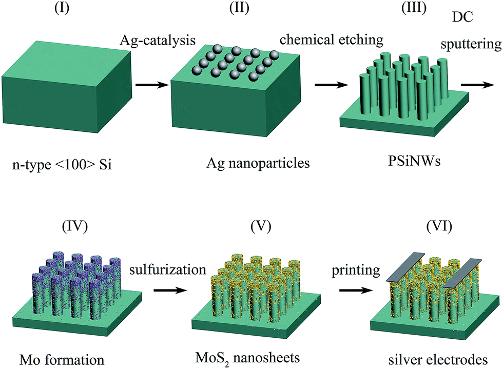 | ||
| Fig. 1 Fabrication process of the MoS2/PSiNW-based sensor devices. | ||
Mo atoms were deposited onto the PSiNW substrate using direct current (DC) magnetic sputtering, which could control different thicknesses. The deposition was carried out with 70 W power and a working Ar pressure of 0.3 Pa, and the base pressure was below 10−4 Pa. We selected three parameters of the magnetic sputtering time for the Mo seed layers (1 min, 3 min and 5 min), used to control the thickness of the Mo seed layer on the PSiNW substrate.
MoS2 nanosheets were grown on PSiNWs using chemical vapor deposition (CVD). After the deposition of seed layers on the PSiNW substrates, the substrates were placed at the center of the furnace and sulfur powder (1.5 g) was placed at the upstream end. Two temperature ranges were used to separate the PSiNW substrates covered by Mo seed layers and sulfur powder. Sulfur powder (1.5 g) was placed upstream of the quartz tube at a distance of 10 cm from annealing furnace. At the beginning, a PSiNW substrate covered by Mo seed layers was put on a quartz boat, which was still downstream of quartz and outside of the annealing furnace. The annealing furnace needed to be checked for air tightness and N2 was injected to get rid of residual air. The temperature of the center zone was increased to 770 °C at a ramp rate of 14 °C for the growth process and the upstream zone was heated to 130 °C at a ramp rate of 26 °C for vaporization of elemental sulfur powders. After the center zone had risen to 770 °C and the upstream zone had been maintained at 130 °C, the quartz boat was pushed into the center of the furnace with a magnet and maintained for 90 min. Finally, the samples were moved out of the furnace after natural cooling. During whole process, the flow rate of Ar carrier gas was maintained at 200 standard cubic centimeters per minute (SCCM). We marked samples as “MoS2/PSiNWs-1 min”, “MoS2/PSiNWs-3 min” and “MoS2/PSiNWs-5 min”, according to the magnetic sputtering time (1 min, 3 min and 5 min, respectively) of the Mo seed layers. To study the effect of deposition temperature in the chemical vapor deposition process on the gas sensing behaviors, three distinct MoS2/PSiNW heterojunctions with different deposition temperatures of 720 °C, 770 °C and 820 °C were synthesized, named “S-1”, “S-2” and “S-3”, respectively.
2.2. Characterization
The surface morphologies and microstructures were characterized using scanning electron microscopy (SEM, JEOL-JSM 7001F, Tokyo, Japan) and high-resolution transmission electron microscopy (HRTEM, JEM-2100F). X-ray photoelectron spectroscopy (XPS, ESCALAB250Xi, Thermo, Waltham, MA, America) used the C 1s signal (284.8 eV) as a reference to calibrate the binding energy. X-ray diffraction (XRD) patterns were obtained on a Rigaku Smart Lab (Tokyo, Japan) and Raman spectra were obtained using a Lab Ram HR Evolution Micro Raman Spectrometer. These patterns and spectra were used to analyze the structural features and phase purity of the MoS2/PSiNW heterojunctions. Raman microscopy was performed with an excitation wavelength of 532 nm.2.3. Gas sensing measurements
To measure the gas sensing properties of the samples, two silver electrodes were deposited onto them using printing, and connected to a digital resistance measurement system. Then the experiment was carried out in a home-made system. The testing chamber used was a 250 mL metal chamber, and gas would fill the chamber in 30 seconds based on the flow rate used. Gases used for the test were NO2 (0.01% NO2 with 99.99% N2) and pure N2 (99.999%). At the beginning, pure N2 was needed to inject into the chamber. After the resistance of the samples reached a stable value, gases were mixed to obtain certain concentrations and injected into the chamber until a new constant value of the concentration was achieved. The measuring system recorded the resistance of the sensors at all times. By controlling the mass flow to change the specific gas concentration, the computer recorded the resistance change of the samples versus the concentration of NO2. The gas filled the chamber within few seconds and such a setup was found to be appropriate for the gas sensing measurements. Response was one of main gas sensing properties, which is defined as follows:where Rg is the measured electric resistance of a gas sensor at a certain concentration of NO2 and R0 is the resistance in a pure N2 atmosphere.

3. Results and discussion
Scanning electron microscopy (SEM) was used to characterize the morphology of the samples. Fig. 2a and c show the top view and side view of the PSiNWs obtained via Ag-assisted chemical etching. The surface morphology of the PSiNWs is rough and the tip parts are clustered. The obtained porous silicon nanowires are arranged vertically on the silicon substrates with good alignment. MoS2 nanosheets grown on wafers using CVD are shown in Fig. 2b and d. The MoS2 nanosheets are distributed on the silicon substrate uniformly. The observable MoS2 film consists of vertically standing nanosheets. Abundant MoS2 nanosheet layers provide large quantities of edge sites, which are beneficial for gas sensing properties.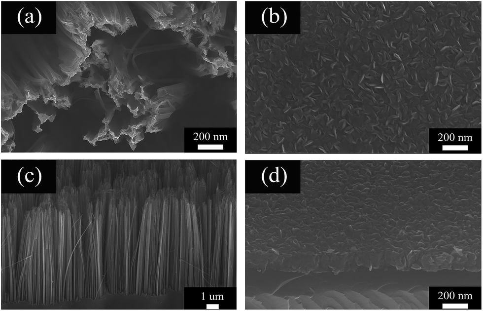 | ||
| Fig. 2 SEM images of PSiNWs: (a) top view (c) side view. SEM images of MoS2 nanosheets on wafers: (b) top view (d) side view. | ||
Fig. 3 shows the thickness evolution and surface morphology of MoS2 nanosheets grown on PSiNWs using CVD. The deposition rate of MoS2 on the silicon wafers was ∼20 nm min−1. Fig. 3a and c show the top view and side view of edge-exposed MoS2 nanosheets on PSiNWs. The MoS2 nanosheets are grown densely on the top and lateral surfaces of the PSiNWs, which increases the reactive areas for gas molecules. The magnified view of the surface with obvious edges indicates the possibility of layer structure growth. An increase in the thicknesses of the MoS2 nanosheets seems to appear near the edges, where they begin to cluster (Fig. 3b and d). Fig. 3c and d show that isolated nanosheets are clustered together to form densely layered stacked structures. One can see that quantities of MoS2 nanosheets are interconnected with each other and generate many holes or channels for gas to quickly diffuse from the surface to the inside of the nanostructure. The distribution of MoS2 nanosheets on the lateral surface of PSiNWs was further examined using transmission electron microscopy (TEM).
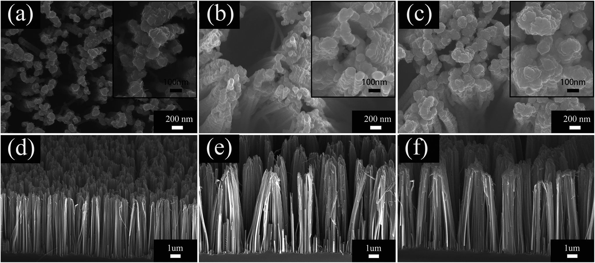 | ||
| Fig. 3 SEM images of top views of (a) MoS2/PSiNWs-1 min, (b) MoS2/PSiNWs-3 min and (c) MoS2/PSiNWs-5 min and side views of (d) MoS2/PSiNWs-1 min, (e) MoS2/PSiNWs-3 min and (f) MoS2/PSiNWs-5 min. Illustrations in (a–c) are high resolution SEM of top view. | ||
TEM was used to analyze the nanostructure and elemental distribution. Fig. 4a shows that the rod-like morphology still remains after forming MoS2 nanosheets on the PSiNW nanostructures. The MoS2 nanosheets are uniformly distributed on the surface of a single porous silicon nanowire. Fig. 4b clearly shows that each layer consists of an edge atomic structure with the S–Mo–S sequence, because the Mo atoms are heavier and appear brighter. The thickness of the Mo seed layer can change the horizontal and vertical alignment of MoS2.22 Many stripes are at the edges of MoS2 nanosheets, which reveal vertically aligned 2D MoS2 layers. Some grains are composed of a large number of self-assembled MoS2 layers with an interlayer spacing of 0.625 nm, which is consistent with the theoretical spacing for (002) planes of the hexagonal MoS2 nanostructures. A selective area electron diffraction (SAED) pattern (Fig. 4b inset) reveals that the MoS2/PSiNWs have a polycrystalline structure. The elemental distributions of Si, Mo and S are summarized in Fig. 4d. The summarized curve shows only the distribution of Mo and Si atoms, because distribution curves of Mo and S are coincident, which can be confirmed in Fig. 4 (1) and (2). Where a Mo atom is present, S atom will react with it to form MoS2. Si atoms are mainly distributed inside of the MoS2/PSiNW nanostructures, while Mo and S are distributed on the edges and surfaces.
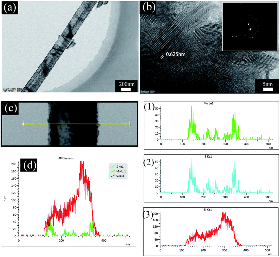 | ||
| Fig. 4 (a) The morphology of MoS2/PSiNW nanostructures. (b) The high-resolution TEM image and selective area electron diffraction (SAED) pattern. (c) The site of line scanning and (d) the elemental distribution of Si, Mo and S. Details for the elements Mo (1), S (2) and Si (3). | ||
The structural details and phase purity of MoS2/PSiNW crystals were studied using XRD. All of the synthesized samples were measured with diffraction peaks in the range of 5–60°, as shown in Fig. 5a. The diffraction peaks of the MoS2 nanosheets are observed at 14.42° and 40°, which correspond to the (002) and (103) planes (JCPDS no. 37-1492). A strong peak at 33° that belongs to Si (200) was observed.
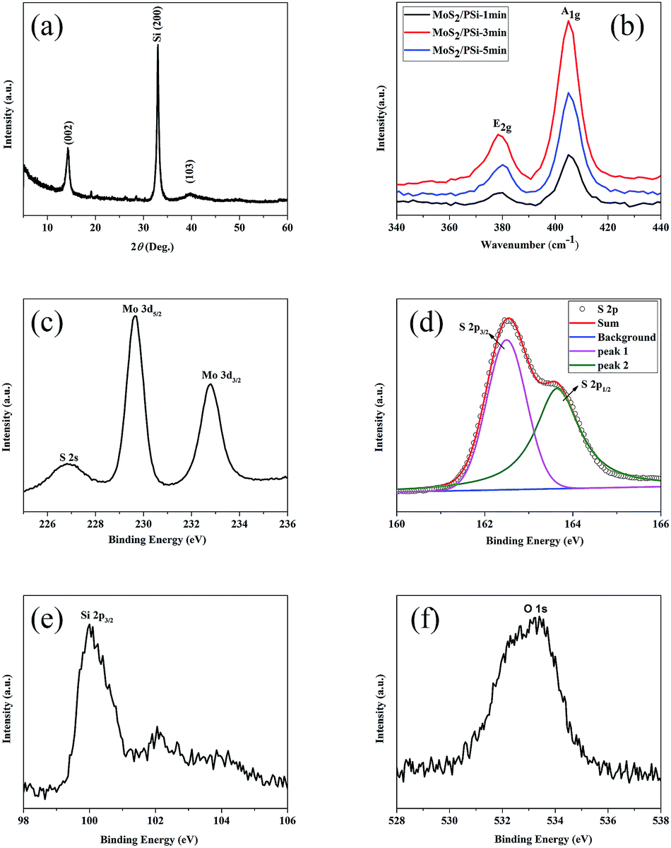 | ||
| Fig. 5 (a) X-ray diffraction (XRD) pattern of MoS2 nanosheets grown on PSiNWs. (b) Raman spectra of MoS2 on PSiNWs with two major peaks: E2g and A1g vibration modes. XPS spectra of (c) Mo 3d, (d) S 2p, (e) Si 2p and (f) O 1s in MoS2/PSiNW samples. | ||
Raman spectra give many properties of the material, namely, structural features, orientation of the facets in the crystal, transition of the material, bonding details, thermal conductivity and compositional detail.23 As Fig. 5b shows, MoS2 has two major peaks: E2g and A1g vibrational modes of the Mo–S bonds near 380 cm−1 and 405 cm−1. E2g represents the in-plane vibrational mode of the Mo and S atoms and A1g represents the out-of-plane vibrational mode of S atoms.24 The peak position difference (n) between E2g and A1g is about 25 cm−1, which is consistent with those observed for bulk MoS2.25 The result is quite sensitive to the thickness of 2-D layered material systems, and that is consistent with what has been reported.26,27 Another feature observed in the Raman spectra is the intensity ratio of E2g/A1g, the value of which is approximately 0.6. The value indicates an obvious out-of-plane vibration (A1g) mode over in-plane vibration (E2g), reflecting the dominantly exposed MoS2 edge sites. The result proves it is typical vertical growth,28,29 which is consistent with the TEM result shown in Fig. 4b.
The surface composition and chemical states of the MoS2/PSiNW nanostructure were measured using X-ray photoelectron spectroscopy (XPS).28 Fig. 5c exhibits the Mo 3d spectrum of the MoS2/PSiNW nanostructure. Two peaks at 229.65 and 232.75 eV are attributed to Mo 3d5/2 and Mo 3d3/2 of Mo4+.30 The other peak at 226.85 eV is in agreement with S2− 2s.31 The S 2p spectrum in Fig. 5d shows two double peaks at 162.5 and 163.7 eV, which are ascribed to S 2p3/2 and S 2p1/2 of S2−, respectively.32 The binding energy is also consistent with previous reports (2p3/2: 162.4 eV and 2p1/2: 163.3–164.14 eV).33–35 Fig. 5e shows that Si has two valence states. The binding energy of Si (2p3/2) observed at 99.95 eV indicates the existence of Si–Si. Fig. 5f shows the O 1s spectrum, indicating a peak at 533.05 eV corresponding to silicon oxide.
4. Gas studies
4.1. Gas-sensing properties
Fig. 6 shows the response and recovery curves of the MoS2/PSiNW heterojunctions with different thicknesses and substrates at room temperature. The sensitivity was measured upon sequential NO2 exposures in the range of 1–50 ppm. The time-dependent gas sensing behaviors toward different concentrations of NO2 are shown in Fig. 6a. MoS2/PSiNWs-3 min exhibited the most sensitivity to NO2, in comparison to MoS2/PSiNWs-1 min and MoS2/PSiNWs-5 min. The highest limit of detection was at 1 ppm. The recovery (60 min after exposure to NO2) could not be fully completed in cycles of 50–1 ppm. The phenomenon was also observed in a graphene-based sensor36 and in previous sensor reports.37 Fig. 6b shows the sensing response as a function of gas concentration. The highest response values (MoS2/PSiNWs-3 min) of each cycle were 0.27, 5.72, 10.55, 17.8 and 28.4% with NO2 concentrations of 1, 5, 10, 20, 50 ppm. This study revealed the influence of the thickness of MoS2 on the gas sensing properties of MoS2/PSiNW heterojunctions. The different thicknesses of the MoS2 nanosheets on PSiNWs could change the energy levels of the conduction and valence bands, which has been shown in an earlier report.38 Fig. 6c shows the dynamic response with different substrates, such as MoS2/PSiNWs, MoS2, and PSiNWs sensors. Among three sensors, MoS2/PSiNWs showed the highest response to NO2. Its response was nearly linear and increased by a factor of 2.3 in comparison to that of PSiNWs as shown in Fig. 6d. The formation of MoS2/PSiNW heterojunctions has improved the gas sensing properties greatly.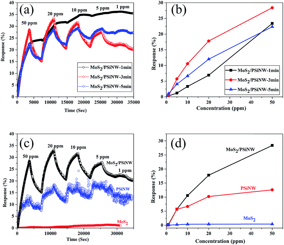 | ||
| Fig. 6 NO2 gas-sensing properties of MoS2/PSiNW nanostructures with different thicknesses of MoS2 nanosheets: (a) time-dependent gas-sensing behaviors toward different concentrations of NO2; (b) the response as a function of gas concentration. The study of gas properties with different substrates: (c) dynamic response in different NO2 concentrations; (d) response values of NO2 concentrations. | ||
Fig. 7a shows time-dependent gas-sensing behavior toward different concentrations of NO2. Compared with S-1 and S-3, S-2 exhibited a higher sensitivity to NO2. Moreover, S-1 and S-3 had no recovery at any cycle, while S-2 showed good recovery. The response value was further studied, and the results are shown in Fig. 7b. Compared with S-1 (6% to 50 ppm) and S-3 (7.7% to 50 ppm), S-2 (28.4% to 50 ppm) exhibited the highest response to NO2 and increased by a factor of 4. This phenomenon is attributed to the decreased defects and grain boundaries. With increasing temperature from 720 °C to 820 °C, the chemical reaction was accelerated and the adsorption and diffusion of sulfur molecules at the interface were strengthened, which increased crystallite size and decreased the grain boundaries (see ESI†). Moreover, the number of defects would be decreased. The crystallite size of MoS2 with the deposition temperature of 820 °C was too large, covering the surfaces of the MoS2/PSiNWs and perturbing interfacial gas molecule diffusion considerably at the molecule surface. The device with deposition temperature of 720 °C could not react completely, resulting in unstable structures. This could be explained by the rapid transfer charge in MoS2 and the high accumulation of electrons at the interface after increasing the annealing temperature.39,40 Therefore, the optimum deposition temperature was found to be 770 °C.
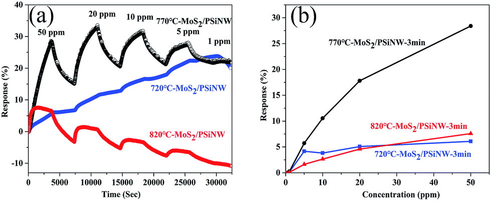 | ||
| Fig. 7 Gas sensing properties to NO2 of S-1, S-2 and S-3: (a) time-dependent gas-sensing behaviors toward different concentrations of NO2; (b) the response as a function of gas concentration. | ||
Fig. 8a shows the current–voltage (I–V) curves of the MoS2/PSiNW heterojunction in dry air and NO2 gas. The measurements were performed 60 min later after the device was put under the above conditions. The I–V curves exhibited good rectification characteristics at room temperature. The rectification ratio (I+/I−) at the voltage of ±5 V for this device was about 2.6.
 | ||
| Fig. 8 (a) I–V curves of MoS2/PSiNW heterojunctions in air and NO2. (b) Equivalent electrical resistance model of MoS2/PSiNW heterojunctions schematic illustration of using CVD to grow MoS2 nanosheets on PSiNWs. (c) Schematic illustration of the energy band of MoS2/PSiNW heterojunction structures. | ||
The MoS2–Ag contacts were ohmic in nature, therefore, the rectifying I–V characteristics were mainly attributed to the MoS2/PSiNW heterojunction. When the air conditions were changed to NO2, obvious changes in the I–V curves of the device were observed. As shown in the figure, the current decreased largely in both the forward and reserve directions. This demonstrates that the electrical properties of the junctions were dependent on NO2. Thus, this MoS2/PSiNW heterojunction device could function as a gas sensor. This is also confirmed in Table 1 by the comparison of the sensitivity to NO2 of other sensors based on different MoS2 nanostructures. The mechanism will be explained in detail later.
| Sensing material | Fabrication method | T (°C) | NO2 (ppm) | Response (%) | Reference |
|---|---|---|---|---|---|
| MoS2/PSiNWs | Chemical etching + CVD | RT | 50 | 28.4% | Present work |
| MoS2 film | CVD | RT | 50 | 17.1% | 41 |
| rGO | Hydrolysis method | RT | 50 | 10.8% | 42 |
| MoS2/carbon nanotube | CVD | RT | 50 | 12.6% | 43 |
| MoS2/TiO2 nanotube | Anodization + hydrothermal method | 150 | 50 | 14.2% | 44 |
| MoS2/Au | Drop-coating | 60 | 50 | 2.2 | 45 |
| rGO/ZnO | Spraying | RT | 50 | 3.05 | 46 |
| rGO/TiO2 | Hydrothermal method | RT | 50 | 15.9 | 47 |
4.2. Gas sensing mechanism
The above-mentioned results reveal that the MoS2/PSiNW heterojunctions exhibited good gas sensing properties to NO2 at room temperature. The high sensitivity is due to the layered nanostructures that induce more active sites for the absorption of NO2 and the modulation of changes to the band bending and depletion layer width at the interface. Moreover, MoS2 has a remarkable concentration of S vacancies (5%).48 When the sensor is exposed to nitrogen dioxide, NO2 molecules act as electron acceptors and form NO2− (ads) through capturing free electrons from the conduction band of the MoS2 sheets. An electron depletion layer will be formed in the process, which leads to an increase in sensor resistance. When nitrogen gas contacts surface of the sensor, N2 molecules will react with nitrogen dioxide ions and release the trapped electrons back to the conduction band, decreasing the electron depletion layer width and increasing the resistance of the sensor. The reaction process can be shown as follows:| MoS2 + NO2 (gas) + e− = MoS2 + NO2− (ads) | (1) |
| 2NO2− (ads) + N2 → 4NO + 2e− | (2) |
The work function and the band gap of n-Si are 4.21 and 1.12 eV, respectively, while the work function and the band gap of MoS2 are 1.3 and 4.33 eV, respectively. The Fermi level of n-Si is higher than that of MoS2 and thus the electrons transfer through the interface from n-Si to MoS2 until their Fermi levels equalize, as shown in Fig. 8c. When the device is exposed to NO2, larger amounts of NO2 molecules are absorbed on the surface of the MoS2 film. Subsequently, some NO2 molecules can be injected into the whole layers of film through the grain boundaries, and even reach the interface area of the junction. NO2 captures free electrons from the conduction band of MoS2 sheets, leading to a reduction in the charge carriers in it,49,50 and increasing the resistance of MoS2. A depletion layer can be formed at the interface of MoS2/PSiNWs. Moreover, the Fermi levels of the MoS2 films shift toward the valence band as has been previously reported,51 and the energy barrier increases at the interface of MoS2/PSiNWs. The sensing mechanism can be explained by the equivalent electrical circuit, as shown in Fig. 8b. The resistance of the MoS2/PSiNW heterojunctions is composed of the resistance of the MoS2 (RMoS2), the barrier (RB) and the PSiNWs (RSi).52 RSi does not show any obvious change after exposure to NO2 due to the heavy doping of Si (0.01–0.05 Ω × cm). RMoS2 and RB mainly determine the resistance variation of the MoS2/PSiNW heterojunction. Fig. 8c shows an obvious potential barrier in the device. The properties of this barrier can greatly affect the resistance of the device as a result of its exponential relationship.53 After adsorption, the charge transfer will lead to a low density of electrons on the MoS2 side in the heterojunction, which increases the barrier of the heterojunction (RB). This is confirmed by the I–V curve in Fig. 8a. It has been reported that the variation of barrier height and width due to gas adsorption can significantly change the resistance.54,55 Therefore, MoS2/PSiNWs exhibit superior gas sensing properties compared to MoS2 and PSiNW sensors (Fig. 6c).
5. Conclusion
We demonstrate a new and simple fabrication method of MoS2/PSiNW heterojunctions. In this approach, PSiNWs were obtained via Ag-assisted chemical etching, and then MoS2 nanosheets were synthesized using sulfurization of direct-current (DC)-magnetic-sputtering Mo films on PSiNWs. The MoS2/PSiNW heterojunctions exhibit superior gas sensing properties with a high response enhancement factor of ∼2.3 at room temperature, in comparison with MoS2 and PSiNWs. The MoS2/PSiNWs-3 min with MoS2 thickness of ∼60 nm showed a maximum response of 28.4% to 50 ppm NO2 and a highest limit of detection at 1 ppm. Additionally, MoS2/PSiNWs fabricated using different deposition temperatures in the chemical vapor deposition (CVD) process were also measured and the results show that the optimum deposition temperature was 770 °C. The enhancement in gas sensing performances is attributed to the predominant geometrical morphology and effect of the depletion layer width at the interface. Moreover, a remarkable concentration of S vacancies in MoS2 acted as independent active sites, magnifying the gas sensing properties of PSiNWs, by improving the interaction of molecules with defects. Therefore, MoS2/PSiNW heterojunctions could stimulate greater innovation for future sensor technologies.Conflicts of interest
There are no conflicts to declare.Acknowledgements
The authors are grateful to the support of the Major National S&T (No. ZX069) and National Natural Science Foundation of China (No. 61176003).References
- Y. Q. Zhang, Z. Li and T. Ling, et al., J. Mater. Chem. A, 2016, 4(22), 8700–8706 CAS.
- X. H. Liu, P. F. Yin and S. A. Kulinich, et al., ACS Appl. Mater. Interfaces, 2017, 9(1), 602 CAS.
- X. Liu, M. Hu and Y. Wang, et al., J. Alloys Compd., 2016, 685, 364–369 CrossRef CAS.
- R. Kumar, O. Al-Dossary and G. Kumar, et al., Nano-Micro Lett., 2015, 7(2), 97–120 CrossRef.
- T. Kida, A. Nishiyama and Z. Hua, et al., Langmuir, 2014, 30(9), 2571–2579 CrossRef CAS PubMed.
- Y. S. Shim, L. Zhang and D. H. Kim, et al., Sens. Actuators, B, 2014, 198(4), 294–301 CrossRef CAS.
- M. A. Worsley, S. J. Shin and M. D. Merrill, et al., ACS Nano, 2015, 9(5), 4698–4705 CrossRef CAS PubMed.
- D. Wu, Z. Lou and Y. Wang, et al., Nanotechnology, 2017, 28(43), 435503 CrossRef PubMed.
- S. Y. Cho, S. J. Kim and Y. Lee, et al., ACS Nano, 2015, 9(9), 9314 CrossRef PubMed.
- S. Lv, Z. Li and C. Chen, et al., ACS Appl. Mater. Interfaces, 2015, 7(24), 13564 CAS.
- J. Liao, Z. Li and G. Wang, et al., Phys. Chem. Chem. Phys., 2016, 18(6), 4835 RSC.
- P. Dwivedi, S. Das and S. Dhanekar, ACS Appl. Mater. Interfaces, 2017, 9(24), 21017–21024 CAS.
- S. W. Fan, A. K. Srivastava and V. P. Dravid, Sens. Actuators, B, 2010, 144(1), 159–163 CrossRef CAS.
- S. Heo, R. Hayakawa and Y. Wakayama, J. Appl. Phys., 2017, 121(2), 024301 CrossRef.
- K. F. Mak, C. Lee and J. Hone, et al., Phys. Rev. Lett., 2010, 105(13), 136805 CrossRef PubMed.
- A. Splendiani, L. Sun and Y. Zhang, et al., Nano Lett., 2010, 10(4), 1271 CrossRef CAS PubMed.
- M. Donarelli, S. Prezioso and F. Perrozzi, et al., Sens. Actuators, B, 2015, 207, 602–613 CrossRef CAS.
- G. Korotcenkov and B. K. Cho, Sens. Actuators, B, 2011, 156(2), 527–538 CrossRef CAS.
- A. Zobel, A. Boson and P. M. Wilson, et al., J. Mater. Chem. C, 2016, 4(47), 11081–11087 RSC.
- C. Nie, L. Yu and X. Wei, et al., Nanotechnology, 2017, 28(27), 275203 CrossRef PubMed.
- W. Zhao, H. Yu and M. Liao, et al., Semicond. Sci. Technol., 2017, 32(2), 025013 CrossRef.
- S. Y. Cho, S. J. Kim and Y. Lee, et al., ACS Nano, 2015, 9(9), 9314–9321 CrossRef PubMed.
- D. J. Late, Y. K. Huang and B. Liu, et al., ACS Nano, 2013, 7(6), 4879–4891 CrossRef CAS PubMed.
- P. A. Bertrand, Phys. Rev. B: Condens. Matter Mater. Phys., 1991, 44(11), 5745–5749 CrossRef CAS.
- H. Li, Q. Zhang and C. C. R. Yap, et al., Adv. Funct. Mater., 2012, 22(7), 1385–1390 CrossRef CAS.
- H. Gourdeau and L. Bélanger, Adv. Funct. Mater., 2012, 22(9), 1894–1905 CrossRef.
- C. Lee, H. Yan and L. E. Brus, et al., ACS Nano, 2010, 4(5), 2695–2700 CrossRef CAS PubMed.
- D. Kong, H. Wang and J. J. Cha, et al., Nano Lett., 2013, 13(3), 1341 CrossRef CAS PubMed.
- Y. Jung, J. Shen and Y. Liu, et al., Nano Lett., 2014, 14(12), 6842–6849 CrossRef CAS PubMed.
- Y. Niu, R. Wang and W. Jiao, et al., Carbon, 2015, 95, 34–41 CrossRef CAS.
- P. X. Zhao, Y. Tang and J. Mao, et al., J. Alloys Compd., 2016, 674, 252–258 CrossRef CAS.
- S. Cui, Z. Wen and X. Huang, et al., Small, 2015, 11(19), 2305 CrossRef CAS PubMed.
- N. H. Turner and A. M. Single, Surf. Interface Anal., 2010, 15(3), 215–222 CrossRef.
- Y. Zhan, Z. Liu and S. Najmaei, et al., Small, 2012, 8(7), 966 CrossRef CAS PubMed.
- X. R. Yu, F. Liu and Z. Y. Wang, et al., J. Electron Spectrosc. Relat. Phenom., 1990, 50(2), 159–166 CrossRef CAS.
- Y. Lu, Y. Dan and N. Kybert, et al., Nano Lett., 2009, 9(4), 1472 CrossRef PubMed.
- H. Li, Z. Yin and Q. He, et al., Small, 2012, 8(1), 63 CrossRef CAS PubMed.
- Y. T. Didenko and K. S. Suslick, US Pat. 20060244164 A1, 2006.
- A. Lamouchi, I. B. Assaker and R. Chtourou, J. Mater. Sci., 2017, 52(8), 1–12 CrossRef.
- O. Messaoudi, I. B. Assaker and M. Gannouni, et al., Appl. Surf. Sci., 2016, 366, 383–388 CrossRef CAS.
- T. Xu, Y. Pei and Y. Liu, et al., J. Alloys Compd., 2017, 725, 253–259 CrossRef CAS.
- N. Kumar, A. K. Srivastava and H. S. Patel, et al., Eur. J. Inorg. Chem., 2015, 2015(11), 1912–1923 CrossRef CAS.
- G. Deokar, P. Vancsó and R. Arenal, et al., Adv. Mater. Interfaces, 2017, 1700801 CrossRef.
- P. X. Zhao, Y. Tang and J. Mao, et al., J. Alloys Compd., 2016, 674, 252–258 CrossRef CAS.
- H. Yan, P. Song and S. Zhang, et al., Ceram. Int., 2016, 42(7), 9327–9331 CrossRef CAS.
- H. Tai, Z. Yuan and W. Zheng, et al., Nanoscale Res. Lett., 2016, 11(1), 130 CrossRef PubMed.
- Q. Lin, Y. Li and M. Yang, Sens. Actuators, B, 2012, 173(10), 139–147 CrossRef CAS.
- M. Donarelli, F. Bisti and F. Perrozzi, et al., Chem. Phys. Lett., 2013, 588(1), 198–202 CrossRef CAS.
- Y. J. Liu, L. Z. Hao and W. Gao, et al., RSC Adv., 2015, 5(91), 74329–74335 RSC.
- Y. Liu, L. Hao and W. Gao, et al., J. Alloys Compd., 2015, 631(11), 105–110 CrossRef CAS.
- S. Zhao, J. Xue and K. Wei, Chem. Phys. Lett., 2013, 595–596(3), 35–42 Search PubMed.
- D. Wu, Z. Lou and Y. Wang, et al., Nanotechnology, 2017, 28(43), 435503 CrossRef PubMed.
- S. M. Sze and K. K. Ng, Physics of Semiconductor Devices, Wiley, New York, 2007 Search PubMed.
- Y. Hu, J. Zhou and P. H. Yeh, et al., Adv. Mater., 2010, 22(30), 3327–3332 CrossRef CAS PubMed.
- V. V. Quang, N. V. Dung and N. S. Trong, et al., Appl. Phys. Lett., 2014, 105(1), 17690 Search PubMed.
Footnote |
| † Electronic supplementary information (ESI) available. See DOI: 10.1039/c7ra13484c |
| This journal is © The Royal Society of Chemistry 2018 |