
 Open Access Article
 This Open Access Article is licensed under a Creative Commons Attribution-Non Commercial 3.0 Unported Licence
Liquid phase assisted grain growth in Cu2ZnSnS4 nanoparticle thin films by alkali element incorporation
Sara Engberg *,
Stela Canulescu and
Jørgen Schou
*,
Stela Canulescu and
Jørgen Schou
DTU Fotonik, Technical University of Denmark, Building 130, Frederiksborgvej 399, DK-4000 Roskilde, Denmark. E-mail: sleen@fotonik.dtu.dk; Tel: +45 46774585
First published on 14th February 2018
Abstract
The effect of adding LiCl, NaCl, and KCl to Cu2ZnSnS4 (CZTS) nanoparticle thin-film samples annealed in a nitrogen and sulfur atmosphere is reported. We demonstrate that the organic ligand-free nanoparticles previously developed can be used to produce an absorber layer of high quality. The films were Zn-rich and Cu-poor, and no secondary phases except ZnS could be detected within the detection limit of the characterization tools used. Potassium was the most effective alkali metal to enhance grain growth, and resulted in films with a high photoluminescence signal and an optical band gap of 1.43 eV. The alkali metals were introduced in the form of chloride salts, and a significant amount of Cl was detected in the final films, but could be removed in a quick water rinse.
Thin-film photovoltaic materials with an absorber layer consisting of either CuInGaSe2 (CIGS) or CdTe exhibit high power conversion efficiencies of 22.6% and 22.1%, respectively, and are already available on the solar panel market.1 However, due to the relatively poor abundance of In, Ga, and partly Te, as well as the toxicity of Cd, it is important to look for substituting compounds, and here Cu2ZnSnS4 (CZTS) is a promising alternative. CZTS has reached a record efficiency of 9.5%,1 and it has a high absorption coefficient of >104 cm−1 and a direct band gap of 1.45–1.51 eV, which furthermore also makes it an interesting material for a tandem solar cell with silicon.2
For solution-processed CZTS, the current record efficiency for a nanoparticle solar cell is 4.8%,3 while devices made from molecular/precursor inks approach 6%.4 For the molecular precursor route, the synthesis step is circumvented, which should favor this method. It is, however, still important to develop the nanoparticle approach, as it allows a higher concentration of CZTS in the ink, and therefore facilitates different deposition techniques. As it is yet unknown which method will work best for future upscaling it is important to have different technologies.
One challenge for the nanoparticle approach is to obtain uniform grain growth during the annealing step.3 CZTS nanoparticles are typically synthesized with long hydrocarbons as ligands/surfactants, e.g. oleylamine (OLA). After annealing thin films consisting of these particles, the formation of large grains on the surface can be observed, while a fine-grain layer is formed at the bottom interface.3,5,6 This fine-grained material contains carbon, and its effect on the solar cell is not known. Even with ligands consisting of shorter hydrocarbon chains,6 the annealed CZTS nanoparticle film will remain porous. Therefore, it seems that solid state material diffusion which promotes grain growth is very slow under the specific annealing conditions.
Grain growth in the form of sintering is desired as it can result in a dense film. In sintering particles are merged at a temperature below the melting point, and it occurs to minimize the surface area and thus the surface energy of a colloidal system.7,8 The rate of sintering can be increased by hot pressing, impurity doping to enhance grain boundary diffusion, or incorporating an element that becomes a liquid phase at elevated temperature, i.e. liquid phase reactive sintering.7,8
For solution-processed CZTS, both hot-pressing9 and including a dopant have been attempted with promising film morphologies. Typically, the alkali metals Na and K are used, but promising results have also been achieved for Li and Sb. The incorporation of these elements has been done through a selection of different processes. For precursor CZTS films, the dopants can be incorporated directly in the ink, which has resulted in some of the highest efficiencies to date when using Sb(OAc)3 and NaCl.4 A common way to include these elements in nanoparticle films is by soaking the film in a sodium salt solution,5 or depositing a thin NaF layer on top of the absorber before annealing, which adds an extra vacuum-deposition step;3 for both methods, the beneficial effects of the incorporated elements is typically restricted to the close proximity of the surface, and limited by its diffusion within the film.10 To obtain a more uniform distribution of incorporated dopants, the surface of the nanoparticles can be functionalized with e.g. SbCl3,11 or CF3COONa.10
We have previously reported a one-step synthesis of organic ligand-free nanoparticles, which minimizes the amount of organic material in the film, allows for using solvents like water and ethanol, and furthermore makes it possible to directly dissolve controllable amounts of various chloride salts in the ink.12,13 In this paper we investigate the effect of LiCl, NaCl, and KCl on the structural evolution and opto-electronic properties of these thin films.
1 Experimental
The CZTS nanoparticles were synthesized through the hot injection method as described in our previous work, but with a few adjustments.12 For a typical synthesis, 0.70 mmol copper(II) chloride dihydrate (Sigma Aldrich, 99.999%, CuCl2 × 2H2O), 1.08 mmol zinc acetate (Sigma Aldrich, 99.99%, Zn(OAc)2), 0.41 mmol tin(IV) chloride pentahydrate (Sigma Aldrich, 98%, SnCl4 × 5H2O) were combined in a three-necked flask and mixed with 15 ml diethylene glycol (Sigma Aldrich, 99%, DEG). The solution was degassed for 30 min at room temperature under constant stirring. In the meantime, 2.02 mmol sulfur powder (Sigma Aldrich, 99.98%, S) was combined with 1 ml triethylenetetramine (Sigma Aldrich, 97%, TETA) and stirred. Once the sulfur was completely dissolved, 1 ml DEG was added. The cation mixture was purged with nitrogen, and heated to 220 °C in 30 min, at which temperature the sulfur mixture was injected. The reaction was kept at 220 °C for 2 h, and afterwards cooled to room temperature. Particles were collected and cleaned in 10 ml ethanol (VWR Chemicals, 96%) and 10 ml deionized (DI) water, and centrifuged at 6000 rpm for 10 min. This procedure was repeated three times, but with half the ethanol and DI water volumes for the second and third times.Nanoparticle inks were prepared with a concentration of 30 mg ml−1 in ethanol and sonicated for more than 1 h. Alkali elements were added in the form of chloride salts: lithium chloride (Sigma Aldrich, 99.99+%, LiCl), sodium chloride (Sigma Aldrich, 99+%, NaCl), and potassium chloride (Sigma Aldrich, 99.999%, KCl). An amount of approximately 10 wt% of each salt was dissolved in DI water (for a final solvent ratio of 1![[thin space (1/6-em)]](https://www.rsc.org/images/entities/char_2009.gif) :10 water to ethanol), and combined with the CZTS inks during sonication. All mixtures were centrifuged and washed several times – as a type of ligand-exchange, and the final inks were prepared by adding the said amount of alkali salt. In the end, all inks had been exposed the same mass of the respective alkali salt.
:10 water to ethanol), and combined with the CZTS inks during sonication. All mixtures were centrifuged and washed several times – as a type of ligand-exchange, and the final inks were prepared by adding the said amount of alkali salt. In the end, all inks had been exposed the same mass of the respective alkali salt.
The thin films were deposited through a simple drop-casting technique, where one drop was casted onto a substrate of 2 cm2 and dried under a flow of nitrogen. This procedure was repeated three times. The substrates used were Mo-coated soda-lime glass (SLG).
Annealing was carried out in a quartz tube. An amount of 100 mg S powder and low amounts of SnS powder were placed with the samples in a graphite box. The oven was pumped down to below 10−2 mbar, filled with 100 mbar of N2, and heated to 600 °C in 45 min. The temperature was kept at 600 °C for 30 min, followed by a natural cooling of approximately 6 h to reach 100 °C. The oven temperature was calibrated with a thermocouple located inside the graphite box. The samples were quickly rinsed in DI water by immersing them for about 5 s into 20 ml of solution.
Scanning electron microscopy (SEM) was carried out on a Quanta FEG with a field emission gun. The composition was determined as an average of five measurements with energy-dispersive X-ray spectroscopy (EDX) in a SEM of type TM3000 from Hitachi with a 15 kV accelerating voltage and a Bruker Quantax 70 system. Raman measurements were performed at room temperature using a Renishaw spectrometer (inVia Raman Microscope) equipped with a CCD detector. A diode-pumped solid state laser with a wavelength of 532 nm was used for excitation and the spectra were calibrated by means of the Raman peak of Si at 520.5 cm−1. The measurements were performed in backscattering configuration using a laser power of 0.1 mW and a spot size of 2 × 2 μm2. In addition, a near UV He-Cd laser with a wavelength of 325 nm and a laser power of 20 mW was also used. Each spectrum represents an integration over 10 s. The crystallinity of the samples was determined by X-ray Diffraction (XRD) on a Bruker D8 Advance diffractometer at 40 kV and 40 mA, measured between 2θ of 20–60°, using Cu Kα-radiation (λ = 0.15418 nm). The Kα2-signal and background were subtracted from the XRD patterns with the program EVA. Optical diffuse reflectance measurements were obtained with an integrating sphere (reflectance geometry 8/d), using a laser-driven white light source (LDLS ENERGETIQ, 170–2000 nm) which was coupled to the sphere with a 600 μm optical fiber. The reflected light was collected with a fiber optics spectrophotometer (QE65000 from Ocean Optics). All reflectance measurements were calibrated with a diffuse reflectance standard and an optical trap. The diffuse reflectance data was converted to the equivalent absorption using the Kulbeka–Munk model, from which the optical band gap was extracted.14 Steady-state photoluminescence spectra were measured with an Accent RPM2000 system at an excitation wavelength of 532 nm and power density 100 W cm−2.
2 Results and discussion
The effect of functionalizing the surface of the as-synthesized organic ligand-free CZTS nanoparticles with Li, Na, and K on the morphology of annealed thin films can be seen in Fig. 1. The as-deposited film is porous and small-grained, and annealing the film without an alkali element slightly increases the grain size, but the porosity remains. The film morphology changes slightly when Li or Na is included, to films of lower film porosity. When K is included, significantly larger grains and a more dense morphology is seen after annealing. The cross-section SEM images of these films presented in Fig. 2 further reveal that grains are growing uniformly in the depth of the film for the K-sample, while the Li- and Na-samples remain small-grained and porous.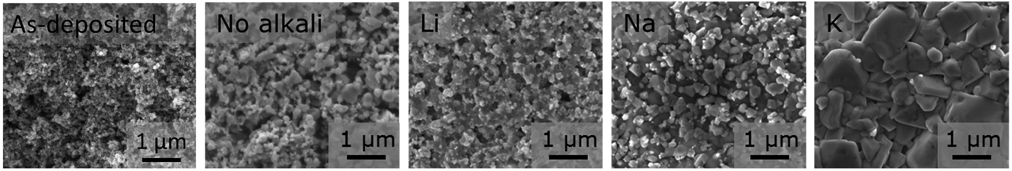 | ||
| Fig. 1 Top view SEM images of as-deposited CZTS films and films with and without alkali elements annealed at 600 °C. Large grains are seen in the K-doped samples, while smaller grains and a more porous surface structure is present in the other samples. | ||
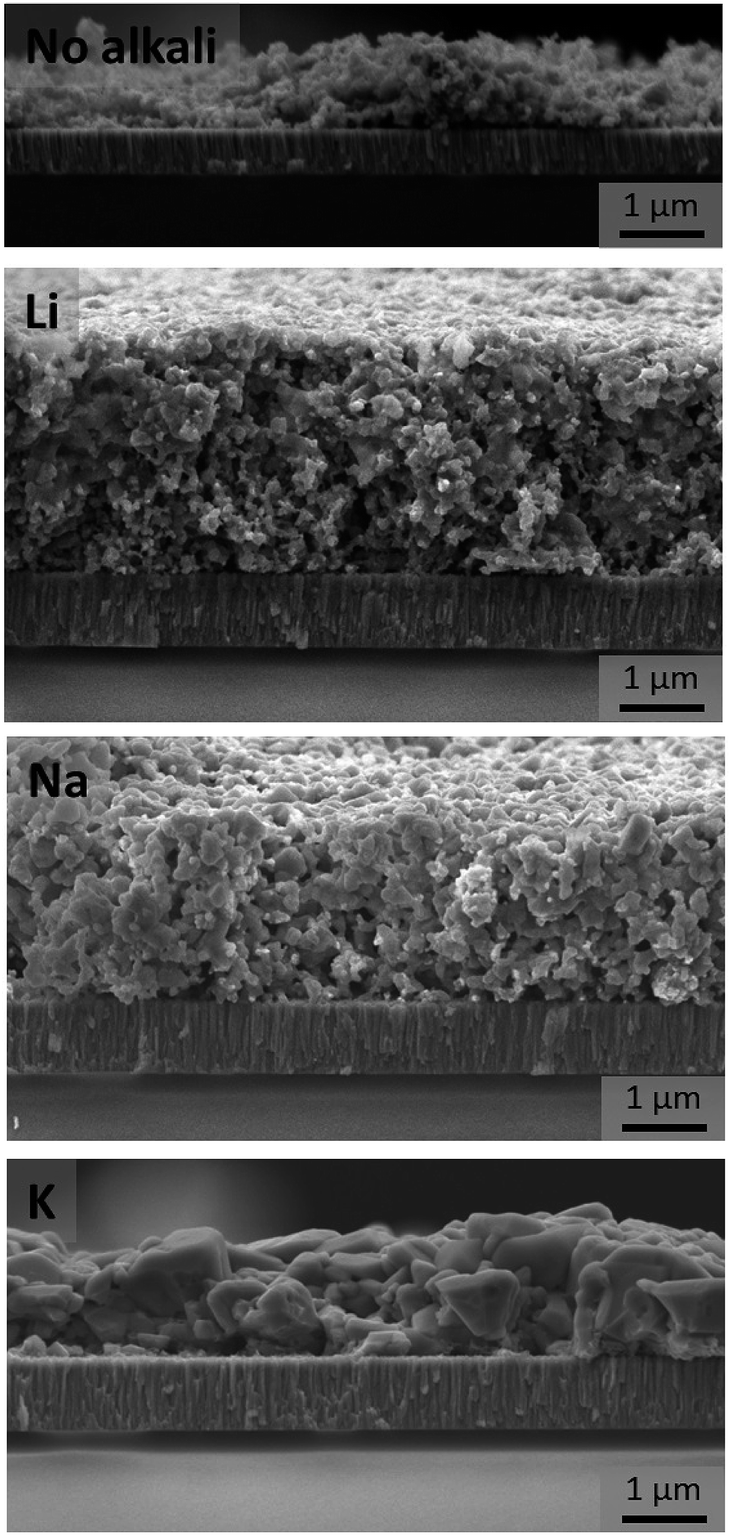 | ||
| Fig. 2 Cross-section SEM images of annealed films show large, dense grains in the cross-section of the K-doped sample, while smaller grains are observed for the un-doped, and Li- and Na-doped samples. | ||
All films had a Cu-poor and Zn-rich composition, while also being Sn-poor, as displayed in Table 1. Due to the low atomic number of Li (Z = 3), and overlapping X-ray emission lines of the other alkali elements and cations, it was challenging to quantify the exact amount of alkali elements and chloride in the annealed films. Nonetheless, after a quick water rinse, absolutely no trace amounts of alkali or chloride could be detected within the films. ICP-MS was carried out on a different batch of as-synthesized nanoparticles (about 200 mg). The results showed that the composition was Cu1.97Zn1.03SnS3.77 and Cu1.76Zn0.99SnS3.54 according to EDX and ICP-MS, respectively, suggesting that the EDX analysis overestimates the Cu-content and slightly underestimates the Sn-content. Thus the films characterized in this paper are actually even more Cu-poor than the EDX data indicates.
| Sample | Cu/(Zn + Sn) | Zn/Sn | Cu/Sn | FWHM(112) (deg) | I(112)/I(220) | Eg (eV) | PL max (eV) |
|---|---|---|---|---|---|---|---|
| No alkali | 0.73 | 1.63 | 1.92 | 0.15 | 2.69 | 1.52 | — |
| Li | 0.73 | 1.74 | 2.00 | 0.20 | 2.43 | 1.51 | 1.35 |
| Na | 0.75 | 1.70 | 2.01 | 0.15 | 2.53 | 1.52 | 1.33 |
| K | 0.80 | 1.73 | 1.89 | 0.11 | 3.64 | 1.43 | 1.33 |
The phase was characterized by Raman spectroscopy and XRD, and the respective spectra and patterns are showed in Fig. 3 and 4. Raman analysis using the 532 nm excitation wavelength laser reveals many of the CZTS peaks for all annealed samples both with and without alkali elements.15,16 The peak shift from 335 cm−1 for the as-deposited film to 338 cm−1 for the annealed films has been explained by internal compressive stress that is released during annealing.17 In Fig. 3(b), the UV laser reveals the presence of ZnS.18 This is not surprising, since the composition used did contain rather high amounts of Zn; a necessity in order to avoid the formation of any Sn–S phases at the back Mo-interface, as has also been reported elsewhere.19 The presence of SnS2 is detrimental for a solar cell, and as such ZnS is preferred.20
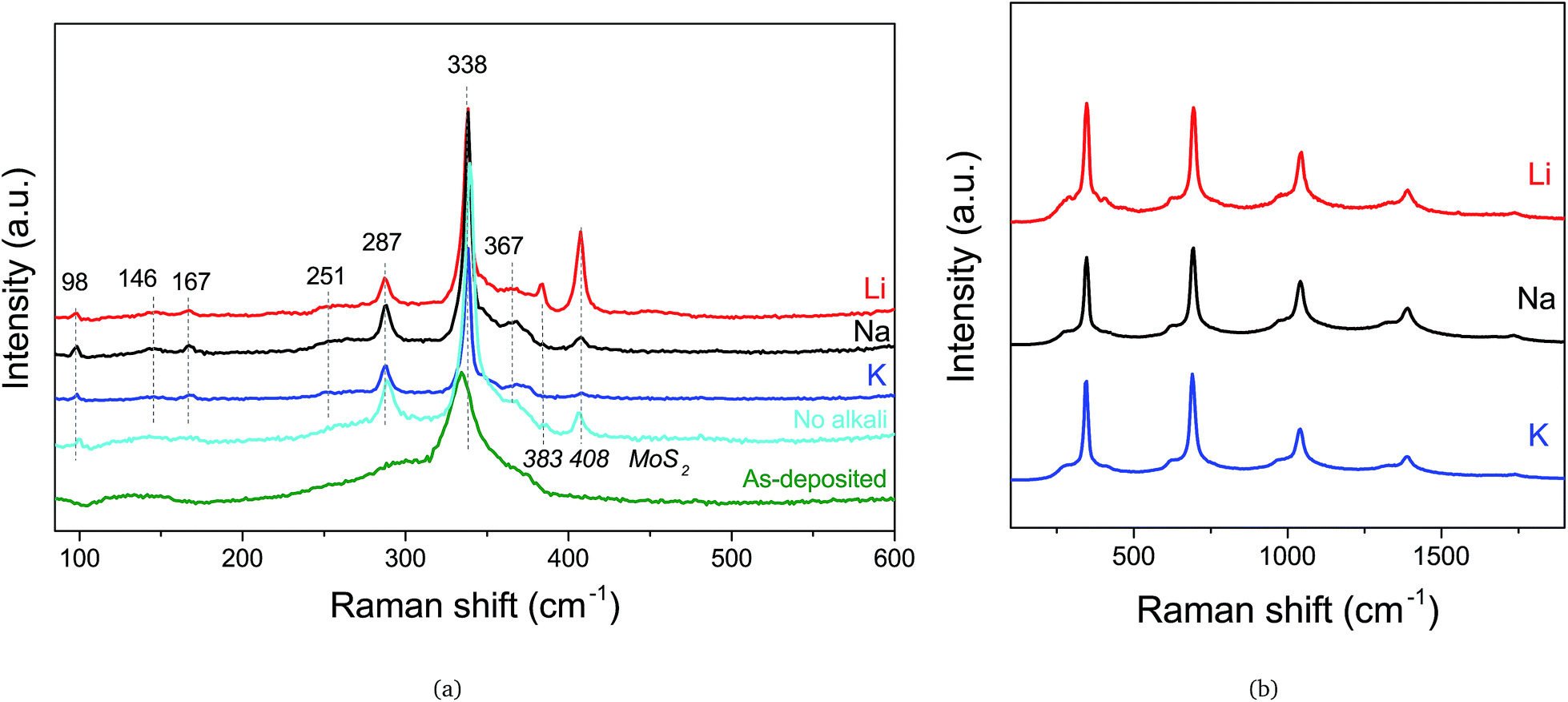 | ||
| Fig. 3 Raman spectra recorded with an (a) 532 nm laser and (b) 325 nm laser of as-deposited CZTS nanoparticle thin films, and annealed films with Li, Na, and K, and without any alkali element. The 532 nm spectra show only CZTS and MoS2 substrate peaks for annealed films, while the 325 nm spectra reveal the typical ZnS Raman peaks in the samples annealed with alkali elements. | ||
In addition to the substrate diffraction peak at 2θ = 42 degrees assigned to the Mo substrate, the XRD patterns (Fig. 4) present several of the kesterite CZTS peaks (ICSD collection code 171983), namely 23.3 (110), 28.7 (112), 29.8 (103), 33.1 (200), 37.1 (202), 38.1 (211), 45.1 (105), 47.5 (220), 56.3 (303), and 59.0 degrees (224). Only the Li-sample includes a number of unidentified peaks, which could be related to several secondary phases. No noticeable peak shifts could be detected between the different samples, as has been seen by others as a result from alkali-incorporation in the bulk of CZTS.4 However, a difference is found in the I(112)/I(220) ratio, which increases for the K-sample (Table 1), suggesting a slight preferential orientation of these CZTS films. The full width half maximum (FWHM) of the main (112) reflection changes from 0.75 degrees to 0.11 degrees for the as-deposited sample to the annealed K-sample. This indicates an increase in the crystallite size from 11 nm to 75 nm, according to the Scherrer equation when assuming no strain in the film.
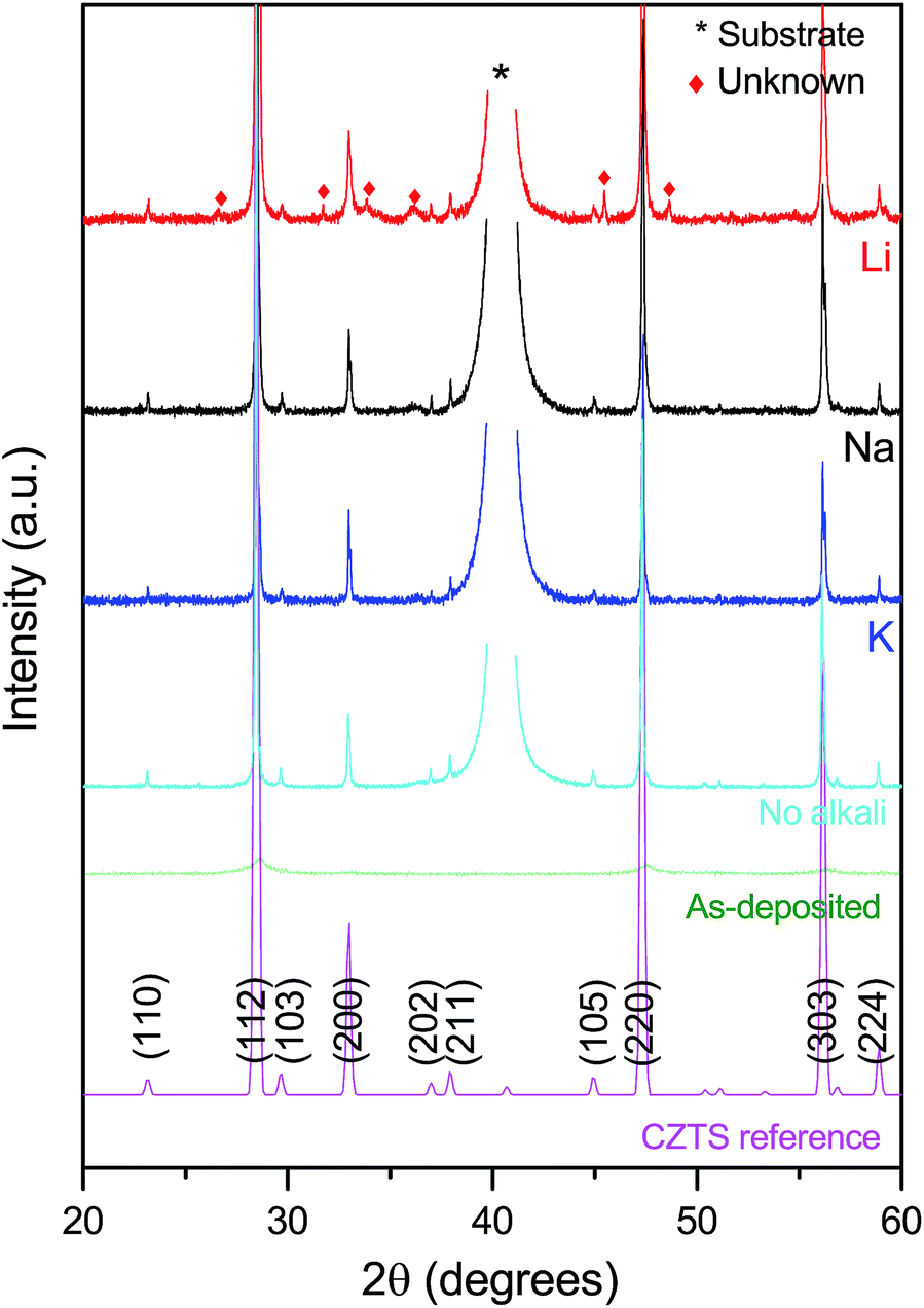 | ||
| Fig. 4 XRD patterns of as-deposited nanoparticle thin films, annealed films without an alkali element and with Li, Na, and K, as well as the CZTS reference pattern (ICSD collection code 171983). The patterns show pure-phase CZTS, with no other peaks visible (after water bath), apart from the Mo-substrate peak denoted with an asterisk, and the unidentified peaks in the Li-doped sample. | ||
Opto-electronic properties of the films were also investigated in terms of the optical band gap and photoluminescence. The equivalent absorption coefficients, F(R∞), are displayed in Fig. 5(a), and the Tauc plot ((F(R∞)hv)2 versus photon energy, hv) is showed in Fig. 5(b), where the reflectance R∞ = Rsample/Rstandard. No band gap could be extracted from an as-deposited sample, suggesting a high density of non-radiative defects. The extrapolated direct optical band gaps of the Na-, Li- and as-annealed samples were approximately 1.5 eV, while the CZTS with K was around 1.45 eV. Potassium is not expected to shift the band gap of CZTS films, whereas Li has been seen to increase the band gap of similar samples.21 All measured values remain in the range of reported values for CZTS, and we cannot explain the shift in optical absorption.
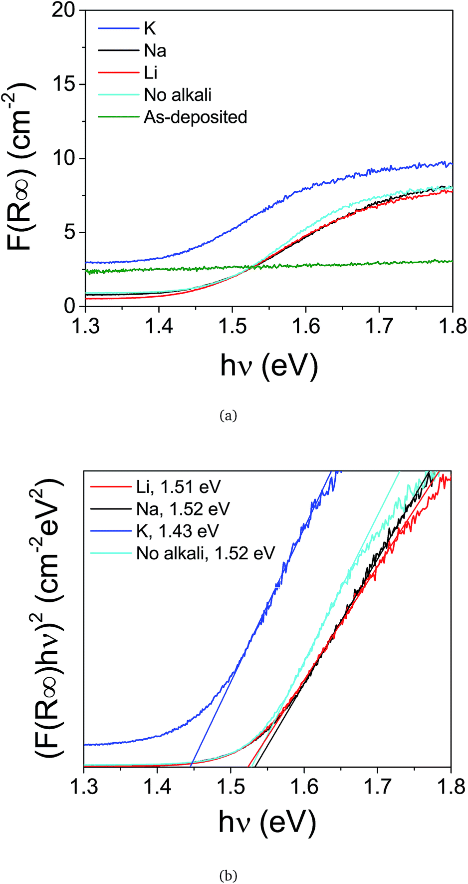 | ||
| Fig. 5 The equivalent absorption coefficients (a) and Tauc plot (b) of as-deposited and annealed thin films. The extrapolated band gap value is lowest for K, and similar for Li, Na, and no alkali used. | ||
The room-temperature photoluminescence spectrum in Fig. 6 shows the effect of alkali-incorporation on the typical photoluminescence intensity. In general, the K-samples displayed the highest intensity, closely followed by the Na-samples, whereas samples annealed without an alkali element did not show any photoluminescence signal. The increase in photoluminescence could be related to reduced interface recombination from quenching of non-radiative recombination paths in the absorber.22 Na is known to passivate grain boundary defects in CIGS,23 and reduce deep level traps in CIGS and CuInSe2.24–26 Similarly, Xin et al. saw that Li-doping increased the device efficiency of Cu2ZnSn(S,Se)4 (CZTSSe) by improving the quality of the material.27 The photoluminescence peak positions of approximately 1.35 eV listed in Table 1 are extracted based on a Gaussian fit and indicate a VOC-deficit.
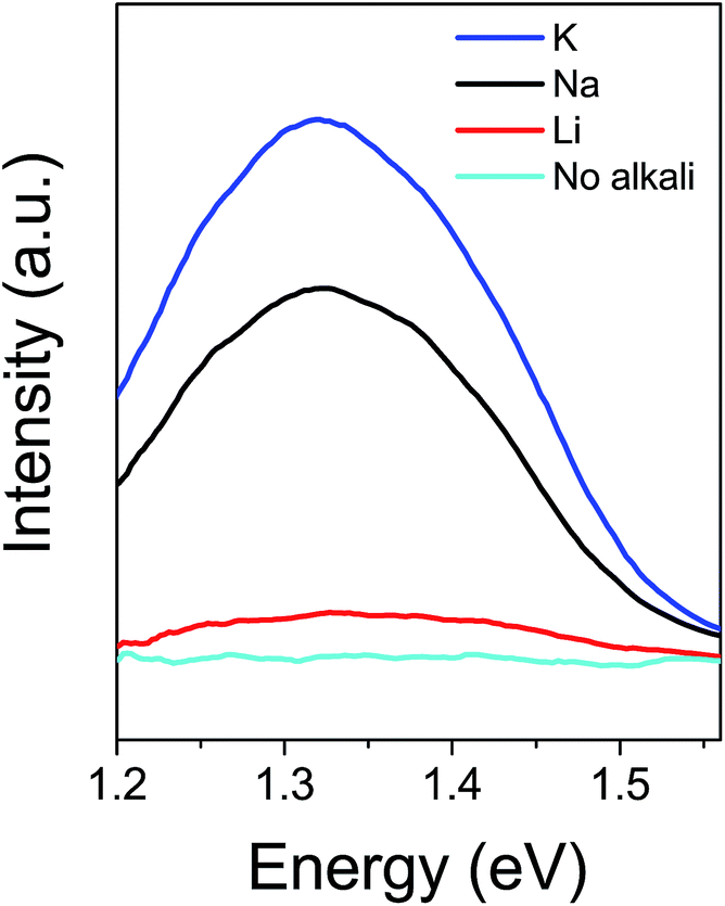 | ||
| Fig. 6 Room temperature photoluminescence spectrum (532 nm excitation wavelength) of CZTS thin films with Li, Na, and K, as well as without any alkali element, annealed at 600 °C in nitrogen and sulfur atmosphere. | ||
2.1 Proposed formation mechanism
To illustrate what happens during annealing, Fig. 7 shows a nanoscale description of grain growth. The formation mechanism is expected to occur in the following steps: as the material is heated, the residual solvent and any potential material that is coating the nanoparticles, will disappear by thermal decomposition. These species could stem from ethanol, water and amine species in the ink, as based on a thermogravimetric analysis reported earlier,13 (only without alkali elements). Once the coating is removed, particles in contact can start to merge. For as-annealed powders (Fig. 7(top)), this process was very slow, and could not be run to completeness under any annealing conditions used. On the contrary, when K is introduced, it is expected to form a reactive liquid phase, e.g. in the form of potassium sulfide, which aids merging of the particles, and the particles will sinter (Fig. 7(bottom)). As sulfur is volatile, more reactive sulfur in the form of K2Sx is advantageous. Similar approaches for grain growth in CZTS are annealing in reactive H2S gas,28,29 applying high amounts of S in the precursor ink,30 or in other ways ensuring a high partial pressure of sulfur inside the graphite box. For a more thorough description on the liquid phase mediated route, see the work by Braunger et al. which concerns CIGS and Na.31 Due to the resemblance between the Na–S and Na–Se phase diagrams, and the Na–S and K–S systems, a similar mechanism could be used to explain the increased grain growth in pure sulfide-phase CZTS systems.32–34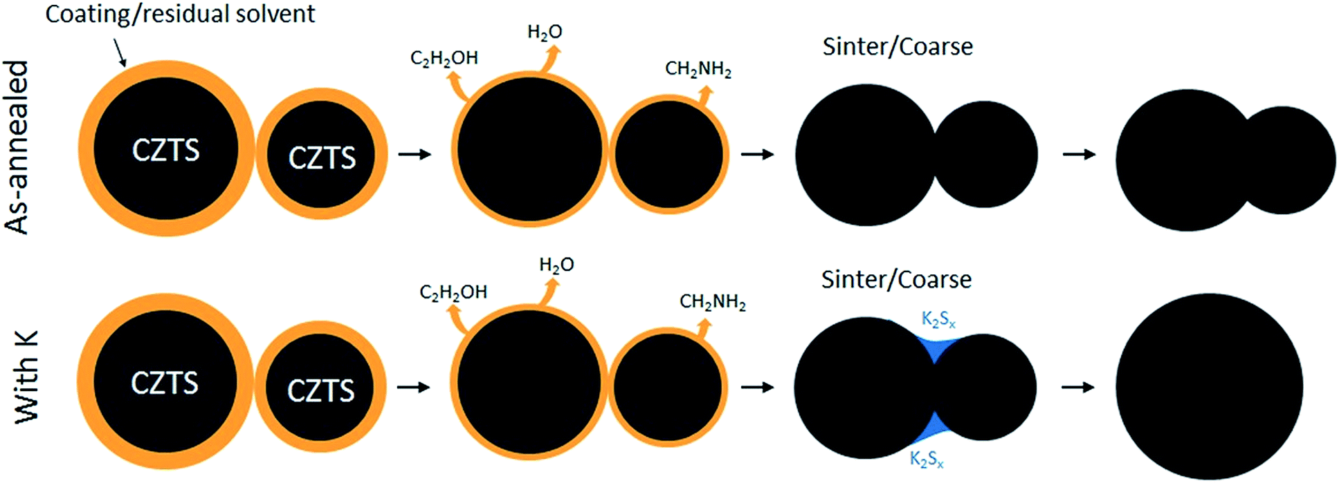 | ||
| Fig. 7 Proposed nanoscale formation mechanism for CZTS nanoparticles annealed with and without K. Without K, individual particles cannot be merged completely, and the film remains porous and small-grained. With K, a liquid phase in the form of K2Sx or similar could be formed, and it will assist the sintering of the particles. The final film will thus become more dense and with larger grains. Sketch inspired by Tiong et al.6 | ||
When comparing the phase diagrams of Li–S, Na–S, and K–S, it is clear that the temperature at which the material becomes liquid is lower in the K–S system, which could explain why more grain growth takes place in these samples.33–35 Needless to say, decreasing the annealing temperature further is relevant both from an energy-saving-perspective and to limit evaporation of volatile elements in the CZTS compound.
3 Conclusion
We have demonstrated the beneficial effect of K-inclusion in pure-sulfide CZTS nanoparticle thin films, both in terms of improved micro-structural evolution as well as improved opto-electronic properties. When including Na or Li, the film morphology becomes more dense, but the grain growth is still insufficient for achieving micron-sized grains, which is also reflected in a lower photoluminescence signal. The created thin films were Cu-poor and Zn-rich, displayed good crystallinity and no secondary phases apart from ZnS could be detected for the K-sample. A high photoluminescence signal was recorded for the K-sample, and an optical band gap of around 1.45 eV. We suggest that at elevated temperatures and with excess amount of S, potassium will form a liquid phase compound that promotes solid state diffusion and thereby enhances sintering.Conflicts of interest
There are no conflicts to declare.Acknowledgements
We greatly appreciate Niels Christian Schjødt's assistance with the ICP MS measurement. This work was supported by a grant from the Innovation Fund Denmark.References
- M. A. Green, Y. Hishikawa, W. Warta, E. D. Dunlop, D. H. Levi, J. Hohl-Ebinger and A. W. Y. Ho-Baillie, Prog. Photovoltaics Res. Appl., 2017, 25, 668–676 CrossRef.
- K. Ito, in Copper Zinc Tin Sulfide-Based Thin-Film Solar Cells, ed. K. Ito, Wiley, Nagano, Japan, 1st edn, 2015, ch. 1, pp. 3–41 Search PubMed.
- X. Liu, F. Zhou, N. Song, J. Huang, C. Yan, F. Liu, K. Sun, J. A. Stride, X. Hao and M. Green, J. Mater. Chem. A, 2015, 3, 23185–23193 CAS.
- D. Tiwari, T. Koehler, X. Lin, R. Harniman, I. Griffiths, L. Wang, D. Cherns, R. Klenk and D. J. Fermin, Chem. Mater., 2016, 28, 4991–4997 CrossRef CAS.
- Y. Kim, K. Woo, I. Kim, Y. Soo Cho, S. Jeong and J. Moon, Nanoscale, 2013, 5, 10183–10188 RSC.
- V. Tiing Tiong, Y. Zhang, J. Bell and H. Wang, RSC Adv., 2015, 5, 20178–20185 RSC.
- L. C. de Jonghe and M. N. Rahaman, in Handbook of Advanced Ceramics, ed. S. Somiya, Elsevir Inc., Berkeley, 1st edn, 2003, ch. 4, p. 187 Search PubMed.
- C. B. Carter and M. G. Norton, in Ceramic Materials: Science and Engineering, ed. C. B. Carter and M. G. Norton, Springer, New York, 1st edn, 2007, ch. 24, pp. 427–443 Search PubMed.
- T. Jiao Huang, X. Yin, C. Tang, G. Qi and H. Gong, J. Mater. Chem. A, 2015, 3, 17788–17796 Search PubMed.
- H. Zhou, T.-B. Song, W.-C. Hsu, S. Luo, S. Ye, H.-S. Duan, C.-J. Hsu, W. Yang and Y. Yang, J. Am. Chem. Soc., 2013, 135, 15998–16001 CrossRef CAS PubMed.
- A. Carrete, A. Shavel, X. Fontané, J. Montserrat, J. Fan, M. Ibáñez, E. Saucedo, A. Pérez-Rodríguez and A. Cabot, J. Am. Chem. Soc., 2013, 135, 15982–15985 CrossRef CAS PubMed.
- N. Mirbagheri, S. Engberg, A. Crovetto, S. B. Simonsen, O. Hansen, Y. M. Lam and J. Schou, Nanotechnology, 2016, 27, 185603 CrossRef CAS PubMed.
- S. Engberg, K. Agersted, A. Crovetto, O. Hansen, Y. M. Lam and J. Schou, Thin Solid Films, 2017, 628, 163–169 CrossRef CAS.
- S. Davidsdottir, K. Dirscherl, S. Canulescu, R. Shabadi and R. Ambat, RSC Adv., 2013, 3, 23296–23302 RSC.
- M. Dimitrievska, H. Xie, A. Fairbrother, X. Fontané, G. Gurieva, E. Saucedo, A. Pérez-Rodríguez, S. Schorr and V. Izquierdo-Roca, Appl. Phys. Lett., 2014, 105, 0–5 CrossRef CAS.
- X. Fontané, E. Saucedo, J. R. Morante, D. M. Berg, P. J. Dale, S. Siebentritt, X. Fontané and E. Saucedo, Appl. Phys. Lett., 2011, 98, 1–4 CrossRef.
- H. Yoo and J. Kim, Sol. Energy Mater. Sol. Cells, 2011, 95, 239–244 CrossRef CAS.
- A. Fairbrother, V. Izquierdo-Roca, X. Fontané, M. Ibáñez, A. Cabot, E. Saucedo and A. Pérez-Rodréguez, CrystEngComm, 2014, 16(20), 4120–4125 RSC.
- Y. Ren, M. Richter, J. Keller, A. Redinger, T. Unold, O. Donzel-gargand, J. J. S. Scragg and C. Platzer-Björkman, ACS Energy Lett., 2017, 2, 1–6 CrossRef.
- M. Kumar, A. Dubey, N. Adhikari, S. Venkatesan and Q. Qiao, Energy Environ. Sci., 2015, 8, 3134–3159 CAS.
- A. Lafond, C. Guillor-Deudon, J. Vidal, M. Paris, C. La and S. Jobic, Inorg. Chem., 2017, 56, 2712–2721 CrossRef CAS PubMed.
- T. Gershon, B. Shin, N. Bojarczuk, M. Hopstaken, D. B. Mitzi and S. Guha, Adv. Energy Mater., 2016, 5, 1–8 Search PubMed.
- L. Kronik, U. Rau, J. Francois Guillemoles, D. Braunger, H. W. Schock and D. Cahen, Thin Solid Films, 2000, 361, 353–359 CrossRef.
- D. W. Niles, J. Vac. Sci. Technol., A, 1997, 15, 3044 CAS.
- M. Igalson, A. Kubiaczyk, P. Zabierowski and M. Bodegard, Thin Solid Films, 2001, 387, 225–227 CrossRef CAS.
- S. Wei, S. B. Zhang and A. Zunger, J. Appl. Phys., 1999, 85, 7214–7218 CrossRef CAS.
- H. Xin, S. M. Vorpahl, A. D. Collard, I. L. Braly, A. R. Uhl, B. W. Krueger, D. S. Ginger and H. W. Hillhouse, Phys. Chem. Chem. Phys., 2015, 17, 23859–23866 RSC.
- K. Woo, Y. Kim and J. Moon, Energy Environ. Sci., 2012, 5, 5340 CAS.
- K. Maeda, K. Tanaka, Y. Fukui and H. Uchiki, Jpn. J. Appl. Phys., 2011, 50, 1–4 CrossRef.
- G. Larramona, S. Bourdais, A. Jacob, C. Choné, T. Muto, Y. Cuccaro, B. Delatouche, C. Moisan, D. Péré and G. Dennler, RSC Adv., 2014, 4, 14655 RSC.
- D. Braunger, D. Hariskos, G. Bilger, U. Rau and H. W. Schock, Thin Solid Films, 2000, 362, 161–166 CrossRef.
- J. Sangster and A. D. Pelton, J. Phase Equilib., 1997, 18, 185–189 CrossRef CAS.
- J. Sangster and A. D. Pelton, J. Phase Equilib., 1997, 18, 89–96 CrossRef CAS.
- J. Sangster and A. D. Pelton, J. Phase Equilib., 1997, 18, 82–88 CrossRef CAS.
- H. Okamoto, J. Phase Equilib., 1995, 16, 94–97 CrossRef CAS.
| This journal is © The Royal Society of Chemistry 2018 |