
 Open Access Article
 This Open Access Article is licensed under a Creative Commons Attribution-Non Commercial 3.0 Unported Licence
The role of thermal annealing on the microstructures of (Ti, Fe)-alloyed Si thin-film anodes for high-performance Li-ion batteries†
Minsub Oha,
Ilwhan Kimab,
Hoo-Jeong Leea,
Seungmin Hyun‡
*b and
Chiwon Kang‡*a
aSchool of Advanced Materials Science and Engineering, Sungkyunkwan University, Suwon, Republic of Korea. E-mail: chiwonkang@skku.edu
bNano-Convergence Mechanical Systems Research Division, Korea Institute of Machinery and Materials (KIMM), Daejeon, Republic of Korea. E-mail: hyun@kimm.re.kr
First published on 1st March 2018
Abstract
Here, we studied the effect of thermal annealing on the microstructure and cyclic stability of a (Ti, Fe)-alloyed Si thin-film fabricated by a simple sputtering deposition method for Li-ion battery (LIB) anodes. The anode samples annealed at different temperatures (300–600 °C) were subjected to microstructure analysis and LIB performance test. The (Ti, Fe)-alloyed Si thin-film anode delivered a high capacity of 1563 mA h g−1 for 100 cycles at 0.1 A g−1 with nearly 100% capacity retention. Post-mortem analysis using field emission scanning electron microscopy (FESEM) and transmission electron microscopy (TEM) disclosed the microstructural changes of the cycled anodes, revealing that (Ti, Fe) silicides served as a structural buffer against the large volume change of active Si during cycling for enhanced LIB performance.
Introduction
The ever-increasing demand for high energy density lithium-ion batteries (LIBs) for large-scale energy storage systems (e.g., electric vehicles) has led to an expansion in new developmental efforts for high-capacity anode materials.1 However, commercially available graphite anodes have their critical drawback of a low theoretical specific capacity (372 mA h g−1), hindering their further implementation into advanced energy storage systems.1 In this context, Si has drawn much attention as a promising anode material owing to its exceptional theoretical capacity [approximately 4200 mA h g−1 (Si + 4.4Li+ + 4.4e− ↔ SiLi4.4)], abundancy and low-cost.2 Despite these unique features of Si materials, the most serious problem with Si is poor cyclic stability, arising from a large volume change occurring due to extensive reactions between Si and Li during cycling. Such a volume change usually leads to pulverization issue among Si nanomaterials, which is accompanied by their electrical contact loss among Si particles, finally resulting in capacity fading.3,4To overcome this limitation, the integration of inactive transition metals into nanostructured Si to form Si-based alloys,5–14 nanostructured Si/carbon-based composites (e.g., graphite/nanostructured Si/carbon15,16 and nanosilicon cluster-SiOx–C17), and nanostructured Si/SiO2![[thin space (1/6-em)]](https://www.rsc.org/images/entities/char_2009.gif) 18 have recently garnered great attention for good, stable cycling performance with high specific capacities. Among these nanostructured Si-based anode materials, we especially focus on the transition metal/Si-based alloy nanocomposite anode structure. In this structure, inactive transition metal silicides could serve as cushioning media by buffering against the extent of volume changes of the Si active materials during cycling, therefore lending a high structural integrity to the anode structure. Furthermore, the presence of transition metal silicides could enhance the electrical conductivity in the anode structure. Although several studies based on such alloyed Si anodes have been reported, processing methods used to grow the nanostructured Si usually require complicated thermo chemical processing steps at high temperatures5,6 and the fabrication processings need safe handling of metal powders.8,10,19 Nevertheless, few study has been done into a simple fabrication method of Si–silicide nanocomposite anodes for advanced Li-ion battery. Sputtering deposition method could be one of viable approaches to fabricate (Ti, Fe)-alloyed Si thin-film anodes with high-efficiency and nearly accurate stoichiometric composition of the anode structure.20–22 Furthermore, the sputtering method is advantageous to investigate the fundamental study on microstructural variation induced by process condition and ex situ analysis with different levels of state of charge (SOC) owing to the homogeneous composition in the thin film.23
18 have recently garnered great attention for good, stable cycling performance with high specific capacities. Among these nanostructured Si-based anode materials, we especially focus on the transition metal/Si-based alloy nanocomposite anode structure. In this structure, inactive transition metal silicides could serve as cushioning media by buffering against the extent of volume changes of the Si active materials during cycling, therefore lending a high structural integrity to the anode structure. Furthermore, the presence of transition metal silicides could enhance the electrical conductivity in the anode structure. Although several studies based on such alloyed Si anodes have been reported, processing methods used to grow the nanostructured Si usually require complicated thermo chemical processing steps at high temperatures5,6 and the fabrication processings need safe handling of metal powders.8,10,19 Nevertheless, few study has been done into a simple fabrication method of Si–silicide nanocomposite anodes for advanced Li-ion battery. Sputtering deposition method could be one of viable approaches to fabricate (Ti, Fe)-alloyed Si thin-film anodes with high-efficiency and nearly accurate stoichiometric composition of the anode structure.20–22 Furthermore, the sputtering method is advantageous to investigate the fundamental study on microstructural variation induced by process condition and ex situ analysis with different levels of state of charge (SOC) owing to the homogeneous composition in the thin film.23
Here, we designed and fabricated (Ti, Fe)-alloyed Si thin-film anode for high-performance LIB. In this anode, (Ti, Fe) silicides served to guard against volume variation induced by Li–Si reaction during cycling, leading to a high capacity of above 1500 mA h g−1 for 100 cycles with a capacity retention of approximately 100%. We previously fabricated a Si-based alloy thin-film anode via co-sputtering and demonstrated excellent LIB performance.23 Furthermore, we investigated the mechanism for the stable microstructure of the anode to acquire the long-term cycling stability through analytical techniques. In the present study, we focused on the roles of crystalline metal silicides (TiFeSi2 and (Ti, Fe) silicides) synthesized by thermal annealing to structurally guard against large volume variation of active Si during cycling. Furthermore, using structural analytical techniques, we disclosed that behind the excellent LIB performance in this present study were electrochemically derived microstructural rearrangement of the metal silicide phases and morphological regeneration during cycling.
Experimental
Fabrication of (Ti, Fe)-alloyed Si thin-film
(Ti, Fe)-alloyed Si thin-film was deposited on a stainless steel foil (i.e., 18 μm thick) substrate at room temperature using Si, Ti and Fe targets (2 inch diameter) in a radio-frequency (RF) magnetron sputtering system. The power densities applied to the Si, Ti and Fe targets are 9.87, 1.18 and 1.23 W cm−2, respectively. The composition (at%) of the (Ti, Fe)-alloyed Si thin-film was approximately 80:10:10 (=Si:Ti:Fe), according to energy-dispersive X-ray spectroscopy (EDS) data (see Fig. S1 in the ESI†). Furthermore, our EDS results were averaged for 6 conditions of the RF power densities for the Si target and analyzed for 5 times each (see Table S1†). Based on the very low standard deviation (i.e., approximately 1–2%) from the mean value, it is quite certain that our EDS data are consistent. The film thickness was found to be around 200 nm. To improve adhesion, the stainless steel substrate was subjected to plasma treatment onto it using an radio-frequency (RF) plasma processing system; subsequently, Ta layer with a thickness of 50 nm was deposited as an adhesion layer between stainless steel and (Ti, Fe)-alloyed Si thin-film. Lastly, the samples were post-annealed at from 100 to 800 °C for 1 h under vacuum ambient (about 10−7 torr) using a high vacuum tube furnace.
Electrochemical analysis
The (Ti, Fe)-alloyed Si thin-film served as a working electrode, whereas Li foil worked as a reference and counter electrode. Also, a commercial monolayer polypropylene (PP) (Celgard® 2400) was used as a separator. The electrolyte was 1 M LiPF6 dissolved in a 4:6 volume ratio mixture of fluoro-ethylene carbonate (FEC) and diethyl carbonate (DEC). All these components were assembled in a 2032 type coin-cell in an Ar-filled glove box controlling oxygen and moisture levels less than 0.1 ppm, respectively. Galvanostatic charge–discharge cycling measurements for the cell were conducted in a voltage range of 0.05 to 2.5 V (vs. Li/Li+) at current densities ranging from 0.1 to 10 A g−1. Cyclic voltammetry (CV) was performed in a voltage range of 0.05 to 2.5 V versus Li/Li+ at a scanning rate of 1 mV s−1.
Morphological and microstructural characterization
Microstructural evolution of the (Ti, Fe)-alloyed Si thin-film annealed at the different temperatures (100–800 °C) was identified by X-ray Diffraction (XRD, X'pert APD) analysis, using Cu Kα radiation at 50 kV and 25 mA. Microstructural evolution of the (Ti, Fe)-alloyed Si thin-film annealed at the different temperatures (100–800 °C) was identified by X-ray Diffraction (XRD, X'pert APD) analysis, using Cu Kα radiation at 50 kV and 25 mA. For the XRD measurement, (Ti, Fe)-alloyed Si thin-film was deposited on a SiOx/Si wafer substrate (instead of the stainless steel foil) and then thermally treated to avoid any problem with roughness of the stainless steel substrate. Furthermore, we slightly tilted the SiOx/Si wafer substrate to remove Si peak corresponding to the substrate from the XRD patterns. Micro-/nanoscaled structural changes in the (Ti, Fe)-alloyed Si thin-film were observed by field emission scanning electron microscopy (FESEM, Magellan400) and transmission electron microscopy (TEM, JEM ARM 2100F, operating at 80 keV and 200 keV). In addition, we prepared samples for cross-sectional TEM images by using gallium (Ga)-based focused ion beam-scanning electron microscopy (FIB-SEM, Helios Nanolab 450 F1). Platinum (Pt) was coated on the samples to avoid any problem with the sample's morphological change caused by ion-beam bombardment.Results and discussion
Microstructural evolution and morphological change
The composition of the ternary material we used for this study was Si:Fe:Ti = 80:10:10 (at%), marked by the red “X” point inside the ternary phase diagram shown in Fig. S2.† The phase diagram predicts that Si and various (Ti, Fe) silicides coexist depending on annealing conditions. One should note that there have been several reports on the beneficial properties of the TiFeSi2 phase as an electrically conducting and mechanically buffering material.10,24–26
Fig. 1 demonstrates the XRD curves of the (Ti, Fe)-alloyed Si thin-film samples annealed at the different temperatures up to 800 °C. Below 400 °C, peaks from Ta, the underlayer, are the only dominant ones, suggesting no crystalline (Ti, Fe) silicide (TiSi2, FeSi2 and TiFeSi2) was formed by annealing at the low temperatures. The peaks at 2θ = 41.9° and 48.3° corresponding to the crystal planes of orthorhombic TiSi2 (JCPDS #85-0879) and tetragonal FeSi2 (JCPDS #35-0822) arose upon annealing at 500 °C, respectively. Upon annealing at higher temperatures (700 and 800 °C), the peaks become much stronger and other silicide peaks also appear while the Ta peaks disappear, suggesting that the Ta underlayer has reacted with the anode.
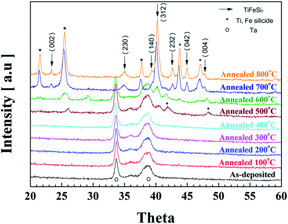 | ||
| Fig. 1 X-ray diffraction patterns representing the structural phase evolution in the (Ti, Fe)-alloyed Si thin-film samples annealed at the different temperatures. | ||
Fig. 2 demonstrates cross-sectional TEM images showing microstructural changes in the (Ti, Fe)-alloyed Si thin-film samples annealed at temperatures up to 500 °C. The as-deposited and 300 °C-annealed samples appear amorphous (both in image and electron diffraction), consistent with the XRD results. However, high resolution (HR)-TEM, shown in Fig. S3(b),† discloses some short-range ordering in the 300 °C-annealed sample, compared to the amorphous structure of the as-deposited sample (Fig. S3(a)†). The 400 °C-annealed sample shows that the amorphous film has transformed into nanocrystalline one. The electron diffraction pattern, shown in the inset, shows several rings, of which the radii are consistent with the plane spacings of (Ti, Fe)-silicides and TiFeSi2. Upon annealing at 500 °C, some larger grains have formed and strong spots have emerged in the electron diffraction pattern. This result indicates that the film was grown amorphous initially and crystallized upon annealing at a temperature between 400 and 500 °C. This result is mostly in parallel with that of the XRD analysis except that the actual crystallization took place about 100 °C lower than the XRD analysis, suggesting that XRD could not be sensitive enough to detect the formation of a nanocrystalline structure.
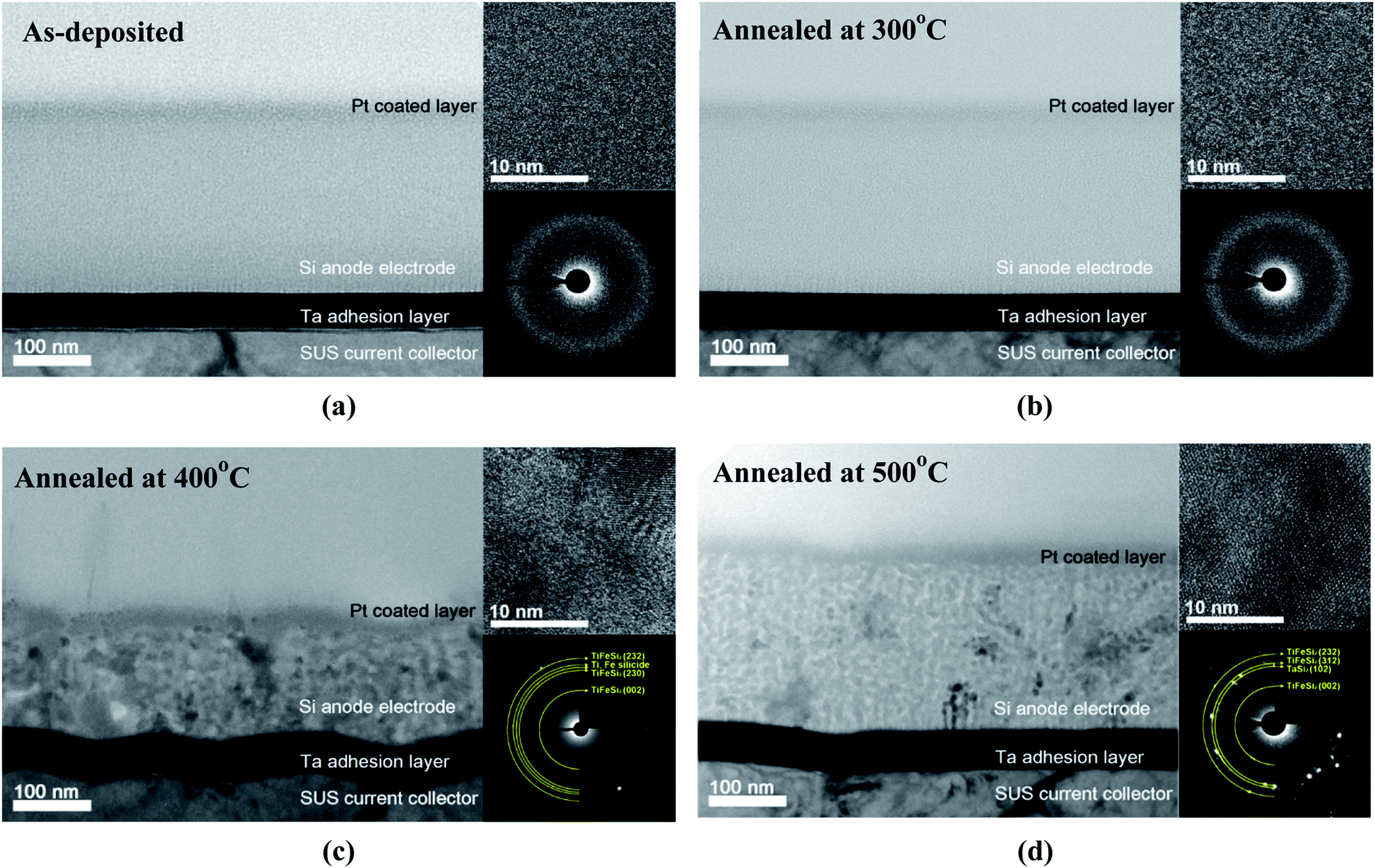 | ||
| Fig. 2 Bright field (BF) TEM images illustrating the microstructural evolution of the (Ti, Fe)-alloyed Si thin-film samples annealed at the different temperatures. The inset images of each BF TEM image are corresponding to high-resolution electron and electron diffraction pattern images, respectively. | ||
Electrochemical characterization
We explored the effects of the post annealing process on the electrochemical performance of the (Ti, Fe)-alloyed Si thin-film anode, as shown in Fig. 3(a). Fig. 3(a) compares the voltage profiles of the 100 cycled samples annealed at different temperatures up to 600 °C. The (Ti, Fe)-alloyed Si thin-film anode exhibits a typical voltage profile of an amorphous structure, manifested by the gradual decrease (ranging from ∼0.25 to 0.01 V) during discharging process (lithiation) and increase (from 0.2 to 0.6 V) during charging process (delithiation). (Ti, Fe)-alloyed Si thin film reaction of the alloy during insertion/deinsertion or lithiation/delithiation can be expressed as follows: Si + xLi+ + xe− ↔ SiLix, x can be theoretically up to 4.4.2 These results are in parallel with those of the cyclic voltammetry (CV) curves, shown in Fig. 3(b), two main broad cathodic peaks appearing at ∼0.25 and below 0.1 V, respectively, which correspond to the formation of a series of LiSix alloys. For anodic reactions, two broad anodic peaks appearing at ∼0.4 and ∼0.6 V are related to the phase transformation from LiSix alloys to (possibly, amorphous) Si. The plots of differential capacity vs potential derived from the voltage profiles [Fig. 3(a)] corroborate the results of the CV curves, as presented in Fig. S4.†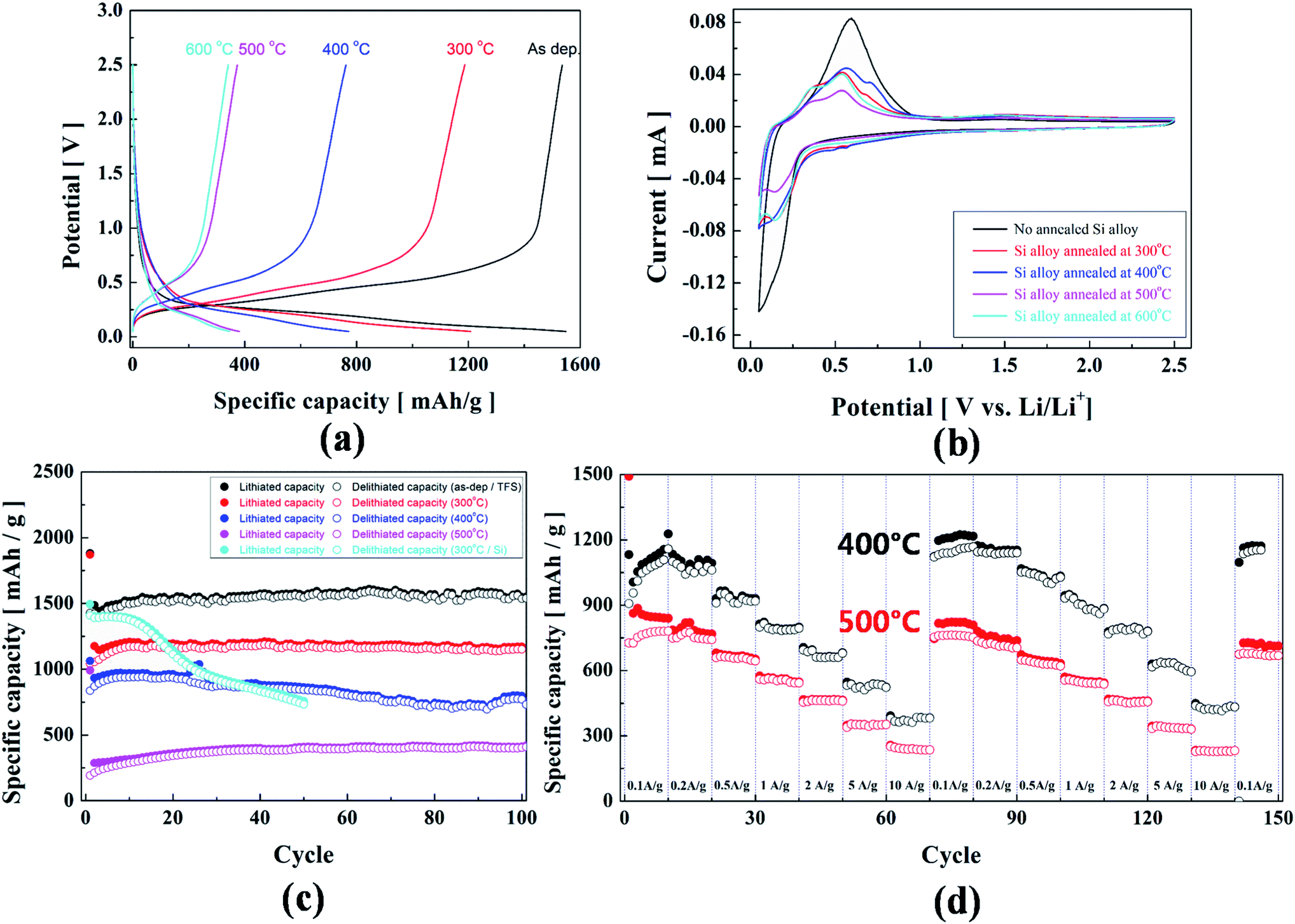 | ||
| Fig. 3 Li-ion battery performance of the (Ti, Fe)-alloyed Si thin-film anode samples annealed at the different temperatures: (a) potential profile vs. specific capacity at 0.1 A g−1, (b) cyclic voltammetry (CV) curves, (c) cycling stability, and (d) C-rate capability. | ||
In Fig. 3(c), the cyclic performance up to 100 cycles at a current density of 0.5 A g−1 clearly demonstrates a specific capacity retention of ∼100% with a high specific capacity of 1563 mA h g−1 after 100 cycles (for as-deposited sample). Furthermore, the cyclic performance data demonstrate on average 65% coulombic efficiency (CE) during 1st cycle for all the samples annealed up to 600 °C. This problem has also been observed in previous reports on Si-based anodes.25,26 The initial low CE has been ascribed to the formation of solid electrolyte interphase (SEI) on the surface of the (Ti, Fe)-alloyed Si thin-film anode and a local loss of electrical contact caused by volumetric variation of the anode.23,27 Moreover, Fig. 3(d) demonstrates the excellent cycling performance of the LIB cell for the (Ti, Fe)-alloyed Si thin-film samples annealed at 400 and 500 °C as a function of current density. The initial average specific capacity of the 400 °C annealed sample (1073 mA h g−1 at 0.1 A g−1, after running through 10 A g−1) is recovered to a value of 1150 mA h g−1, close to the initial capacity. Such high C-rate capability is mainly ascribed to the excellent structural stability of the (Ti, Fe)-alloyed Si thin-film anode, implying the inactive phases of (Ti, Fe)-silicides could play a crucial role in retaining the structural stability during cycling.
Post-mortem analysis of the (Ti, Fe)-alloyed Si thin-film anode
We conducted post-mortem study on the (Ti, Fe)-alloyed Si thin-film anode samples to observe morphological and microstructural changes through lithiation/delithiation. Fig. 4 shows the FE-SEM images of the surface morphology of the pristine and 100 cycled anode samples annealed at different temperatures ranging from 300 to 600 °C. The pristine samples, presented in Fig. 4 (left panel), display a rough surface with some pores, suggestive of the results of silicide reactions in the films. The images shown at the right panel of Fig. 4 reveal the surface of the samples after 100 cycles at the completely-lithiated state (SOC 0), disclosing a high density of bumps which appear to arise from volume expansion due to lithiation. Comparing with the images of 50 cycled samples (shown in Fig. S5†) discloses almost no difference from those of the 100 cycled samples, indicating that the films underwent a quite stable cyclic transformation during lithiation/delithiation processes. In addition, the films revealed no evidence of severe pulverization, contrast to their pure Si film counterpart in our previous study.23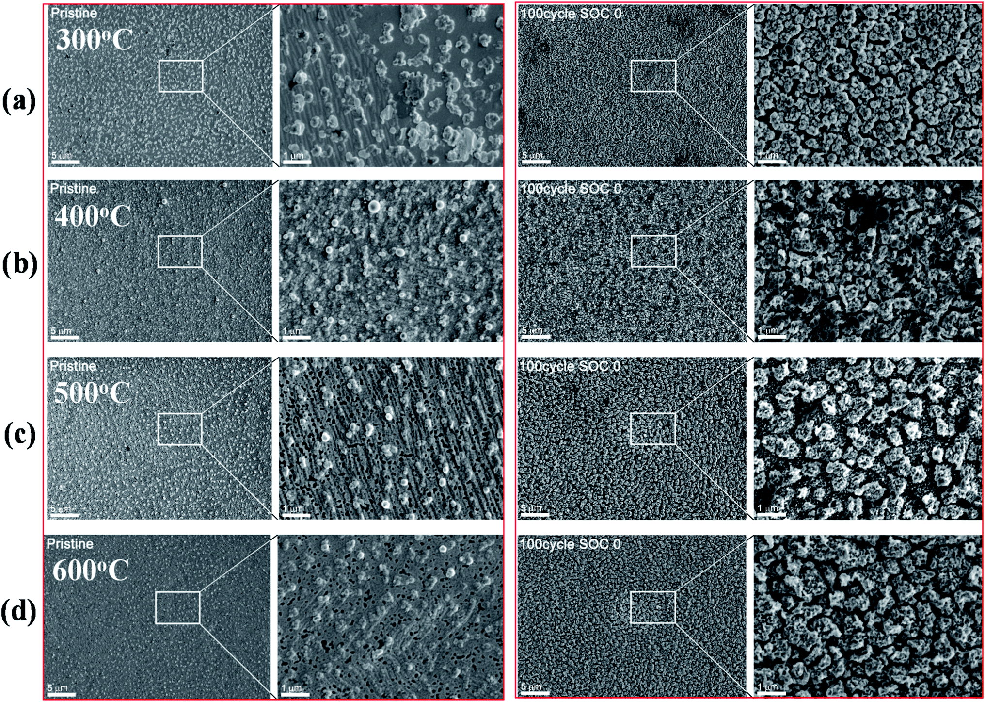 | ||
| Fig. 4 FESEM images showing surface morphological changes for the pristine and 100 cycled samples annealed at different temperatures. | ||
To understand materials reaction occurring during lithiation/delithiation cycles, we carried out in-depth TEM analysis for lithiated and delithiated samples after 25 cycles and compared the images. Fig. 5 shows the set of images obtained from the analysis [bright field (BF) electron micrographs (left), high-angle annular-dark-field (HAADF) images and elemental maps (right), electron diffraction and high resolution electron micrographs (inset)] for four sets of the samples (annealed at different temperatures, 300–600 °C). Comparing the results from the four sets of the samples helps us understand how differently the samples with different microstructures owing to annealing at the different temperatures have responded to lithiation/delithiation cylces: the segregation of Si becomes more pronounced in a sample annealed at a higher temperature.
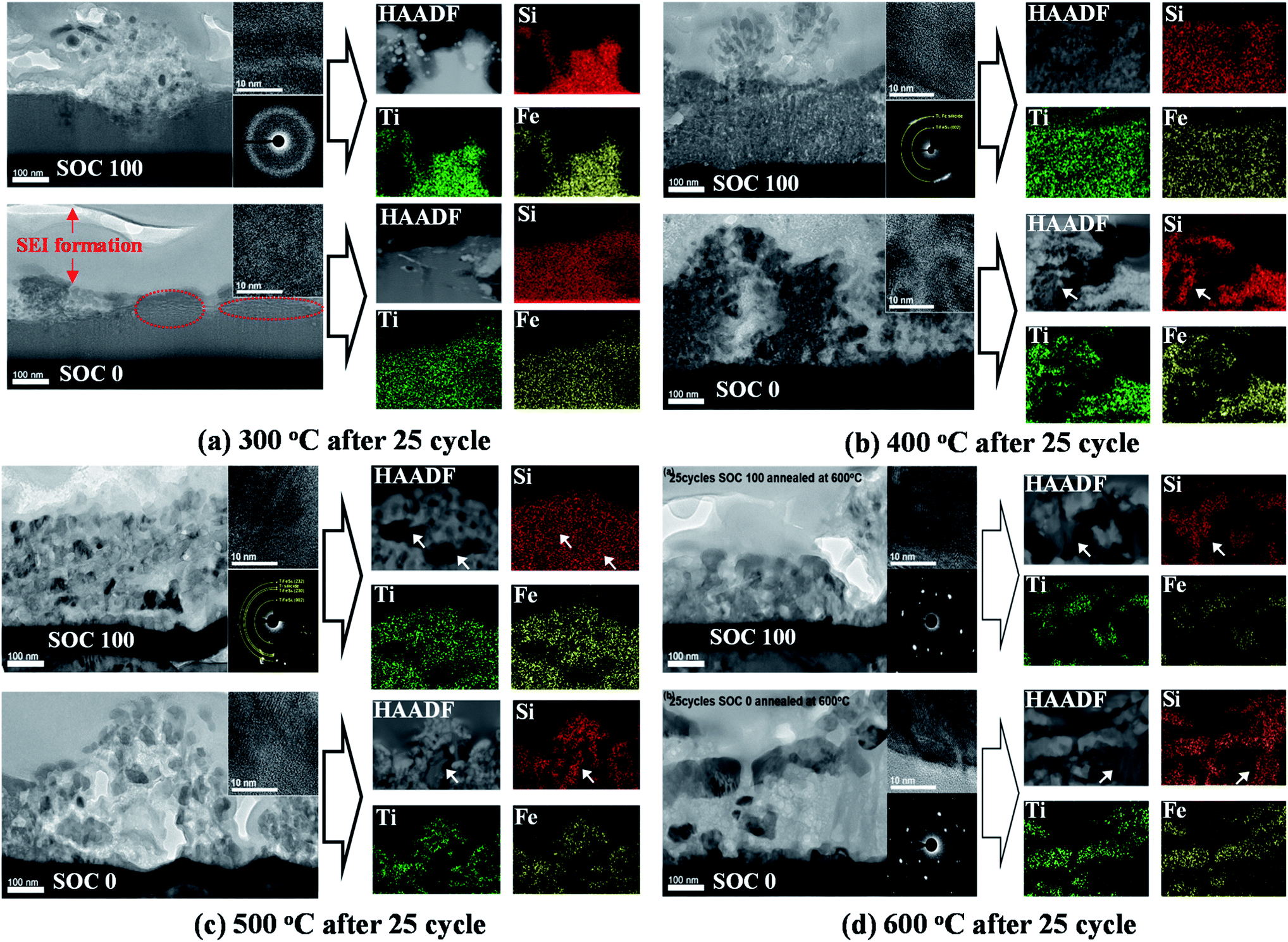 | ||
| Fig. 5 In-depth TEM analysis for the microstructural changes in the 25 cycled samples, in the state of complete lithiation (SOC 0) and delithiation (SOC 100), annealed at the different temperatures ranging from 300 to 600 °C: (left) cross-sectional bright field (BF) TEM images of the samples including the insets of (HR)-TEM images and electron diffraction patterns and (right) the corresponding HAADF images and elemental maps for the main constituents (i.e., Si, Ti and Fe). | ||
For the 300 °C annealed sample, silicidation processing has proceeded to the least degree among the four samples (see Fig. 5(a)), with some short-range ordering clusters of the (Ti, Fe)-alloyed Si thin-film anode samples. The elemental maps of the lithiated and delithiated samples disclose homogeneous distribution of the main constituents (i.e., Si, Ti, and Fe), suggesting that there may be no noticeable elemental segregation upon charging cycles. However, it should be noted that a careful analysis of the bright-field image reveals the presence of a ripple-like pattern [see the region in the red circle in Fig. 5(a) (SOC 0)]. In our previous study on the analysis on the as-deposited amorphous (Ti, Fe)-alloyed Si thin-film anode, we also observed such a ripple-like pattern, unfolding that the pattern arises from Si segregation from the alloy as Si diffuses in/out to react with Li during charging cycles. This result suggests that while the sample does not show any disruptive morphological changes, some elemental segregation at the nanoscale such as ripple-like pattern took place. Furthermore, the top bright region [indicated by the red arrow in Fig. 5(a) (SOC 0)] of the (Ti, Fe)-alloyed Si thin-film anode manifests solid electrolyte interphase (SEI) layer, in which the organic liquid electrolyte is decomposed on the surface of the active Si.28
For the 400 °C annealed sample, in which the silicidation has proceeded much and small grains of silicides have formed (see Fig. 5(b)), lithiation appears to have prompted some drastic change in morphology with formation of hillrocks and voids. A careful examination of the elemental maps (right) discloses a pocket that displays only Si (see the arrow). Considering that TEM is incapable of Li detection and that Si is the active element to react with Li, we suggest that the region be Li silicide (Si–Lix). This result suggests that as Si atoms react with incoming Li+ ions during lithiation, some of Si have been segregated and formed a pocket of Li silicide. In addition, the appearance of the morphology around the Li silicide region hints that as the Li silicide region formed from the inside of the film and expanded, the surrounding (Ti, Fe) silicide grains enveloped the region, serving as a structural buffer and thus preventing from drastic pulverization. Next, upon delithiation (see the top images), the film almost returned to the initial microstructure, a film with a uniform thickness. An interesting aspect is that such a pocket containing Si only is not found any more, which means that as Li ions drew away, Si also diffused back among the (Ti, Fe) silicide grains.
For the samples annealed at higher temperatures (i.e., 500 and 600 °C) as presented in Fig. 5(c) and (d), the trend is overall similar: morphological changes (the formation of some flakes and slits in the (Ti, Fe)-alloyed Si thin-film), Si segregation (formation of Li silicide areas) and crystalline metal silicides (TiFeSi2 and (Ti, Fe) silicides). Such morphological and crystalline changes created a free-space to buffer against the volume variations derived from pure Si active materials during cyclings, thus enhancing cycling stability. However, it should be also noted that the Si pockets have not disappeared upon delithiation, which suggests that the formation of Si pockets is now irreversible (see the arrow). Another interesting aspect is that the grains of (Ti, Fe) silicides appear to have grown larger upon charging cycles.
In summary, our in-depth TEM analysis for the sample offers insight into the lithiation/delithiation mechanism leading to the excellent cycling stability. For the sample annealed at the lower temperature (300 °C), the ripple-patterned (Ti, Fe) silicides formed to serve as a structural buffer against the large volume change of active Si for Si–Lix alloy and dealloy processes during cycling. For the sample annealed at the intermediate temperature (400 °C), we observed the reversible formation of pockets of Si–Lix derived from the segregated Si during lithiation process. In contrast, for the sample annealed at the higher temperature (500 and 600 °C), we found larger (Ti, Fe) silicide grains in the sample and the irreversible structural changes induced by the formation of Si–Lix pockets during cycling.
Conclusion
In this study, we investigated the effect of annealing on the microstructure and cyclic stability of the (Ti, Fe)-alloyed Si thin-film anode. Using the alloy films annealed at the different temperatures (300–600 °C), we characterized the microstructure and tested for LIB performance. We achieved a high capacity of 1563 mA h g−1 for prolonged cycles with the capacity retention of ∼100% for the (Ti, Fe)-alloyed Si thin-film anode at 0.1 A g−1. The in-depth (HR)-TEM analysis revealed the distinguishing microstructural changes (e.g. the degree of silicidation processing and the structural reversibility of (Ti, Fe) silicides) of the cycled anode samples annealed at the different temperatures. Furthermore, post-mortem study using FESEM and TEM proved that the (Ti, Fe) silicides worked as a structural buffer against mechanical strain induced by large volume change of active Si during cycling, thus hampering disruptive morphological changes for the enhanced LIB performance.Conflicts of interest
There are no conflicts of interest to declare.Acknowledgements
The authors acknowledge the financial support from Korea Research Council for Industrial Science and Technology (Project Account: SC 1100), the R&D Convergence Program of MSIP (Ministry of Science), ICT and Future Planning (National Research Council of Science & Technology) of Republic of Korea (Grant CAP-13–1-KITECH), the Korea Institute of Energy Technology Evaluation and Planning (KETEP) and the Ministry of Trade, Industry & Energy (MOTIE) of the Republic of Korea (No. 20172420108700), and National Research Foundation of Korea, NRF (Project No. NRF-2017R1D1A1B03029368).References
- H. Kim, E. Lee and Y. Sun, Mater. Today, 2014, 17, 285 CrossRef CAS.
- F. M. Courtel, D. Duguay, Y. Abu-Lebdeh and I. J. Davidson, J. Power Sources, 2012, 202, 269 CrossRef CAS.
- S. W. Lee, M. T. McDowell, L. A. Berla, W. D. Nix and Y. Cui, Proc. Natl. Acad. Sci. U. S. A., 2012, 109, 4080 CrossRef CAS PubMed.
- I.-S. Kim, G. Blomgren and P. Kumta, Electrochem. Solid-State Lett., 2003, 6, A157 CrossRef CAS.
- X. Meng and D. Deng, ACS Appl. Mater. Interfaces, 2015, 7, 6867 CAS.
- N. Du, X. Fan, J. Yu, H. Zhang and D. Yang, Electrochem. Commun., 2011, 13, 1443 CrossRef CAS.
- A. Ladam, N. Bibent, C. Cénac-Morthé, L. Aldon, J. Olivier-Fourcade, J. Jumas and P. Lippens, Electrochim. Acta, 2017, 245, 497 CrossRef CAS.
- H. Jung, Y. Kim, M. Sung, Y. Hwa, G. Jeong, G. Kim and H. Sohn, J. Mater. Chem., 2011, 21, 11213 RSC.
- S. Guo, H. Li, H. Bai, Z. Tao and J. Chen, J. Power Sources, 2014, 248, 1141 CrossRef CAS.
- M. R. Jo, Y. Heo, Y. C. Lee and Y. Kang, Nanoscale, 2014, 6, 1005 RSC.
- B. Polat and O. Keles, Electrochim. Acta, 2015, 170, 63 CrossRef CAS.
- Y. Chen, J. Qian, Y. Cao, H. Yang and X. Ai, ACS Appl. Mater. Interfaces, 2012, 4, 3753 CAS.
- H. Usui, N. Uchida and H. Sakaguchi, J. Power Sources, 2011, 196, 10244 CrossRef CAS.
- B. D. Polat, O. L. Eryilmaz, R. Erck, O. Keleş, A. Erdemir and K. Amine, Thin Solid Films, 2014, 572, 134 CrossRef CAS.
- M. Li, X. Hou, Y. Sha, J. Wang, S. Hu, X. Liu and Z. Shao, J. Power Sources, 2014, 248, 721 CrossRef CAS.
- H. Chen, Z. Wang, X. Hou, L. Fu, S. Wang, X. Hu, H. Qin, Y. Wu, Q. Ru and X. Liu, Electrochim. Acta, 2017, 249, 113 CrossRef CAS.
- T. Morita and N. Takami, J. Electrochem. Soc., 2006, 153, A425 CrossRef CAS.
- X. Hou, M. Zhang, J. Wang, S. Hu, X. Liu and Z. Shao, J. Alloys Compd., 2015, 639, 27 CrossRef CAS.
- C. Loka, H. T. Yu, K. S. Lee and J. S. Cho, J. Power Sources, 2013, 244, 259 CrossRef CAS.
- H. Ahn, Y. Kim, K. Park and T. Seong, Chem. Commun., 2005, 43 RSC.
- C. Hwang and J. Park, Electrochim. Acta, 2011, 56, 6737 CrossRef CAS.
- B. D. Polat, O. L. Eryilmaz and O. Keleş, J. Alloys Compd., 2016, 654, 363 CrossRef CAS.
- M. Oh, S. Na, C. Woo, J. Jeong, S. Kim, A. Bachmatiuk, M. H. Rümmeli, S. Hyun and H. Lee, Adv. Energy Mater., 2015, 5, 1501136 CrossRef.
- M. Kim, J.-W. Kim, M.-S. Sung, Y. Hwa, S. H. Kim and H.-J. Sohn, J. Electroanal. Chem., 2012, 687, 84 CrossRef CAS.
- H. Park, M. Sohn, J. Choi, C. Park, J. Kim and H. Kim, Electrochim. Acta, 2016, 210, 301 CrossRef CAS.
- H. Yu, K. Hong, M. Sung, S. Lee, K. Y. Sheem and S. Kim, ECS Electrochem. Lett., 2013, 2, A10 CrossRef CAS.
- C. C. Nguyen and S.-W. Song, Electrochim. Acta, 2010, 55, 3026 CrossRef CAS.
- M. Nie, D. P. Abraham, Y. Chen, A. Bose and B. L. Lucht, J. Phys. Chem. C, 2013, 117, 13403 CAS.
Footnotes |
| † Electronic supplementary information (ESI) available. See DOI: 10.1039/c7ra13172k |
| ‡ Seungmin Hyun and Chiwon Kang equally contribute to this work as co-corresponding authors. |
| This journal is © The Royal Society of Chemistry 2018 |