
 Open Access Article
 This Open Access Article is licensed under a Creative Commons Attribution-Non Commercial 3.0 Unported Licence
Interface studies of well-controlled polymer bilayers and field-effect transistors prepared by a mixed-solvent method
Fan Zhang,
Yufeng Hu *,
Zhidong Lou*,
Xige Xin,
Meng Zhang,
Yanbing Hou and
Feng Teng
*,
Zhidong Lou*,
Xige Xin,
Meng Zhang,
Yanbing Hou and
Feng Teng
Key Laboratory of Luminescence and Optical Information, Ministry of Education, Beijing Jiaotong University, Beijing 100044, China. E-mail: yfhu@bjtu.edu.cn; zhdlou@bjtu.edu.cn; Tel: +86 10 5168 4860
First published on 21st March 2018
Abstract
The properties of semiconductor/dielectric interfaces are crucial to the performance of polymer field-effect transistors. The key to fabricating high-performance polymer transistors by spin-coating is solving solvent corrosion issues, wherein the solvent of the top polymer produces a rough interface or damage on the underlying polymer layer during deposition. Herein, we propose a mixed-solvent method that employs a mixture of an orthogonal solvent of the underlying polymer and a good solvent of the top polymer as the solvent of the top polymer to prepare polymer bilayers and produce a comparative study of the trap density at the semiconductor/dielectric interface of the corresponding transistor. By changing the ratio of orthogonal solvent to good solvent, namely the degree of orthogonality of the mixed solvent with respect to the underlying polymer, the interface and film qualities of polymer bilayers can be well controlled. We applied this method to spin-coat poly(3-hexylthiophene) (P3HT) on poly(methylmethacrylate) (PMMA) with a mixture of cyclohexane (orthogonal solvent) and chloroform (good solvent). The results of morphology characterizations and electrical property studies indicate the optimal ratio of cyclohexane to chloroform for preparing high-quality P3HT/PMMA bilayers for field-effect conduction is 7![[thin space (1/6-em)]](https://www.rsc.org/images/entities/char_2009.gif) :3. Transistors based on the optimal bilayers with a bottom-gate/top-contact configuration and a long channel length show good performance. The trap density at the P3HT/PMMA interface is evaluated to be 3.6 × 1012 cm−2 eV−1 from the subthreshold swing, characterizing the distribution of the interface trap levels across the bandgap in P3HT. Furthermore, based on deviations from ideality in the capacitance–voltage characteristics of the metal–insulator–semiconductor capacitor in the device, the traps at the interface are found to be acceptor-type, with the trap density determined to be 2.3 × 1011 cm−2. This value is in a good agreement with that estimated from the subthreshold swing.
:3. Transistors based on the optimal bilayers with a bottom-gate/top-contact configuration and a long channel length show good performance. The trap density at the P3HT/PMMA interface is evaluated to be 3.6 × 1012 cm−2 eV−1 from the subthreshold swing, characterizing the distribution of the interface trap levels across the bandgap in P3HT. Furthermore, based on deviations from ideality in the capacitance–voltage characteristics of the metal–insulator–semiconductor capacitor in the device, the traps at the interface are found to be acceptor-type, with the trap density determined to be 2.3 × 1011 cm−2. This value is in a good agreement with that estimated from the subthreshold swing.
1. Introduction
In polymer field-effect transistors (FETs), charge carriers are known to be transported within the first few monolayers of the semiconductor at a semiconductor/dielectric interface. The properties of this interface are of vital importance in improving charge transport and device performance.1–4 The compatibility of polymers selected as active and dielectric layers is crucial for device performance, particularly regarding solvent corrosion in solution processing, wherein the solvent for the top polymer roughens the interface or damages the lower layer during deposition.5,6 In general, to produce a polymer bilayer with a high-quality interface, a suitable solvent, in which the top polymer is highly soluble, but the underlying polymer is insoluble, must be selected to prevent damage.7–10 Such a solvent is considered perfectly orthogonal with respect to the underlying polymer. The device performance of polymer FETs has been shown to be strongly correlated with the degree of orthogonality of the solvent used for the top polymer.7,8 A solvent with a low degree of orthogonality can dissolve the underlying polymer and roughen the semiconductor/dielectric interface, leading to a decrease in charge carrier mobility.However, it is usually difficult to find perfect orthogonal solvents for polymer semiconductors or dielectrics that are soluble in common organic solvents. For example, most π-conjugated polymers and solution-processable small molecules are soluble in organic solvents that can also dissolve some practically applied dielectrics, such as poly(methyl methacrylate) (PMMA) and polystyrene (PS).7 To avoid the solvent corrosion effect, a dry transfer technique11 has been utilized to construct polymer FETs based on poly(3-hexylthiophene) (P3HT) and PMMA with a bottom-gate/top-contact (BGTC) geometry. Recently, a P3HT-top and PMMA-bottom bilayer structure has been developed through vertical phase separation of a P3HT/PMMA blend during spin coating and used to fabricate P3HT/PMMA FETs.12 Herein, we propose a mixed-solvent method that employs a mixture of a perfect orthogonal solvent with respect to the underlying polymer and a good solvent for the top polymer. The degree of orthogonality of the mixed solvent with respect to the underlying polymer depends on the ratio of the orthogonal solvent to the good solvent. Accordingly, the interface morphology and roughness of the polymer bilayer can be controlled by changing the mixed solvent ratio to fabricate a high-quality bilayer. Similarly, a mixture of toluene and cyclohexane has been used to deposit poly(9,9-dioctylfluorene-alt-bithiophene) (F8T2) on PMMA to fabricate F8T2/PMMA bilayer FETs with controlled interface roughness.10 This mixed-solvent method will allow the exploration and utilization of various combinations of polymer semiconductors and dielectrics to fabricate high-performance FETs that cannot be accessed through film deposition using a solution-based process due to solvent corrosion problems.
A rough semiconductor/dielectric interface is commonly thought to introduce large amounts of defects into the semiconductor layer, which enhance the formation of charge traps at the interface and hinder charge transport.13,14 Therefore, the increasing amount of interfacial traps reduces the field-effect mobility of a semiconductor.15,16 The density of interface traps can be evaluated from the subthreshold swing of an FET device.17,18 However, whether the interface traps are donor-type or acceptor-type cannot be distinguished with this method. In this regard, it is necessary to further analyze the properties of the semiconductor/dielectric interface using a capacitance technique.19,20 A polymer FET with a dielectric layer sandwiched between a gate electrode and a semiconducting layer can be considered a metal–insulator–semiconductor (MIS) capacitor. Capacitance–voltage (C–V) measurements of an MIS capacitor provide a useful approach for studying the properties of a semiconductor/dielectric interface. This technique can rapidly evaluate the total interface-trapped charge and flat-band shift, from which the sign of the charge can be determined. To our knowledge, no comparative studies of the trap density at the semiconductor/dielectric interface in a polymer FET based on the subthreshold swing method and MIS capacitance technique have been reported.
Herein, we utilize the mixed-solvent method to produce a P3HT-top/PMMA-bottom (P3HT/PMMA) bilayer for FETs, in which both polymers have been extensively studied and are commercially available. Polymer FETs based on these two materials usually adopt a top-gate/bottom-contact (TGBC) configuration4,5,9,21–25 due to P3HT solvents being able to dissolve PMMA. A mixture of a perfect orthogonal solvent (cyclohexane) for PMMA and a good solvent (chloroform) for P3HT was used as the solvent for P3HT. The effect of solvent ratio (degree of orthogonality) on the surface morphologies of the PMMA and P3HT layers, and the electrical properties of the PMMA layers, have been investigated. We have produced P3HT/PMMA bilayers with a clear and low-roughness interface. FETs based on the optimal P3HT/PMMA bilayers with a BGTC configuration and relatively long channel length show good device performance. The trap densities at the P3HT/PMMA interfaces are evaluated from the subthreshold swings and C–V characteristics of the MIS capacitors in the devices and show good agreement.
2. Experimental
We selected cyclohexane, a perfect orthogonal solvent of PMMA,26,27 and chloroform, a common solvent for P3HT, to prepare a mixed solvent for P3HT. Cyclohexane is also a bad solvent for P3HT, while chloroform is a good solvent for PMMA. The two solvents had suitable boiling points and were miscible. PMMA (molecular weight, 350000) and P3HT (molecular weight, 130000; regioregularity, >95%) were purchased from Sigma-Aldrich and Rieke Metals, respectively, and used as received.
A schematic of the spin-coating process of P3HT/PMMA bilayers on indium tin oxide (ITO)-coated glass substrates with a sheet resistivity of 15 Ω sq−1 is shown in Fig. 1(a). The substrates were first cleaned with diluted detergent, successively ultrasonicated in deionized water, acetone, and ethyl alcohol for 30 min each, and then dried with nitrogen gas. PMMA was dissolved into ethyl acetate, which is among the best solvents for PMMA, at a concentration of 50 mg mL−1, and stirred for over 12 h. The PMMA films were spin-coated on the precleaned substrates from solution at 1000 rpm for 40 s, and then heated at 150 °C for 1 h to allow the solvent to fully evaporate. P3HT was diluted in mixtures of cyclohexane and chloroform with different volume ratios at a concentration of 3 mg mL−1. P3HT layers were deposited on the annealed PMMA films by spin coating the P3HT solutions at 1000 rpm for 40 s, and then dried at 80 °C for 20 min to afford the P3HT/PMMA bilayers.
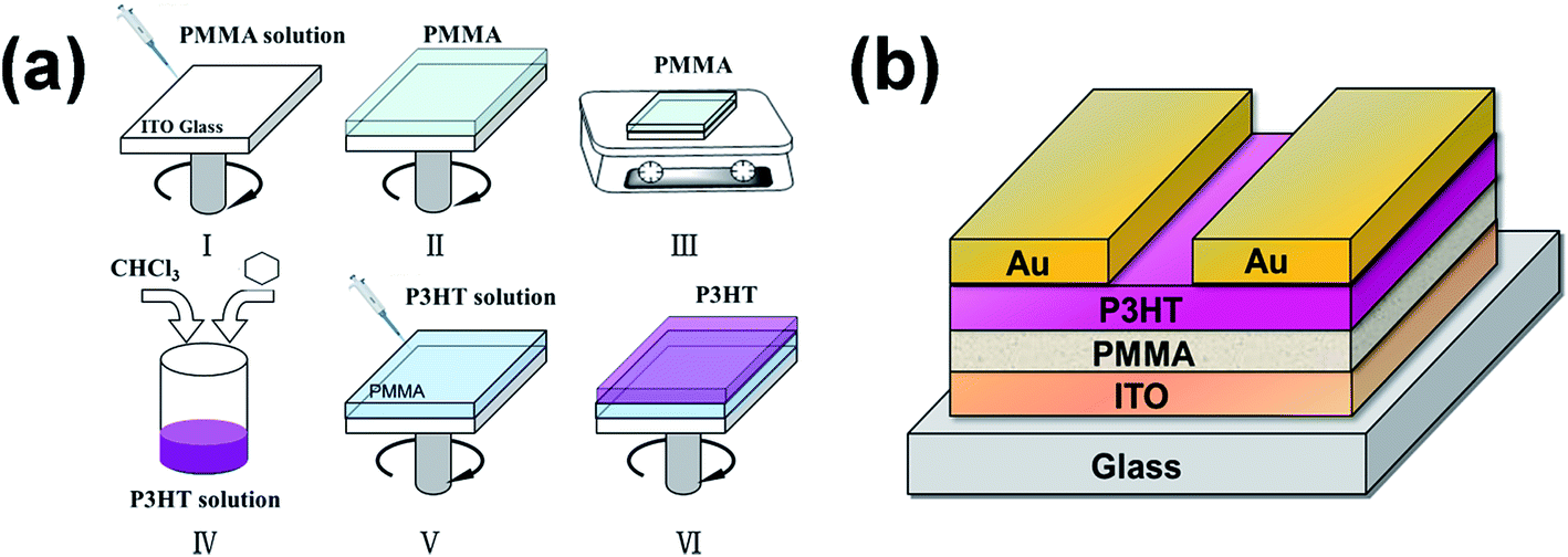 | ||
| Fig. 1 (a) Schematic illustration of the spin-coating process for P3HT/PMMA bilayers; (b) structure of FETs based on P3HT/PMMA bilayers with a BGTC configuration. | ||
Fig. 1(b) shows the BGTC structure of the FET devices based on the P3HT/PMMA bilayers. The devices were constructed on ITO-coated glass substrates with ITO, PMMA, and P3HT acting as the gate electrode, gate dielectric layer, and active layer, respectively. Au films (thickness, 80 nm) were thermally deposited on P3HT with a shadow mask to prepare the source and drain electrodes, defining a channel with a relatively long length of 400 μm and width of 10000 μm. Furthermore, a metal–insulator–metal (MIM) structure was used to study the electrical characteristics of the PMMA films, whose surfaces were treated with mixed cyclohexane/chloroform solvents with volume ratios (Cy:Ch) of 9:1, 8:2, 7:3, and 6:4, respectively. The films were sandwiched between ITO-coated glass and thermally evaporated aluminum (Al) films, which served as negative and positive electrodes, to form an ITO/PMMA/Al structure with an area of 4.5 mm2.
The morphologies of the PMMA films and P3HT/PMMA bilayers were characterized by scanning electron microscopy (SEM), and the surface roughness values of the PMMA films were estimated using atomic force microscopy (AFM). The currents of the PMMA dielectric layers and the output and transfer characteristics of the FET devices were measured with a Keithley 4200 semiconductor analyzer. C–V measurements of the PMMA layers and P3HT/PMMA FET devices were conducted with an Agilent E4990A impedance analyzer. All measurements were performed under ambient conditions.
3. Results and discussion
Morphologies of polymer semiconductor/dielectric bilayers
Determining the mixed solvent ratio that provided the necessary degree of orthogonality to PMMA was of vital importance for creating high-quality polymer bilayers. Firstly, the effect of the solvent ratio on P3HT/PMMA bilayer formation and the P3HT surface morphology was investigated. Fig. 2 shows cross-sectional SEM images of the P3HT/PMMA bilayers. The P3HT films were spin-coated on PMMA from the mixed solvents with Cy:Ch ratios of 9:1, 8:2, 7:3, and 6:4. P3HT/PMMA bilayers were observed to form as the Cy:Ch ratio changed from 9:1 to 6:4, with a clear interface observed at a ratio of 7:3. This was due to no chemical reactions occurring between P3HT and PMMA, as indicated by Fourier transform infrared (FTIR) spectra of the blends of the two polymers,28 and P3HT having a smaller molecular weight. However, a continuous and uniform P3HT film could not be produced on PMMA (not shown) when the Cy:Ch ratio was 5:5 because the larger proportion of chloroform resulted in dissolution and severe damage of the PMMA layer.
 | ||
| Fig. 2 Cross-sectional and top-view (insets) SEM images of P3HT/PMMA bilayers with P3HT layers spun cast from cyclohexane/chloroform mixed solvents at volume ratios of (a) 9:1, (b) 8:2, (c) 7:3, and (d) 6:4. | ||
Cross-sectional SEM images of the bilayers showed that the thickness of the PMMA layer decreased with increasing chloroform concentration in the mixed solvent. The thicknesses of the PMMA layers prepared at Cy:Ch ratios of 9:1, 8:2, 7:3, and 6:4 were estimated to be 420, 400, 380, and 240 nm, respectively. This observation was due to more PMMA being dissolved and re-spin-coated on P3HT, leading to a reduction in PMMA thickness due to a lack of strong interactions between P3HT and PMMA. In contrast, the P3HT layer thickness increased with chloroform content. At a Cy:Ch ratio of 9:1, the P3HT layer was much thinner because it was not completely dissolved in the mixed solvent according to the solubility of P3HT in chloroform.29 As the chloroform ratio was increased to 7:3 (30%), the thickness of P3HT increased to about 100 nm as P3HT became completely soluble.
The insets of Fig. 2 show top-view SEM images of the bilayers. The solvent ratio was also observed to affect the surface morphology of the P3HT film indirectly. A smooth and uniform P3HT surface was observed when the Cy:Ch ratio was varied from 9:1 to 7:3, whereas some clusters were observed at a 6:4 ratio. This might be due to increased interface roughness caused by the dissolution of more PMMA and subsequent redeposition of the dissolved PMMA. This is expected when a thin liquid film is deposited onto a rough solid substrate10 and will be confirmed by AFM characterization.
In FETs with a BGTC configuration, a dielectric surface was extremely important because a rough surface prevents charge transport by acting as a physical trap and transport barrier, or by disturbing the morphology and the microstructures of the semiconducting layer.30,31 To understand the impact of the cyclohexane/chloroform ratio (degree of orthogonality) in the mixed solvent, we characterized the PMMA surface treated with mixed solvent containing no P3HT using AFM measurements. This strategy was feasible because the amount of P3HT in the mixed solution was low and P3HT has no chemical interactions with PMMA. A similar approach8 has been used to examine the effects of solvents for PMMA layers on the surfaces of P3HT and poly ([N,N-9-bis(2-octyldodecyl)-naphthalene-1,4,5,8-bis(dicarboximide)-2,6-diyl]-alt-5,59-(2,29-bithiophene)) (P(NDI2OD-T2)) films in devices with a top-gate architecture.
Fig. 3 shows AFM micrographs of the pristine PMMA film surface and PMMA film surfaces treated with mixed solvent with Cy:Ch ratios of 7:3 and 6:4, and cyclohexane alone. Both PMMA films spun cast from cyclohexane and the mixed solvent with 7:3 ratio exhibited similar surface morphologies to the pristine PMMA film, while the film treated with a 6:4 solvent ratio showed some clusters. The root-mean-square (RMS) roughness values were evaluated as 0.391, 0.458, 0.418, and 14.858 nm, respectively. As expected, the RMS roughness of the PMMA film treated with only cyclohexane (100% Cy) was similar to that of the pristine PMMA film, showing that cyclohexane had no impact on the roughness of PMMA owing to its complete orthogonality to PMMA. The RMS roughness of the PMMA film spun cast from mixed solvent with a 7:3 ratio was comparable with that of the pristine PMMA film, which indicated that the PMMA surface remained almost unaffected, even at chloroform concentrations as high as 30%. Nevertheless, when the chloroform ratio was further increased to 6:4, the PMMA film showed a more coarse surface with a high roughness of 14.858 nm, confirming speculation about the increased interface roughness at a solvent ratio of 6:4. Evidently, only chloroform altered the degree of orthogonality of the mixed solvent and impacted the PMMA surface quality. When the chloroform ratio reached 6:4 (40%), a rougher PMMA surface was produced by the dissolution and redeposition of more PMMA during mixed-solvent treatment. The top-view SEM images in the insets of Fig. 2(c) and (d) and the AFM images in Fig. 3(c) and (d) show a similar trend in the surface morphology of the P3HT/PMMA bilayer and the RMS roughness of the mixed-solvent-treated PMMA surface as the chloroform concentration was increased.
 | ||
| Fig. 3 AFM micrographs (3 μm × 3 μm) of (a) the pristine PMMA film surface and (b) PMMA film surfaces treated with cyclohexane/chloroform mixed solvents with volume ratios of (b) 100% cyclohexane, (c) 7:3, and (d) 6:4. | ||
Therefore, by simply changing the ratio of the orthogonal solvent to the good solvent, namely the degree of orthogonality with respect to PMMA, we were able to control the interface roughness and produce well-controlled P3HT/PMMA bilayers exhibiting solvent corrosion issues. The critical chloroform content in the mixed solvent was found to be 30% (Cy:Ch = 7:3), below which the RMS roughness of the interface was relatively low, at less than 0.500 nm, and the top P3HT layer showed a smooth and uniform surface. We concluded that the optimal ratio of cyclohexane to chloroform in the mixed solvent for producing a high-quality P3HT/PMMA bilayer was 7:3, because the bilayer had a P3HT thickness desirable for FETs, in addition to a clear interface and smooth P3HT surface morphology. Therefore, this mixed-solvent method is not limited to the P3HT/PMMA system, but could also be applied to fabricating other bilayer polymer FETs to overcome solvent corrosion problems encountered in film deposition using a solution-based process.
Electrical properties of polymer dielectric films
The device performance of the polymer FETs was strongly correlated not only with the semiconductor/dielectric interfaces, but also the electrical properties of gate dielectrics. Fig. 4 shows curves of the current density and capacitance per unit area vs. the voltage of the ITO/PMMA/Al devices. The PMMA surfaces were treated with mixed solvents at Cy:Ch ratios of 9:1, 8:2, 7:3, and 6:4. Fig. 4(a) shows that the current densities of the PMMA films treated with solvents with 9:1 and 8:2 ratios were similar at voltages ranging from −50 to 0 V. These values were smaller than the current densities of films treated with the 6:4 mixed solvent, but larger than those of the films treated with 7:3 mixed solvent. The difference in the current density was primarily attributed to the thickness of the PMMA film. The current density increased as the PMMA thickness decreased with increasing chloroform concentration. The current densities for all PMMA films were below 10−8 A cm−2, indicating that they had good insulating properties. The PMMA film treated with a 7:3 solvent ratio possessed the lowest current densities, which guaranteed stable FET operations.
 | ||
| Fig. 4 (a) Current density–voltage and (b) capacitance per unit area-frequency characteristics of PMMA films with surfaces treated with cyclohexane/chloroform mixed solvents at volume ratios of 9:1, 8:2, 7:3, and 6:4. The PMMA films were sandwiched between ITO and Al electrodes. | ||
Fig. 4(b) shows that the capacitance per unit area of all ITO/PMMA/Al devices decreased when the signal frequency was increased from 100 to 106 Hz. This capacitance reduction with increasing frequency was mainly attributed to a reduction in the dielectric constant of PMMA,20 which resulted from dipoles failing to reorient with the electric field in the high-frequency range.32 The capacitance of the PMMA layer was also observed to increase with increasing chloroform concentration. The capacitance of a dielectric film is known to be inversely proportional to its thickness. Obviously, the increase in capacitance resulted from a reduction in the PMMA thickness with increasing chloroform concentration. The capacitance of the PMMA layer treated with a 7:3 solvent ratio at 100 Hz was 3.75 nF cm−2, which was sufficient for electric charge induction. Evidently, the optimal cyclohexane/chloroform mixed solvent ratio for P3HT was 7:3, in which a high-quality P3HT/PMMA bilayer was produced and the treated PMMA layer had a low current density and sufficient capacitance for field-effect conduction.
Electrical performance of polymer bilayer field-effect transistors
We fabricated polymer FETs based on the P3HT/PMMA bilayers using the optimal cyclohexane/chloroform ratio of 7:3, which had an ITO(Gate)/PMMA/P3HT/Au(Source/Drain) structure, as shown in Fig. 1(a). The electrical output and transfer characteristics of the devices are illustrated in Fig. 5. The gate voltage ranged from 0 to −60 V in steps of −10 V as the source-drain voltage was swept from 0 to −60 V. The transfer curves shown in Fig. 5(b) were recorded at a source-drain voltage of −40 V. This device worked through charge accumulation at the P3HT/PMMA interface upon applying a gate voltage and showed a typical p-channel behavior, which consists of linear and saturation regions. The mobility and the threshold voltage can be determined from the transfer characteristics in the saturation regime using eqn (1):
 | (1) |
 | ||
| Fig. 5 (a) Output and (b) transfer characteristics of the P3HT/PMMA bilayer FET prepared using cyclohexane/chloroform mixed solvent at the optimal volume ratio of 7:3. | ||
For comparison, previously reported polymer FETs based on P3HT and PMMA5,9,11,12,21,22,24,33 and our device are summarized in Table 1, indicating structure, fabrication technique, channel length and width, and mobility value. The mobilities of the polymer FETs based on P3HT and PMMA varied over three orders of magnitude, from 10−3 to 10−1 cm2 V−1 s−1, depending on device configurations, fabrication methods, and channel lengths. The mobility has been demonstrated to increase as the channel length is reduced.34 The highest mobility value of 0.2 cm2 V−1 s−1 was achieved in the TGBC devices by spin coating with a channel length of 20 μm.24 The BGTC devices of a 120 μm-long channel constructed by a dry transfer technique11 had a mobility of 1.4 × 10⁻³ cm2 V−1 s−1. Mobilities ranging from 0.001–0.022 cm2 V−1 s−1 were achieved in BGTC devices fabricated by vertical phase separation.12 Therefore, despite a much longer channel length of 400 μm, our FET devices based on P3HT/PMMA bilayers prepared using a cyclohexane–chloroform mixed solvent at the optimal ratio of 7:3 exhibited good device performance.
| Polymer/polymer | Structure | Method | Channel L/W (μm) | Mobility (cm2 V−1 s−1) | References |
|---|---|---|---|---|---|
| PMMA/P3HT | TGBC | Spin coating | 100/17200 |
9.99 × 10⁻³ | 5 |
| PMMA/P3HT | TGBC | Spin coating | 20/1000 | 0.02–0.04 | 9 |
| PMMA/P3HT | TGBC | Spin coating | 20/1000 | 0.08–0.2 | 24 |
| PMMA/P3HT | TGBC | Spin coating | 50/150 | 2.5 × 10⁻³ | 21 |
| PMMA/P3HT | TGBC | Spin coating | 40/5000 | 0.05 | 33 |
| PMMA/P3HT | TGBC | Dry transfer | 30/110 | 0.013 | 22 |
| P3HT/PMMA | BGTC | Dry transfer | 120/3000 | 1.4 × 10⁻³ | 11 |
| P3HT:PMMA |
BGTC | Vertical phase separation | — | 0.001–0.022 | 12 |
| P3HT/PMMA | BGTC | Mixed-solvent method | 400/10000 |
4.4 × 10⁻³ | This work |
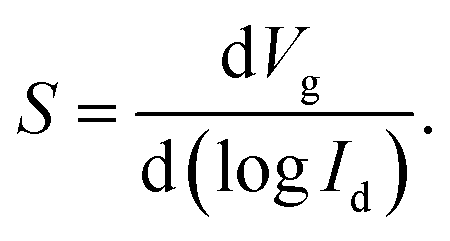
Subthreshold swing S is another important device parameter for quantifying how sharply a transistor can be switched from the off-state to the on-state by a gate voltage.17–19 S is defined as the change in the gate voltage needed to induce a drain-current change of one order of magnitude (eqn (2)):
 | (2) |
Fig. 6(a) shows the same data as Fig. 5(b), but on a logarithmic scale. The red line is a linear fit of the measured data in the voltage region from the off-state to the on-state, from which a subthreshold swing (S) of 14 V per decade (dec) was estimated for the P3HT/PMMA FET device. This value was within the range of the subthreshold swings (1–20 V dec−1) reported for organic and polymer FETs in most published studies.35
 | ||
| Fig. 6 (a) Logarithmic plot of the data shown for P3HT/PMMA FET in Fig. 5(b). (b) Capacitance per unit area–voltage characteristics at a frequency of 500 kHz and normalized capacitance with respect to the maximum capacitance C0 in accumulation at −40 V for the polymer FET based on the P3HT/PMMA bilayer prepared with cyclohexane–chloroform mixed solvent at the optimal volume ratio of 7:3. The voltage was only applied to the ITO gate electrode and one Au electrode. Inset: Mott–Schottky plot of capacitance vs. voltage. | ||
Comparative studies of traps at polymer semiconductor/dielectric interfaces
The quality of the semiconductor/dielectric interface in a polymer FET determines the subthreshold swing.17 With a simplistic assumption that the density of interface traps is independent of energy, the maximum interface trap density is given by eqn (3):
 | (3) |
:3 has a good P3HT/PMMA interface.
Lastly, to further study the properties of the traps at the P3HT/PMMA interface in the FET device, we conducted high-frequency capacitance measurements19 directly on the device with a voltage only applied between the ITO gate electrode and one Au electrode, which apparently constructed an ITO/PMMA/P3HT MIS structure. The area of the MIS capacitor was 0.2 cm−2, defined by the area of the Au electrode. The capacitance of the FET device was measured by sweeping the bias voltage from −40 to +40 V with a small superimposed AC signal of 100 mV at 500 kHz on top of a preselected DC voltage. Fig. 6(b) shows typical curves of capacitance per unit area (C) vs. voltage for the MIS capacitor from its normalized value (C/C0) to the maximum value (C0) at −40 V. These C–V curves were similar to that of an ideal MIS structure.19 Accumulation, transition, and full depletion regions, but no inversion region, were clearly observed as the voltage ranged from −40 to 40 V, which was consistent with the capacitance vs. voltage behavior of polymer MIS structures.20,38 The maximum value of the capacitance per unit area at −40 V was equal to that of the PMMA insulating layer (Ci) because the P3HT semiconducting layer driven into accumulation was in a conducting state.
The difference in work function between ITO (5.1 eV) and P3HT (5.0 eV) was 0.1 eV in the P3HT/PMMA FET device and could be considered negligible.20,38 We evaluated the trap density at the P3HT/PMMA interface according to deviations in the C–V curve from that of an ideal MIS capacitor, if all charges in the dielectric were assumed to be located at the interface. This assumption was reasonable because a greater effect on the C–V behavior was expected if the charges in the dielectric were closer to the interface. In general, charges in the interface traps of polymer MIS capacitors can shift the flat band voltage, which is zero for an ideal MIS capacitor, and deform the C–V curves.20,38 The total capacitance under flat-band conditions19 for an ideal MIS structure can be expressed as follows (eqn (4)):
 | (4) |
Usually, the dopants in a semiconducting polymer are residual or unintentional impurities. The dopant density can be extracted based on the standard Mott–Schottky relation for an MIS capacitor in depletion (eqn (5)):39–41
 | (5) |
The corresponding voltage of this flat band capacitance in Fig. 6(b) was the flat band voltage, VFB, which was about 6 V for the device. The flat band voltage shift in the positive voltage direction indicated negative charges trapped at the P3HT/PMMA interface with acceptor-type interface traps.20,38 Assuming that all charges in the dielectric were located at the interfaces, the density of the interface traps, Nit, responsible for the VFB shift was calculated using eqn (6):20
 | (6) |
Actually, the interface trap density derived from the subthreshold swing was the same as that calculated from the capacitance measurement, but expressed in a different unit. The interface trap density in cm−2 eV−1 characterized the distribution of the interface trap levels across the energy bandgap19 between LUMO and HOMO levels in a polymer semiconductor. Therefore, it was reasonable that the interface trap density of the PMMA/P3HT FET device in cm−2 eV−1 evaluated from the subthreshold swing was larger than that in cm−2 estimated from the C–V measurements.
4. Conclusion
We have proposed a mixed-solvent method for producing high-quality polymer bilayers by spin-coating to solve solvent corrosion issues at the interfaces. This method has been applied to fabricating P3HT/PMMA bilayers. The mixed solvent for P3HT consisted of cyclohexane, an orthogonal solvent of PMMA, and chloroform, a good solvent of P3HT. By changing the ratio of cyclohexane to chloroform, namely the degree of orthogonality with respect to PMMA, we produced well-controlled P3HT/PMMA bilayers. The optimal cyclohexane–chloroform ratio for preparing a high-quality P3HT/PMMA bilayer for field-effect conduction was found to be 7:3. The bilayer under these conditions had a clear interface with low roughness, a smooth P3HT surface morphology, a desirable P3HT thickness, and a PMMA dielectric layer with good electric properties.
We investigated the performance of FET devices based on the optimal P3HT/PMMA bilayers with a BGTC configuration. The device exhibited a comparable hole mobility of 4.4 × 10⁻³ cm2 V−1 s−1 despite a much longer channel length of 400 μm. The subthreshold swing of the device was 14 V dec−1, from which the maximum density of the interface traps was determined to be 3.6 × 1012 cm−2 eV−1, characterizing the distribution of the interface trap levels across the bandgap between the LUMO and HOMO levels in P3HT. The results of C–V measurements on the MIS structure in the device suggested that the traps at the P3HT/PMMA interface were acceptor-type and that the density of the interface traps was 2.3 × 1011 cm−2. Notably, the interface trap density in cm−2 eV−1, evaluated from the subthreshold swing, and that in cm−2, estimated from the C–V measurements, were in good agreement. Our mixed-solvent method is not limited to the P3HT/PMMA system, but could also be applied to fabricating other polymer FETs based on various combinations of polymer semiconductors and dielectrics that show solvent corrosion problems during successive film deposition using a solution-based process.
Conflicts of interest
There are no conflicts to declare.Acknowledgements
This work was supported by the National Natural Science Foundation of China (No. 61675018, 61674012, 61475014, and 61775011).References
- X. Sun, C.-a. Di and Y. Liu, J. Mater. Chem., 2010, 20, 2599 RSC.
- T. G. Bäcklund, H. G. O. Sandberg, R. Österbacka, H. Stubb, T. Mäkelä and S. Jussila, Synth. Met., 2005, 148, 87–91 CrossRef.
- A. B. Rodríguez, M. R. Tomlinson, S. Khodabakhsh, J.-F. Chang, F. Cousin, D. Lott, H. Sirringhaus, W. T. S. Huck, A. M. Higgins and M. Geoghegan, J. Mater. Chem. C, 2013, 1, 7736 RSC.
- Y. Yan, L. B. Huang, Y. Zhou, S. T. Han, L. Zhou, J. Zhuang, Z. X. Xu and V. A. Roy, Sci. Rep., 2015, 5, 15770 CrossRef CAS PubMed.
- L. Zhang, D. Yang, S. Yang and B. Zou, Appl. Phys. A: Mater. Sci. Process., 2014, 116, 1511–1516 CrossRef CAS.
- C. de Col, A. Nawaz, I. Cruz-Cruz, A. Kumar, A. Kumar and I. A. Hümmelgen, Org. Electron., 2015, 17, 22–27 CrossRef CAS.
- K.-J. Baeg, A. Facchetti and Y.-Y. Noh, J. Mater. Chem., 2012, 22, 21138 RSC.
- L. S. Cardoso, J. C. Stefanelo and R. M. Faria, Synth. Met., 2016, 220, 286–291 CrossRef CAS.
- K.-J. Baeg, ETRI J., 2011, 33, 887–896 CrossRef.
- S. S. Chang, A. B. Rodríguez, A. M. Higgins, C. Liu, M. Geoghegan, H. Sirringhaus, F. Cousin, R. M. Dalgleish and Y. Deng, Soft Matter, 2008, 4, 2220 RSC.
- J. Park, S.-O. Shim and H. H. Lee, Appl. Phys. Lett., 2005, 86, 073505 CrossRef.
- X. Wang, W. H. Lee, G. Zhang, X. Wang, B. Kang, H. Lu, L. Qiu and K. Cho, J. Mater. Chem. C, 2013, 1, 3989 RSC.
- K. P. Pernstich, D. Oberhoff, C. Goldmann and B. Batlogg, Appl. Phys. Lett., 2006, 89, 213509 CrossRef.
- H. L. Gomes, P. Stallinga, M. Cölle, D. M. de Leeuw and F. Biscarini, Appl. Phys. Lett., 2006, 88, 082101 CrossRef.
- F.-Y. Yang, K.-J. Chang, M.-Y. Hsu and C.-C. Liu, J. Mater. Chem., 2008, 18, 5927 RSC.
- J. Park, S. Y. Park, S.-O. Shim, H. Kang and H. H. Lee, Appl. Phys. Lett., 2004, 85, 3283–3285 CrossRef CAS.
- W. L. Kalb and B. Batlogg, Phys. Rev. B: Condens. Matter Mater. Phys., 2010, 81, 035327 CrossRef.
- K. N. N. Unni, S. Dabos-Seignon and J.-M. Nunzi, J. Mater. Sci., 2006, 41, 317–322 CrossRef CAS.
- S. M. Sze and k. K. Ng, Physics of Semiconductor Devices, John Wiley & Sons, 2006 Search PubMed.
- M. Estrada, F. Ulloa, M. Avila, J. Sanchez, A. Cerdeira, A. Castro-Carranza, B. Iniguez, L. F. Marsal and J. Pallares, IEEE Trans. Electron Devices, 2013, 60, 2057–2063 CrossRef CAS.
- M. Estrada, I. Mejia, A. Cerdeira and B. Iñiguez, Solid-State Electron., 2008, 52, 53–59 CrossRef CAS.
- I. Mejia, M. Estrada and M. Avila, Microelectron. Reliab., 2008, 48, 1795–1799 CrossRef CAS.
- J. Li, Z. Sun and F. Yan, Adv. Mater., 2012, 24, 88–93 CrossRef CAS PubMed.
- K.-J. Baeg, D. Khim, D.-Y. Kim, J. B. Koo, I.-K. You, W. S. Choi and Y.-Y. Noh, Thin Solid Films, 2010, 518, 4024–4029 CrossRef CAS.
- L. Reséndiz, M. Estrada, A. Cerdeira, B. Iñiguez and M. J. Deen, Org. Electron., 2010, 11, 1920–1927 CrossRef.
- D. Ennis, H. Betz and H. Ade, J. Polym. Sci., Part B: Polym. Phys., 2006, 44, 3234–3244 CrossRef CAS.
- Y. Ma, X. Cao, X. Feng, Y. Ma and H. Zou, Polymer, 2007, 48, 7455–7460 CrossRef CAS.
- M. E. Nicho, C. H. García-Escobar, M. C. Arenas, P. Altuzar-Coello, R. Cruz-Silva and M. Güizado-Rodríguez, Mater. Sci. Eng., B, 2011, 176, 1393–1400 CrossRef CAS.
- F. Machui, S. Langner, X. Zhu, S. Abbott and C. J. Brabec, Sol. Energy Mater. Sol. Cells, 2012, 100, 138–146 CrossRef CAS.
- Y. Don Park, J. A. Lim, H. S. Lee and K. Cho, Mater. Today, 2007, 10, 46–54 CrossRef.
- Z. Bao and J. Locklin, Organic field-effect transistors, CRC Press, Boca Raton, 2007 Search PubMed.
- E. Reis Simas, E. S. H. Kang, A. Gassmann, E. Katholing, S. Janietz and H. von Seggern, J. Mater. Chem. C, 2015, 3, 9217–9223 RSC.
- M. Wang, F. Jakubka, F. Gannott, M. Schweiger and J. Zaumseil, Org. Electron., 2014, 15, 809–817 CrossRef CAS.
- G. Wang, J. Swensen, D. Moses and A. J. Heeger, J. Appl. Phys., 2003, 93, 6137–6141 CrossRef CAS.
- O. Marinov, M. J. Deen and B. Iniguez, IEE P.–Circ. Dev. Syst., 2005, 152, 189 CrossRef.
- D. M. Taylor and N. Alves, J. Appl. Phys., 2008, 103, 054509 CrossRef.
- I. Torres, D. M. Taylor and E. Itoh, Appl. Phys. Lett., 2004, 85, 314–316 CrossRef CAS.
- Y. K. Lee and S. P. Murarka, Mater. Res. Bull., 1999, 34, 869–876 CrossRef CAS.
- E. J. Meijer, A. V. G. Mangnus, C. M. Hart, D. M. de Leeuw and T. M. Klapwijk, Appl. Phys. Lett., 2001, 78, 3902–3904 CrossRef CAS.
- O. Marinov, M. J. Deen, B. Iniguez and B. Ong, J. Vac. Sci. Technol., A, 2006, 24, 649–653 CAS.
- I. Torres and D. M. Taylor, J. Appl. Phys., 2005, 98, 073710 CrossRef.
- D. M. Taylor, J. A. Drysdale, I. Torres and O. Fernández, Appl. Phys. Lett., 2006, 89, 183512 CrossRef.
| This journal is © The Royal Society of Chemistry 2018 |