
 Open Access Article
 This Open Access Article is licensed under a
 Creative Commons Attribution 3.0 Unported Licence
Fabrication of Cu2ZnSn(S,Se)4 photovoltaic devices with 10% efficiency by optimizing the annealing temperature of precursor films†
Pengpeng Zhangab,
Qing Yuab,
Xue Minab,
Linbao Guoab,
Jiangjian Shia,
Xiangyun Zhaoc,
Dongmei Liab,
Yanhong Luoab,
Huijue Wua,
Qingbo Meng *ab and
Sixin Wu*c
*ab and
Sixin Wu*c
aKey Laboratory for Renewable Energy (CAS), Beijing Key Laboratory for New Energy Materials and Devices, Institute of Physics, Chinese Academy of Sciences, Beijing 100190, China. E-mail: qbmeng@iphy.ac.cn
bSchool of Physical Sciences, University of Chinese Academy of Sciences, Beijing 100049, China
cThe Key Laboratory for Special Functional Materials of MOE, Henan University, Kaifeng, Henan 475004, China. E-mail: wusixin@henu.edu.cn
First published on 23rd January 2018
Abstract
The annealing temperature of solution-processed Cu2ZnSn(S,Se)4 (CZTSSe) precursor films has been carefully optimized for favorable selenization. At higher temperature, more solvent will be removed, and the crystallinity of the precursor films can be improved. It is found that, although the crystallinity of selenized film is continuously enhanced by increasing the temperature, a dense CZTSSe film with round and large grains can only be achieved at medium high temperature ranging from 350 to 400 °C. Further investigation reveals that, in this regime, the carrier and defect densities are obviously reduced, leading to average photoelectric conversion efficiency (PCE) improved from 5.1% to 9.4%. An optimal annealing temperature of 380 °C is obtained and up to 10.04% of photoelectric conversion efficiency has been achieved.
1. Introduction
Kesterite Cu2ZnSn(S,Se)4 (CZTSSe) photovoltaics have received considerable attention in recent years as a promising alternative to traditional chalcogenide-based solar cells (e.g., CdTe and Cu(In,Ga)(S,Se)2) because of its non-toxic and earth-abundant constituents.1–4 To fabricate high-efficiency CZTSSe thin film solar cells, a variety of vacuum-based and solution-based deposition methods have been reported for CZTSSe absorber layers.1–6 So far, a certified-record photoelectric conversion efficiency (PCE) of 12.6% has been achieved for CZTSSe solar cells based on a hydrazine-based solution method.4 Compared to vacuum-based deposition methods, solution-based methods have some attractive advantages, such as low-cost process and facile controlling material components, which are thus considered as compelling alternatives to vacuum thin film deposition techniques.Hydrazine is a highly explosive and toxic solvent, which restricts its wide application. Therefore, some low-toxic solvents have been adopted for fabricating CZTSSe films, such as dimethyl sulfoxide (DMSO),5,6 1,3-dimethyl-2-imidazolidinone (DMI)7 and 2-methoxyethanol.8–10 Besides, in order to stabilize the CZTSSe precursor system, some organic ligands (i.e. thioglycolic acid) are also introduced to coordinate to Cu/Zn/Sn atoms. However, these solvents cannot be easily removed by a simple evaporation process, leading to high carbon residues in the absorber film and affecting the semiconductor properties.11–15 Whether these carbon residues in precursor films have negative role on the final device performance or not is still controversial.16–19 Some studies showed that the carbon-rich layer could be completely removed in CZTS precursor film through a lengthy sulfuration.20 Wu et al. obtained a CZTSSe thin film without fine-grain layer through this process before selenization.21 On the other hand, Williams et al. demonstrated that the proper amount of carbon in precursor film is necessary for grain growth even by doping the polystyrene.14 Currently, optimization toward the carbon remained in CZTSSe films is expected to be an effective approach to enhance the device performance.11,12 The high-temperature selenization process could remove some carbon, however, the relatively short selenization process and complicated reactions make this carbon-removing process uncontrollable. The pre-annealing process of the CZTSSe precursor film is the first step to remove the solvents, however, systematic investigation toward this treatment process is still lacking but of great significance.
Here, we adopt low-toxic mixed solvents consisting of 1,2-ethanedithiol and 1,2-ethylenediamine to deposit CZTSSe thin films. The annealing temperature of the CZTSSe precursor film has been systematically investigated to control the carbon removal. We find that the carbon residue in the precursor film can be continuously reduced by increasing the annealing temperature from 300 to 450 °C, which helps to enhance the crystallinities of CZTSSe precursor films and subsequent selenized CZTSSe films. It is revealed that only in the temperature range from 350 to 400 °C, a dense and high quality CZTSSe film can be achieved. Furthermore, the carrier and defect densities are obviously reduced. By controlling precursor film annealing temperatures, the average photoelectric conversion efficiency (PCE) of CZTSSe thin film solar cells has been improved from 5.1% to 9.4% and the champion cell exhibits the 10.04% PCE under the optimal temperature (380 °C).
2. Experimental
2.1 Materials
Cu (99.99%), Zn (99.99%), S powders (99.95%, Aladdin), 1,2-ethylenediamine (AR), 1,2-ethanedithiol (AR), cadmium sulfate (AR) and thiourea (AR) were purchased from Aladdin, Sn (99.8%) and Se powders (99.5%) were from Alfa Aesar, and ammonium hydroxide (AR) was from Sinopharm Chemical Reagent Co. Ltd. All the chemicals were directly used as received without further purification. Mo-sputtered soda lime glass (SLG) substrates were bought from Jinan Lister Electronic Equipment Department.2.2 Preparation of CZTSSe precursor solution
CZTSSe precursor solution was prepared by following previous work.22 Cu (1.65 mmol), Zn (1.23 mmol), Sn (0.98 mmol), S (4 mmol) and Se (0.4 mmol) were loaded into a 10 mL glass vial. Then, 5 mL 1,2-ethylenediamine and 0.5 mL 1,2-ethanedithiol were added into the glass vial. The mixture was continuously stirred for 1.5 h at 90 °C to afford a clear solution.2.3 Fabrication of CZTSSe thin film solar cells
CZTSSe thin film solar cells with a configuration of SLG/Mo/CZTSSe/CdS/ZnO/ITO/Ag were fabricated. The fabrication process of CZTSSe precursor films was carried out in the nitrogen-filled glove box. The CZTSSe precursor solution was spin-coated at 5000 rpm for 30 s on a 2 × 2 cm2 Mo-sputtered soda lime glass (SLG) substrate, followed by annealing on a precise temperature-controlled hotplate. The same process was repeated five times to give about 1.5 μm-thickness precursor films. As-prepared CZTSSe precursor films were selenized under Se atmosphere at 550 °C for 15 min. Subsequently, about 50 nm thickness CdS thin films were deposited on CZTSSe absorber layers by chemical bath deposition (CBD) method, and i-ZnO and ITO thin films were successively deposited by RF-sputtering. Finally, Ag collection grid electrodes were deposited on the top of the ITO film by thermal evaporation under the vacuum of 10−7 torr, giving an active area of 0.18 cm2 for each cell.2.4 Characterization
The thickness of the precursor film was measured by a surface profiler (KLA-Tencor, P-6). The morphologies of the films and the elemental ratios in the precursor film were obtained by scanning electron microscopy (SEM) equipped with energy X-ray dispersive spectroscopy (EDX) on a Hitachi S4800. X-Ray Diffraction (XRD) patterns were measured on a Bruker X-ray diffractometer using Cu Kα as the radiation source. For current–voltage (I–V) measurements, the cells were illuminated under AM 1.5 simulated sunlight (100 mW cm−2) from Zolix SS150A, and I–V curves were recorded on a digital source meter (Keithley model 2602). External quantum efficiency (EQE) of the cells was measured with a lab-made setup under 0.3–0.9 mW cm−2 monochromic light illumination without bias illumination. The capacitance–voltage (C–V) and drive level capacitance profile (DLCP) were carried out on AMETEK Versa STAT 3. C–V plots were obtained at different DC bias voltages ranging from 0.5 to −1.0 V with a perturbation AC voltage of 50 mV at 100 kHz. The DLCP characteristics was measured at different DC bias from 0.5 to −1.0 V with a perturbation AC voltage from 20 to 140 mV at 100 kHz.233. Results and discussion
Fig. 1(a) presents thermogravimetric analysis (TGA) results of CZTSSe precursor films, which were pre-treated at 125 °C for 30 min to remove some solvents in the glove-box. We can see that, the mass loss continuously occurs while increasing the temperature from the room temperature to 700 °C, implying that the organics in the CZTSSe precursor film can hardly be completely removed. As the nucleation and growth behaviors of CZTSSe films in the selenization process are sensitive to the organic remains,17 the annealing temperature for the precursor film needs to be optimized. In terms of previous work about the related solution systems22,24 and unsafety over 450 °C carried out in the glove box, the annealing temperature range of the precursor film is preliminarily selected from 300 to 450 °C. This thermal treatment step is carried out on a hot plate which temperature can be precisely controlled. The mass of samples is found to decrease from 2.4 to 1.8 mg by about 25% mass loss, in good agreement with TGA results (see Fig. 1(b)), in the meantime, the precursor film thickness decreases from 1.6 to 1.3 μm.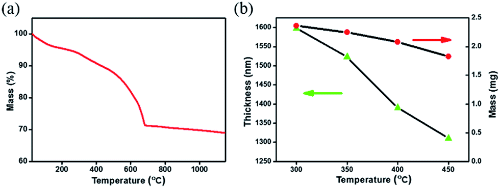 | ||
| Fig. 1 (a) TGA traces of the solid precursors obtained by pre-drying CZTSSe solutions in 1,2-ethylenediamine/1,2-ethanedithiol at 125 °C; (b) changes of mass and thickness of precursor film with respect of changing the processing temperature of precursor films. | ||
Furthermore, atomic ratios of the CZTSSe precursor film annealed at different temperatures were obtained from EDX measurement.3,16,25 For clarity, the amounts of different elements are normalized to that of the Cu, which is stable at high temperature,26 as shown in Fig. 2. For Zn, Sn and Se elements, no obvious change in their atomic ratios is observed at different annealing temperatures. For the S element, the atomic ratio decreases from 2.7 to 2.3 by about 15%, whereas the amount of the carbon element decreases by about 36%. It is thus suggested that, the mass loss mainly comes from organics being removed when increasing the annealing temperature.
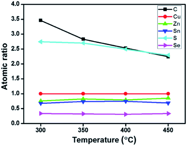 | ||
| Fig. 2 Changes of atomic ratios (other elements/copper) in thermally treated CZTSSe precursor films with respect to different annealing temperatures. | ||
The influence of different annealing temperatures on morphologies and crystallinity of CZTSSe precursor films is also investigated. As shown in Fig. 3(a)–(e), more and larger cracks with random distribution22 can be seen when increasing the temperature, which could be originated from the crystallization induced stress release.27 And a much clearer SEM image is obtained for higher-temperature treated samples, indicating that removing excess organics could improve the film conductivity.12 Besides, XRD patterns of thermally treated CZTSSe precursor films also show better crystallinity while increasing the temperature, mainly due to less organics in the film, as shown in Fig. 3(f).
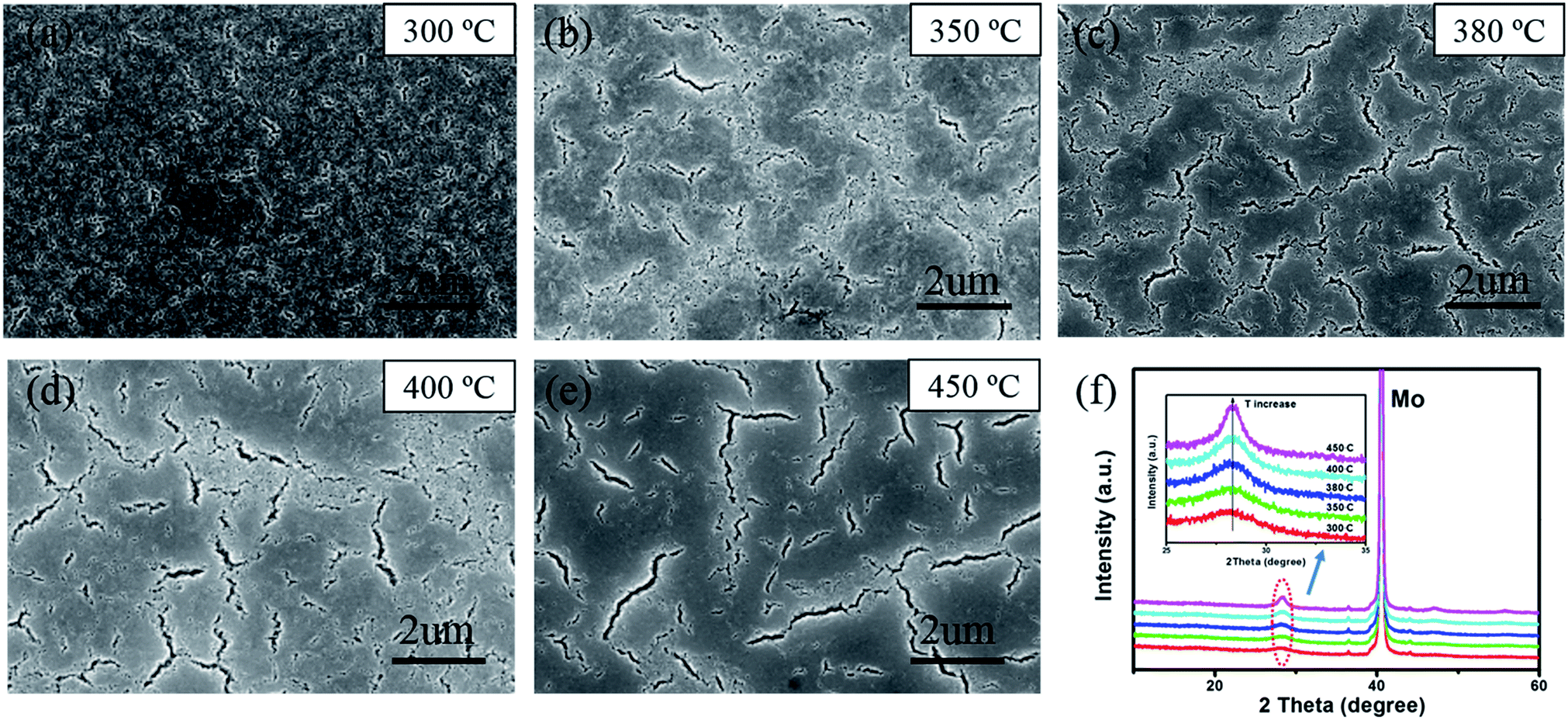 | ||
| Fig. 3 Top-view SEM images of CZTSSe precursor films treated at different annealing temperatures: (a) 300 °C, (b) 350 °C, (c) 380 °C, (d) 400 °C and (e) 450 °C; (f) XRD patterns and enlarged figures of as-prepared CZTSSe precursor films treated at different annealing temperatures. | ||
All the films were further selenized under the same selenization condition (550 °C for 15 min), which was borrowed from the previous work.22 The reduction in organics and crystallinity improvement of precursor films are found to have a significant influence on the morphologies of corresponding selenized films, as shown in Fig. 4(a)–(e). Besides, after selenization, no large cracks of precursor films are found, suggesting that high-temperature selenization process is not only CZTSSe crystal growth and ripening process, but also is able to restructure the film morphology due to the mass transformation and chemical reaction. CZTSSe thin films pre-treated at 300 °C shows the largest grains with obvious voids on the surface. For the films pre-treated at higher annealing temperatures, very little voids are observed but the grain sizes decrease a little at the same time. Films derived from 350 to 400 °C exhibit similar surface morphologies with closely packed grains. For the 450 °C sample, however, a quite different crystal shape with sharp edges is observed. For the 380 °C sample shown in Fig. 4(c), the grains with an average size of about 800 nm are closely and smoothly packed to each other. A cross-sectional SEM image of 380 °C sample in Fig. 4(f) further shows that the CZTSSe film has a bilayer structure as the most works reported.9,22 Below the 800 nm-thick large grains, there is a fine crystal layer with a thickness of about 900 nm. The crystallinity of the selenized films are further explored by grazing XRD. The substrate Mo-peak just disappears when incidence angle omega is 1°. We employ grazing XRD patterns with incidence angle omega = 1° to study the whole absorber layer and grazing XRD patterns with incidence angle omega = 0.1° to study the upper grains. As shown in Fig. 5(a) and (b), there is no obvious intensity change of the main (112) peak of different treated samples when incidence angle omega is 1°. However, XRD patterns with incidence angle omega = 0.1° reveal that the diffraction intensity of the surface crystals is obviously enhanced with the pre-annealing temperature increased, implying the crystallinity improved. The influence on the film crystallinity is mainly assigned to the CZTSSe nucleation and growth processes.17,28 Due to the existence of more organics, the nucleation of CZTSSe crystals is limited, thus yielding less crystal nucleus, larger grains and voids.13,14,27 On the other hand, the mass transport during the crystal growth is also suppressed by these organics, thus affecting the crystallization quality of the surface crystals. By reducing the organics residue, both nucleation rate and mass transport are enhanced, leading to better crystallinity but smaller grains. For the 450 °C sample, the crystals can even grow freely, leading to the appearance of sharp edges and worse grain connection.28
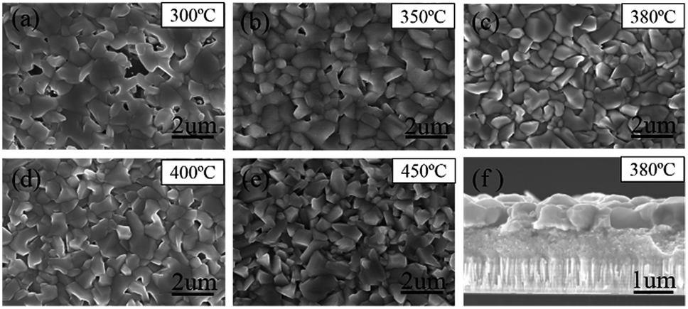 | ||
| Fig. 4 Top-view SEM images of selenized CZTSSe films pre-treated at different annealing temperatures: (a) 300 °C, (b) 350 °C, (c) 380 °C, (d) 400 °C and (e) 450 °C; (f) cross-sectional SEM image of as-selenized CZTSSe thin film annealed at 380 °C. | ||
 | ||
| Fig. 5 XRD patterns with grazing incidence angle (a) omega = 1° and (b) omega = 0.1° for selenized CZTSSe thin films pre-treated at different annealing temperatures. | ||
Based on these CZTSSe films, the complete solar cell with a structure of Mo/CZTSSe/CdS/ZnO/ITO/Ag was fabricated. To get more relationship between the pre-annealing temperature of precursor films and the device performance, the performance characteristics are statistically summarized from 30 solar cells and shown as box-charts in Table 1 and Fig. 6(a)–(d). Detailed photovoltaic performance parameters of each device are listed in Table S1.† Also, the stability of solar cells stored in the ambient condition is measured and the result is shown in Fig. S1.† No obvious performance degradation is found within the two weeks. Obviously, the average PCE is improved from 5.1% to 9.4% when the pre-annealing temperature of precursor film increased from 300 to 380 °C, then decreases to 7.4% when further increasing the pre-annealing temperature to 450 °C. For 300 °C-treated samples, a large distribution in the performance characteristics is found, indicating its low repeatability. This repeatability is significantly enhanced for higher temperatures. The Voc and PCE exhibit the similar dependence on the pre-annealing temperature for precursor film. It is thus suggested that optimal pre-treating temperature is 380 °C. Furthermore, the statistic PCE distribution of 30 cells based on 380 °C-treated sample, is shown in Fig. 6(e). Fig. 6(f) gives the I–V curves of the best performed cell under AM 1.5 illumination and in the dark, respectively, which has a short-circuit current density (Jsc) of 33.5 mA cm−2, an open-circuit voltage (Voc) of 481 mV, a fill factor (FF) of 0.623, giving the best PCE of 10.04%. And the EQE of the champion CZTSSe solar cell is also shown in Fig. S2.† As we know that the carrier and defect densities of selenized CZTSSe absorber have a deeply influence on the Voc and PCE,4,23 it is expected that the changes in Voc and PCE may derive the different carrier and defect densities of the selenized CZTSSe film.
| Annealing temperature | PCE (%) | WD (nm) | NC–V (cm−3) | NDLCP (cm−3) | ΔN |
|---|---|---|---|---|---|
| 300 °C | 5.1 | 114 | 3.62 × 10¹⁶ | 1.67 × 10¹⁶ | 1.95 × 10¹⁶ |
| 350 °C | 8.8 | 184 | 1.09 × 10¹⁶ | 6.34 × 10¹⁵ | 4.56 × 10¹⁵ |
| 380 °C | 9.4 | 201 | 9.44 × 10¹⁵ | 6.61 × 10¹⁵ | 2.83 × 10¹⁵ |
| 400 °C | 8.5 | 142 | 2.46 × 10¹⁶ | 1.23 × 10¹⁶ | 1.23 × 10¹⁶ |
| 450 °C | 7.4 | 122 | 4.67 × 10¹⁶ | 2.41 × 10¹⁶ | 2.26 × 10¹⁶ |
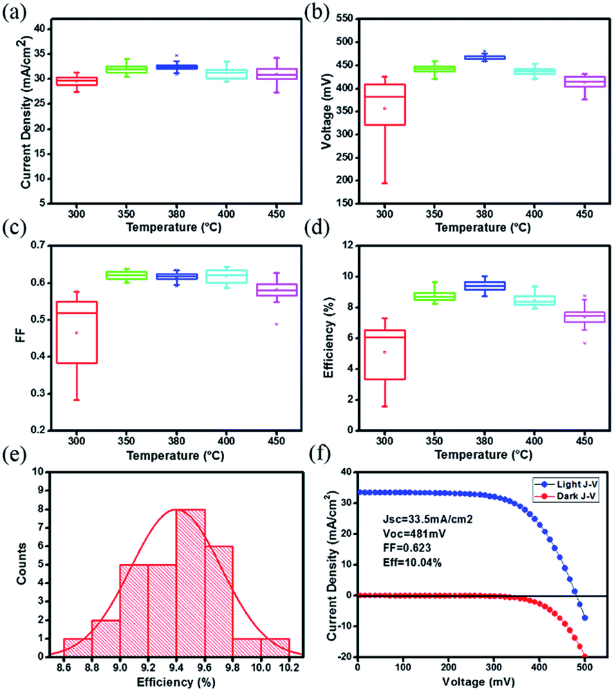 | ||
| Fig. 6 Statistical box charts of photovoltaic parameters of 30 cells based on CZTSSe films pre-treated at different annealing temperatures: (a) short-circuit photocurrent density, (b) open-circuit voltage, (c) fill factor, (d) efficiency; (e) the histogram of PCEs of 30 solar cells; (f) J–V characteristics of the champion CZTSSe solar cell. | ||
To confirm this hypothesis, the charge density and heterojunction depletion width (WD) of the devices based on CZTSSe precursor films at different annealing temperatures were obtained by the C–V and DLCP, respectively.4,23 As shown in Fig. 7, the carrier and defect densities of the CZTSSe film have been significantly influenced by annealing temperatures. The 300 °C treated sample has a high hole density of 3.62 × 1016 cm−3 and a small WD = εA/C of 114 nm, where ε = 8 is dielectric constant, A is the total cell area, and C is capacitance at 0 V bias. By gradually increasing the temperature to 380 °C, the hole density significantly decreases to about 9.44 × 1015 cm−3 and a higher WD of about 200 nm is obtained. This increase in the WD is expected to benefit for the photocarrier extraction and transport.23 However, when further increasing the temperature, the WD is reduced instead, which is in accordance with the decrease in the cell efficiency. Besides, the defect density of the film surface region is also estimated from the difference between the charge density of C–V and DLCP measurement, as shown in Table 1. The 380 °C-treated sample gives the smallest surface defect density, in good agreement with the cell performance.
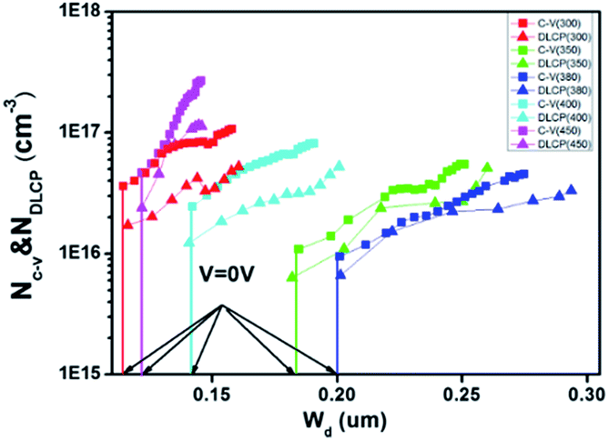 | ||
| Fig. 7 C–V and DLCP characteristics of the CZTSSe solar cells based on the precursor films at different annealing temperatures. | ||
4. Conclusion
Annealing temperatures of CZTSSe precursor films have been optimized for further selenization. It is found that a higher annealing temperature toward precursor films is beneficial to remove organics residues. And the crystallinity of the selenized CZTSSe films can also be effectively improved. However, excessively high pre-annealing temperature would lead to sharp-edges of CZTSSe crystals and worse grain connection of the CZTSSe film. Only at the temperatures ranging from 350 to 400 °C, selenized CZTSSe films with dense and rounded surface morphology can be obtained. Optimal annealing temperature is obtained at 380 °C. Furthermore, the carrier and surface defect densities of selenized CZTSSe absorbers are also significantly suppressed by adjusting annealing temperatures, leading to the average PCE improved from 5.1% to 9.4%. The champion cell with PCE of 10.04% has been achieved under the optimal annealing temperature.Conflicts of interest
There are no conflicts to declare.Acknowledgements
This work is supported by Natural Science Foundation of China (No. 91733301, 51627803, 51402348, 51372272, 51421002 and 51372270) and the Knowledge Innovation Program of the Chinese Academy of Sciences.Notes and references
- J. J. Scragg, T. Ericson, X. Fontané, V. Izquierdo-Roca, A. Pérez-Rodríguez, T. Kubart, M. Edoff and C. Platzer-Björkman, Prog. Photovolt: Res. Appl., 2014, 22, 10–17 CrossRef CAS
.
- K. Wang, B. Shin, K. B. Reuter, T. Todorov, D. B. Mitzi and S. Guha, Appl. Phys. Lett., 2011, 98, 051912 CrossRef
- B.-A. Schubert, B. Marsen, S. Cinque, T. Unold, R. Klenk, S. Schorr and H.-W. Schock, Prog. Photovolt: Res. Appl., 2011, 19, 93–96 CrossRef CAS
- W. Wang, M. T. Winkler, O. Gunawan, T. Gokmen, T. K. Todorov, Y. Zhu and D. B. Mitzi, Adv. Energy Mater., 2014, 4, 1301465 CrossRef
- S. G. Haass, M. Diethelm, M. Werner, B. Bissig, Y. E. Romanyuk and A. N. Tiwari, Adv. Energy Mater., 2015, 5, 1500712 CrossRef
- H. Xin, J. K. Katahara, I. L. Braly and H. W. Hillhouse, Adv. Energy Mater., 2014, 4, 1301823 CrossRef
- V. Tunuguntla, W.-C. Chen, P.-H. Shih, I. Shown, Y.-R. Lin, J.-S. Hwang, C.-H. Lee, L.-C. Chen and K.-H. Chen, J. Mater. Chem. A, 2015, 3, 15324–15330 CAS
- Z. Su, K. Sun, Z. Han, H. Cui, F. Liu, Y. Lai, J. Li, X. Hao, Y. Liu and M. A. Green, J. Mater. Chem. A, 2014, 2, 500–509 CAS
- Q. Tian, G. Wang, W. Zhao, Y. Chen, Y. Yang, L. Huang and D. Pan, Chem. Mater., 2014, 26, 3098–3103 CrossRef CAS
- X. Min, J. Shi, L. Guo, Q. Yu, P. Zhang, Q. Tian, D. Li, Y. Luo, H. Wu, Q. Meng and S. Wu, Chin. Phys. B, 2017, 27, 016402 Search PubMed
- V. T. Tiong, Y. Zhang, J. Bell and H. Wang, RSC Adv., 2015, 5, 20178–20185 RSC
- T. J. Huang, X. Yin, C. Tang, G. Qi and H. Gong, ChemSusChem, 2016, 9, 1032–1041 CrossRef CAS PubMed
- B. D. Chernomordik, A. E. Béland, D. D. Deng, L. F. Francis and E. S. Aydil, Chem. Mater., 2014, 26, 3191–3201 CrossRef CAS
- B. A. Williams, M. A. Smeaton, N. D. Trejo, L. F. Francis and E. S. Aydil, Chem. Mater., 2017, 29, 1676–1683 CrossRef CAS
- T. R. Martin, J. K. Katahara, C. N. Bucherl, B. W. Krueger, H. W. Hillhouse and C. K. Luscombe, Chem. Mater., 2015, 28, 135–145 CrossRef
- X. Lin, J. Kavalakkatt, A. Ennaoui and M. C. Lux-Steiner, Sol. Energy Mater. Sol. Cells, 2015, 132, 221–229 CrossRef CAS
- R. Mainz, B. C. Walker, S. S. Schmidt, O. Zander, A. Weber, H. Rodriguez-Alvarez, J. Just, M. Klaus, R. Agrawal and T. Unold, Phys. Chem. Chem. Phys., 2013, 15, 18281–18289 RSC
- K. E. Roelofs, Q. Guo, S. Subramoney and J. V. Caspar, J. Mater. Chem. A, 2014, 2, 13464–13470 CAS
- W. Wu, Y. Cao, J. V. Caspar, Q. Guo, L. K. Johnson, I. Malajovich, H. D. Rosenfeld and K. R. Choudhury, J. Mater. Chem. C, 2014, 2, 3777–3781 RSC
- B. A. Williams, A. Mahajan, M. A. Smeaton, C. S. Holgate, E. S. Aydil and L. F. Francis, ACS Appl. Mater. Interfaces, 2015, 7, 11526–11535 CAS
- S.-H. Wu, C.-W. Chang, H.-J. Chen, C.-F. Shih, Y.-Y. Wang, C.-C. Li and S.-W. Chan, Prog. Photovolt: Res. Appl., 2017, 25, 58–66 CrossRef CAS
- J. Guo, Y. Pei, Z. Zhou, W. Zhou, D. Kou and S. Wu, Nanoscale Res. Lett., 2015, 10, 1045 Search PubMed
- J. Li, H. Wang, M. Luo, J. Tang, C. Chen, W. Liu, F. Liu, Y. Sun, J. Han and Y. Zhang, Sol. Energy Mater. Sol. Cells, 2016, 149, 242–249 CrossRef CAS
- D. H. Webber and R. L. Brutchey, J. Am. Chem. Soc., 2013, 135, 15722–15725 CrossRef CAS PubMed
- L. Sun, J. He, H. Kong, F. Yue, P. Yang and J. Chu, Sol. Energy Mater. Sol. Cells, 2011, 95, 2907–2913 CrossRef CAS
- N. J. Carter, R. Mainz, B. C. Walker, C. J. Hages, J. Just, M. Klaus, S. S. Schmidt, A. Weber, W.-C. D. Yang, O. Zander, E. A. Stach, T. Unold and R. Agrawal, J. Mater. Chem. C, 2015, 3, 7128–7134 RSC
- R. M. German, P. Suri and S. J. Park, J. Mater. Sci., 2008, 44, 1–39 CrossRef
- C. J. Hages, M. J. Koeper, C. K. Miskin, K. W. Brew and R. Agrawal, Chem. Mater., 2016, 28, 7703–7714 CrossRef CAS
Footnote |
| † Electronic supplementary information (ESI) available. See DOI: 10.1039/c7ra13069d |
| This journal is © The Royal Society of Chemistry 2018 |