
 Open Access Article
 This Open Access Article is licensed under a Creative Commons Attribution-Non Commercial 3.0 Unported Licence
Fabrication of a cobalt phthalocyanine free-standing film on an ionic liquid surface for memory device applications
Yan Xiaoab,
Long Zhanga,
Fei Penga and
Ge-Bo Pan *a
*a
aSuzhou Institute of Nano-Tech and Nano-Bionics, Chinese Academy of Sciences, 215123 Suzhou, P. R. China. E-mail: gbpan2008@sinano.ac.cn
bUniversity of Chinese Academy of Sciences, 100049 Beijing, P. R. China
First published on 31st January 2018
Abstract
The fabrication of a metal phthalocyanine (MPc) film with good transferability and exploitation of its properties are very important for further application. In this study, a continuous free-standing film of CoPc was obtained on an ionic liquid (IL) surface via a physical vapor deposition (PVD) method. The as-obtained film has a β-phase structure and is constructed with one dimensional CoPc to form a network structure. The morphology of the film could be easily tuned by tunning the flow rate of the carrier gas. More importantly, the device based on these films shows obvious electrical switching and negative differential resistance (NDR) characteristics. The maximum ON/OFF current ratio of two distinctive conductivity states is ∼100 at a reading voltage of +30 V. The conductivity and conductive switching behavior of the NW constructed device are better than the device constructed with NRs. The NDR effect and electrical switching conduction mechanism can be explained by the charge trap elements of the CoII/CoI redox couples. The above results open up the possibility of CoPc as a memory medium for information storage and logic circuits applications.
1 Introduction
Organic thin films constructed with a one-dimensional (1D) nanostructure are currently under intense investigation. They can provide efficient charge generation and transport in one direction owing to their unique structural as well as physical properties1 and have potential applications in nanoscale electronic, optical, and optoelectronic devices.2–7 Compared with their inorganic counterparts, organic materials open up a bright vista for the next generation of nanotechnologies and electronic devices8 because organic materials have many advantages which include unlimited choices of building blocks, versatile modification of materials on the molecular level, high flexibility, low cost, and ease of large-area fabrication. Moreover, among various building blocks for organic nanostructured films, organic small conjugated molecules have been extensively studied for their good crystallinity and high mobility. Metal phthalocyanines (MPcs) are one of the most widely studied organic functional materials because their planar aromatic structures are ideal building blocks for organic nanostructures through π–π interactions and the possibility of applications in various opto/electronic devices including photovoltaics, rectifiers, memory devices, organic photodetectors, sensors etc.9–12CoPc is a member of MPcs family with the central atom as Co2+ and an 18 π-electron system. The presence of the superoxide adduct of CoPc leads to the formation of charge-transfer complexes and then induce the formation injection of hole charge carriers into the bulk solid.13 Such phenomena induces good conductivity and catalytic of CoPc. Despite the electronic applications of CoPc, e.g. organic field-effect transistors,14 gas sensor15 and electrocatalysts16 have been widely studied, the exploitation of CoPc in a wider application is still very important. On the other hand, the preparation of CoPc films with various micro/nano structures is mainly focused on physical vapor deposition (PVD) due to its low solubility. The significant obstacle in such process is that the films are generally difficult to lift off and transfer because of the strong material–substrate interaction, which limited further device application. Free-standing film, which can overcome such obstacle and can be easily transferred onto the desired substrate for further devices application to decrease remarkably the cost without sacrificing the device performance was discovered in recent years.17
In this study, a free-standing film of CoPc was successfully prepared via PVD method and its memory switching property was observed for the first time. In particularly, considering the unique physical and chemical properties of ionic liquid (IL) such as zero pressure of saturated vapor, extended temperature range, good chemical and thermal stability and low flammability,18–20 we have also introduced ILs as substrate into PVD system for CoPc deposition. After deposition, a continuous CoPc film was obtained on the surface of 1-(2-hydroxyethyl)-3-methylimidazolium tetrafluoroborate ([HEMIM][BF4]). The film is constructed with one dimensional (1D) network structure and the morphology can be easily tuned by modulating the flow rate of carrier gas. More importantly, the device which based on these films shows obvious electrical switching and negative differential resistance (NDR) characteristics. Our results demonstrate that CoPc is a promising organic semiconductor as memory medium for the applications of information storage and logic circuits.
2 Experimental section
Synthesis and characterization
Synthesis of the CoPc (Aldrich co.) free-standing film was conducted in a horizontal quartz tube furnace using ILs as the growth substrate via a PVD method. In a typical procedure, 5 mg CoPc powder was placed at the high temperature zone of the furnace. The tested IL was [HEMIM][BF4] (Shanghai Chengjie Chemical Co., Ltd), which has higher density than CoPc and was insoluble with CoPc. 3 ml ILs were loaded in a quartz boat and placed at downstream positions ∼16 cm from the source material. After the tube was evacuated to a base pressure of 2 Pa, a carrier gas (nitrogen, 99.999%) was fed with a constant flow ratio and the pressure in the tube was adjusted to 220 Pa during the experiments. Thereafter, the source material was heated to 550 °C at and then maintained at this temperature for 60 min. Finally, the final products were detached from the ILs by immersing in water, whereupon the ILs were dissolved. Besides the flow rate of nitrogen mainly affected the morphology of the final products, and flow rate of carrier gas between 100 sccm and 200 sccm were investigated.The fabricated samples were examined by scanning electron microscopy (SEM, Quanta 400 FEG), transmission electron microscope (TEM, Tecnai G2 F20 S-Twin), energy-dispersive X-ray spectrometry (EDS, Quanta 400 FEG), X-ray diffraction (XRD, X‘Pert-Pro MPD), Fourier-transform infrared spectroscopy (FT-IR, Nicolet 6700), UV-vis-NIR absorption spectra (UV-vis, Lambda 750), cyclic voltammetry measurement (CV, CHI 660D Shanghai ChenHua Co., Ltd).
Memory device fabrication and measurements
The memory device was constructed in bottom-connected configuration. The finger electrodes with the length of 200 μm, the width of 20 μm and the distance of 20 μm, were fabricated by the photolithography and electron beam deposition of Au on the SiO2/Si substrate. The devices were fabricated on the basises of as-obtained CoPc films. In brief, CoPc film was rinsed with methanol to remove the residual ILs and then transferred onto the as-fabricated Au electrode of SiO2/Si substrate. Current–voltage (I–V) characteristics of the devices were recorded with a Keithley 4200 SCS and SUSS PM8 probe station in a clean and shielded box at room temperature. All measurements were carried out at room temperature under ambient conditions.3 Results and discussion
After deposition, a blue layer of CoPc film was observed on the ILs' surface. The thickness of the film depends on the location of ILs and the deposition time. Fig. 1a shows the typical morphology of the as-fabricated film on ILs surface. It was seen that a nanowire (NW) network was formed. The NWs have average width of ∼150 nm, thickness of ∼30 nm and average lengths up to ∼50 μm, which indicates beneficial properties such as large surface-to-volume ratio morphology. As reported, a number of NWs standing on the solid substrate when using solid substrate,14,21 our two dimensional (2D) network structure film may be attribute to the high surface energy (Es) of IL. Fig. 1b displays a typical SEM image of CoPc NWs. It is clear that the NWs exhibit smooth surfaces and uniform diameter. The high magnification SEM image of the NW (see the inset in Fig. 1b) indicated that some of the NW with helical structure. The width, length, and pitch distance of helical nanowires are in the ranges of ∼150 nm, ∼1–5 μm, and ∼300 nm, respectively. Although many helical structures of CoPc have been reported, most of them were based on the twisted nanoribbons,21 the as-prepared helical CoPc NWs in our study are mostly double-stranded or multi-stranded and with same helix direction, which is due to the high viscosity of IL and facilitates CoPc molecules to move in one direction. Representative TEM image of the double-stranded helical structure CoPc NW is shown in Fig. 1c. It shows that the NW has a solid state and further indicates of a smooth surface. High-resolution TEM (HRTEM) of the CoPc NW discloses the single-crystalline nature of the helical NW and with the same growth direction. The CoPc NW grows along [100] direction, and the corresponding d100 is ∼1.53 nm. Furthermore, the area of films could be easily adjusted by varying the size of quartz boat and the quantity of starting materials.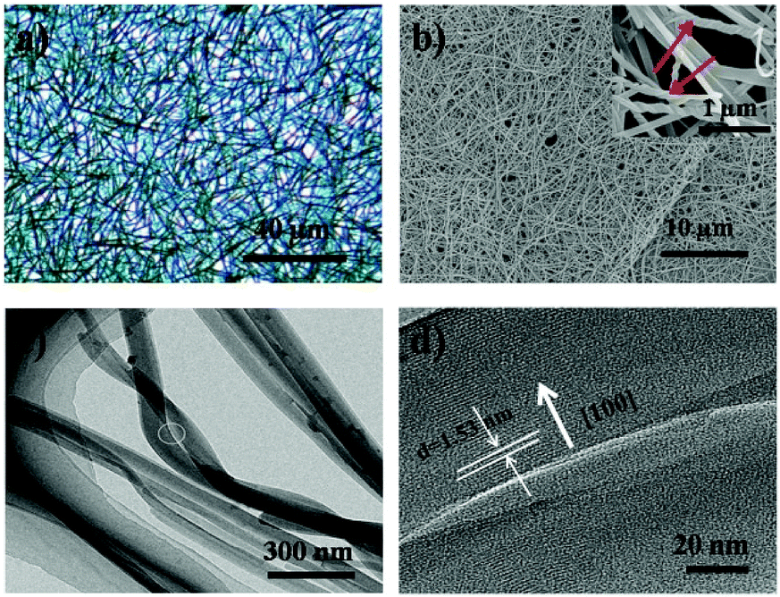 | ||
| Fig. 1 (a) The optical microscopic (OM) image of the as-prepared film on ILs surface. (b) Typical SEM image of CoPc film and inset was the high magnification of the corresponding film. (c) The typical TEM image of the twisted CoPc wire. (d) HRTEM image of the white-marked area in (c). | ||
XRD, FT-IR, UV-vis absorption and EDX spectra have been characterized, in order to understand the chemical composition and the structure of CoPc film. Fig. 2a shows the XRD pattern of CoPc free-standing film and compared with CoPc powder. The XRD pattern of CoPc powder can be indexed as the monoclinic crystal with lattice constants of a = 14.5982 Å, b = 4.7937 Å, c = 19.4348 Å and β = 121.782°, which indicates that the CoPc power was β phase.22 Similar to the XRD pattern of CoPc powder, two diffraction peaks at 7.17° and 9.34° appeared, which were identified as the (100) and (10−2) peaks of β-CoPc. This result revealed that no phase transformation occurred during the vapor deposition process and the highly crystalline with a preferential orientation of (100) of the obtained film. The FT-IR spectrum (Fig. 2b) of CoPc film and CoPc powder in the range 500–1000 cm−1 were tested to reveal the possible structure and chemical composition change of such film. The main peak at 730 cm−1 is assigned to nonplanar deformation of C–H bonds of benzene rings.23 The medium band at 756 cm−1 and a band at 780 cm−1 are ascribed to non-planar vibrations (out-of-plane bending) of the C–H bonds.24 The metal ligand (Co–N) vibration bands are corresponding to 915 and 877 cm−1. As reported, the band of 730, 780 and 877 cm−1 are for the characteristic of β-form CoPc.25 The FT-IR results are in good agreement with the XRD analysis and CoPc did not decomposition or other chemical reactions occurred during the PVD process. Fig. 3c shows the UV-vis spectra of film which transferred onto quartz substrate. The film has three characteristic adsorption bands, labelled as B, Q1, and Q2. In the near-UV region in the range of about 300–350 nm (B-band) exhibits a single peak, representing the π–π* transition between bonding and anti bonding molecular orbital. The absorption band in the visible region known as the Q-band representing the π → π* transition has a doublet due to vibronic coupling in the excited state (Davydov splitting).26 The result indicates that CoPc film with well-defined intermolecular interactions. In addition, Fig. 2d shows the EDS analysis of CoPc films, the elements of C, N, and Co elements that constitute the molecules of CoPc were clearly identified, but no B and F elements exist, indicating no ILs absorbed on the products and the high-purity nature of the final products.
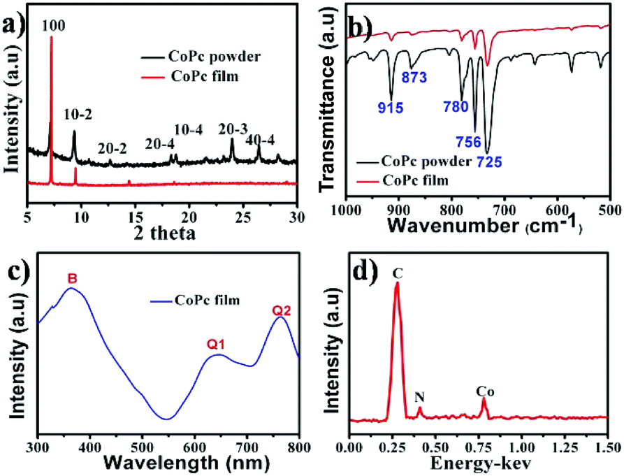 | ||
| Fig. 2 (a) XRD pattern and (b) FT-IR spectra of CoPc film along with CoPc powder; (c) UV-vis and (d) EDS spectra of CoPc film. The CoPc film was obtained on [HEMIM][BF4] surface. | ||
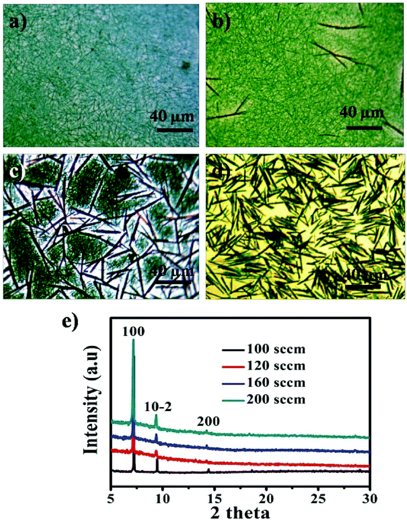 | ||
| Fig. 3 (a–d) Typical OM images and (e) XRD pattern of CoPc nanostructures deposited on ILs surface through heated to 550 °C for 1 h with different flow rate of nitrogen: (a) 100 sccm, (b) 120 sccm, (c) 160 sccm and (d) 200 sccm. | ||
The flow rate of carrier gas (N2) plays an important role in the morphology and crystal phase of CoPc. Fig. 3 shows a set of typical OM images and XRD patterns of the products obtained with different flow rate of nitrogen, while the other parameters were fixed. A NWs network was formed at the flow rate of 100 sccm (Fig. 3a). Some rod like CoPc emerged when the flow rate increased to 120 sccm (Fig. 3b). The content of nanorod (NR) in the blend increases as the flow rate increases (Fig. 3c). Further increasing the flow rate to 200 sccm, the CoPc NRs with diameters of ∼900 ± 100 nm, height of 400 ± 100 nm, and the lengths of 40 ± 10 μm were obtained (Fig. 3d). The significant difference between the NR and NW are the diameters and the height of final products. It indicates that the morphology of the film is closely related with the flow rate of N2. The higher flow rate of N2 induces higher deposition temperature and higher supersaturation of vapor. Consequently, the corresponding high supersaturation vapor combines with high molecule mobility could benefit the π⋯π conjugation between the layer-stacked molecules in different CoPc unit cells and the large size of NR are formed.21 The XRD spectra of the CoPc films obtained with different flow rate of N2 are shown in Fig. 3e. The peak was observed at 2θ = 7.17, 9.34, and 14.4°, which corresponds to the monoclinic CoPc in the (100), (10–2) and (200) plane respectively. The position of the diffraction peak is not changed as changes the flow rate of N2, which confirms that both NWs and NRs have the same β-form crystalline structure.
The impact of the type of IL on the final products was also studied. A continuous free standing film could be obtained only on the surface of [HEMIM][BF4], while suspended CoPc was obtained in the bulk phase of other alkyl imidazolium ILs. Because [HEMIM][BF4] has the highest density among other alkyl imidazolium ILs. The higher density of IL is responsible for CoPc float on the ILs surface, while the high Es contributes to 2D network structure. Because organic molecules could preferentially deposite on the higher Es sites.27
The good transferability of such film made it possible to be easily transferred onto desired substrates for further device application. Fig. 4a is a schematic of a NW network-based device. Fig. 4b shows a typical SEM image of the as-constructed device. It is clear that the NW network has been connected to two Au electrodes. The thickness of the network film is approximately 150 nm. The I–V characteristics of the device exhibit a reversible hysteretic switching and memory behavior. As the sweep from −50 to 50 V, the current remains in the high conducting (ON) state, but during the final bias scan from 50 to −50 V, the low-conducting (OFF) state is retained exhibiting memory phenomena, indicating the bistable properties of the device. At a proper reading voltage (e.g., 30 V), the ON current is 120 nA while the OFF current is only 14 nA giving an ON/OFF ratio of 100. As we know, most of MPc memory devices were prepared with sandwich structure, the ON/OFF ratio in our system is relatively low due to large distance between two electrodes which would not facilitate charge transfer. It is still large enough for detecting in different states. Furthermore, the current initially high, and increases with bias voltage, when the bias voltage reaches a certain value (40 V), the current starts decrease with bias form a negative differential resistance (NDR) region during the sweep from −50 to 50 V. The obvious conductivity switching behavior and NDR characteristics make it potentially useful in nonvolatile rewritable organic bistable memory devices.
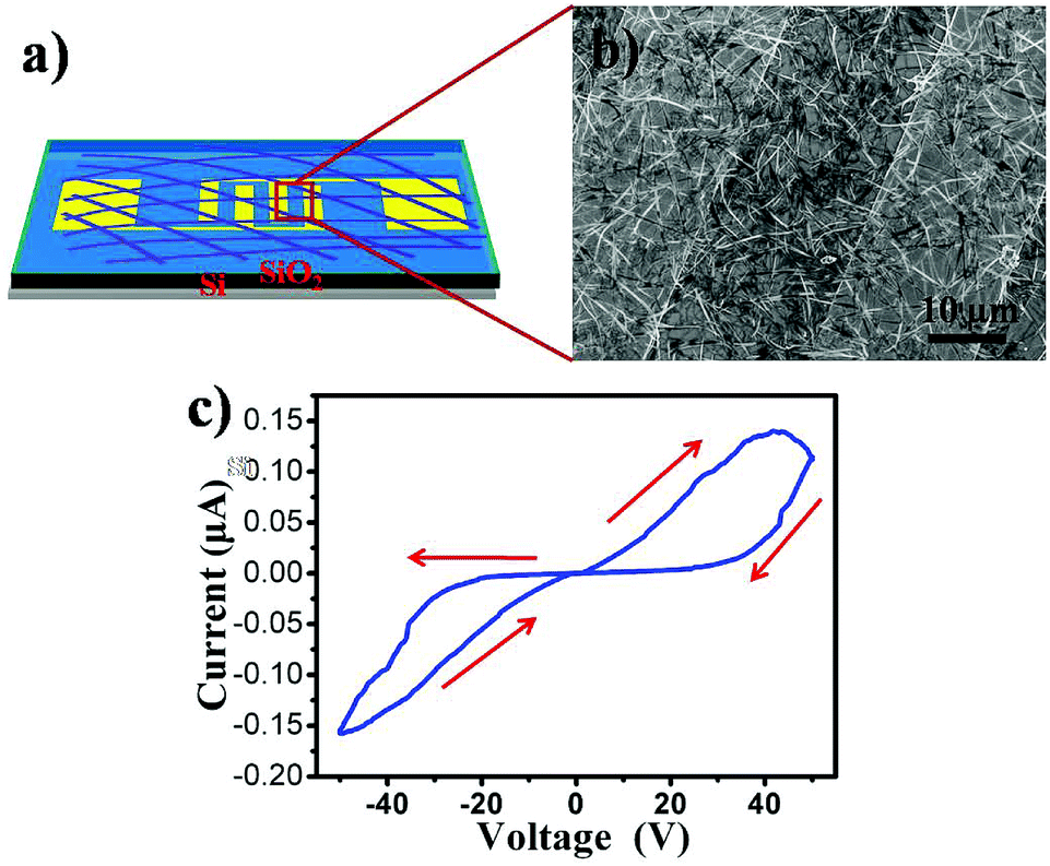 | ||
| Fig. 4 (a) Schematic illustration and (b) representative SEM image of a device based on a CoPc nanowire network film. (c) I–V characteristics of the device for CoPc film. | ||
To study the role of morphology of the CoPc film on electrical bistability of the device, we have compared I–V characteristics of the two devices (Fig. 5). We find that the current values for device I are smaller than for devices II. At a bias voltage of 50 V, the current of ON state was 0.01 μA for device I and 0.032 μA for device II. This is an increase in current by about three magnitude. Furthermore, both device exist conductivity switching behavior and NDR characteristics. A comparison between the results also indicates that the switching is similar for both the devices during the bias scan from 0 to 150 V, while the device II is about 2 magnitude higher than device I during the bias scan from −150 to 0 V. In addition, the NR constructed and the NWs network constructed films were found to have a thickness of ∼800 nm and ∼150 nm, respectively. The large surface-to-volume ratio and slightly thinner thickness of the NWs network film lead to better contact with Au electrode and result in higher conductivity in the device II. As a result, the switching behavior of our devices are strongly depend on the morphology of the active layer.
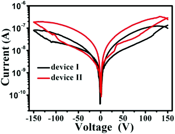 | ||
| Fig. 5 I–V characteristics of the device for two different morphology of the active layer; the active layer of device I was CoPc NR constructed film while the device II was CoPc NWs network constructed film. | ||
The electrochemical activities of CoPc film adsorbed onto ITO electrode was investigated by using cyclic voltammogram (CV), to explain the switching characteristics. Fig. 6 shows CV of PBS at ITO and CoPc/ITO electrode. Compared with ITO electrode, the redox peak −0.71 V was observed at CoPc/ITO (Fig. 6a and b). The redox reactions was attributed to the CoII/CoI of CoPc.28 As shown in Fig. 6c and d, the cathodic and anodic peak currents for the CoPc are linearly proportional to the scan rate, indicating that the electrochemical response is governed by a charge transfer mechanism.29 The bipolar switching behavior in this system can be explained by charge storage (high resistance) and release (low resistance) within charge-trap sites, since these redox reactions have close relationship with electron release (oxidation) and trapping (reduction). In the CoPc film devices, the charge trap element of CoII/CoI redox couples can significantly affect the switching mechanisms of devices.
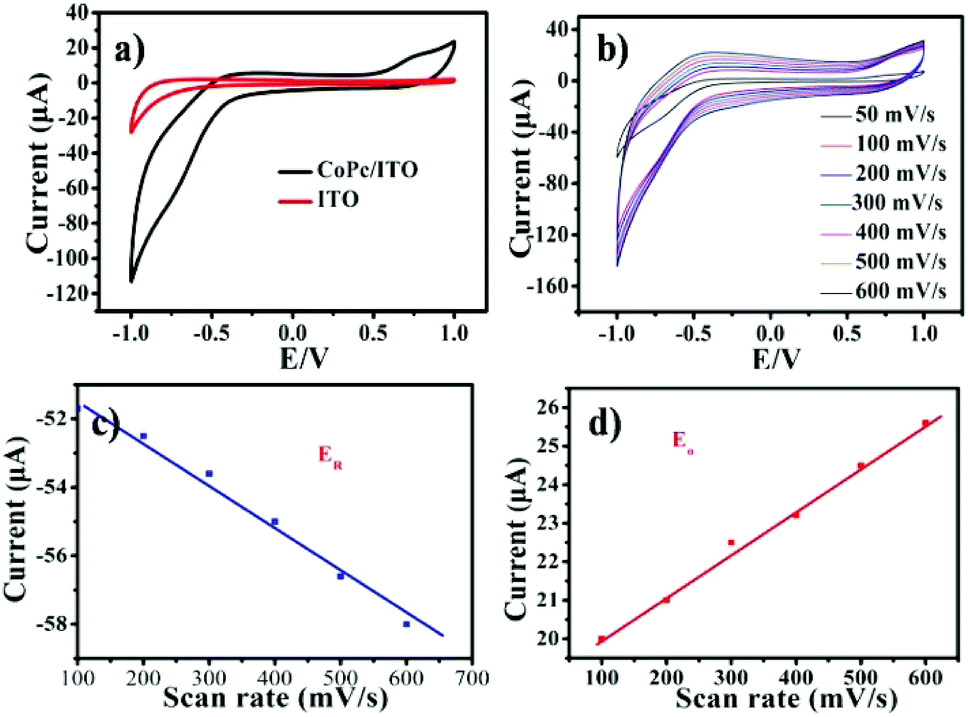 | ||
| Fig. 6 (a) Cyclic voltammogram of bare ITO electrode and CoPc/ITO modified electrode in 0.1 mol L−1 PBS (pH = 7.0), scan rate 100 mV s−1. (b) Cyclic voltammogram of CoPc/ITO electrode in 0.1 mol L−1 PBS (pH = 7.0) at different scan rate. Scan rate dependence of (c) anodic (ER) and (d) cathodic (EO) peak currents. | ||
For further understanding of the mechanism of resistive switching behavior, I–V characteristics are also re-plotted in a log–log scale as shown in Fig. 7. It is found that the ON/OFF current ratio for the NWs based device is larger than for the NRs based device, as shown in Fig. 7a and b. The relations for all devices have the rather similar gradient. The I–V relationship in the ON state clearly exhibits ohmic conductance behavior with a slope of ∼1.3, which indicates the in the device during the “SET” (switch the device from high resistance state to low resistance state) process, however, the conduction behavior of the films in the OFF state is more complicated. The conduction mechanism is in good agreement with the space charge limited conduction (SCLC),30 which consists of three portions: the ohmic region (I ∝ V), Mott–Gurney law (I ∝ V2) and a steep current increase region. The different conduction behaviors in the ON and OFF states imply that conduction behavior of CoPc memory devices is consistent with SCLC and localized filament mechanisms.
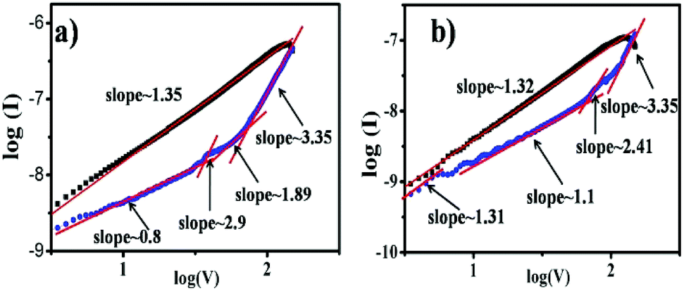 | ||
| Fig. 7 Comparisons of electrical bistability of two device with different deposition morphology of CoPc layer (a) NWs and (b) NRs in log–log scale. | ||
4 Conclusions
We have successfully fabricated a free-standing film of CoPc on ILs surface via a PVD method. The film has β-phase structure and is constructed with 1D CoPc to form network structure. The morphology of the film can be easily controlled just by varying the flow rate of carrier gas. Moreover, the device of such free-standing film exhibited two distinctive states of conductivity with the maximum ON/OFF current ratio ∼100 at reading voltage of +30 V and NDR characteristics. The conductive switching behavior of the NWs constructed device is about 2 magnitude higher than the device constructed with NRs during the bias scan from −150 to 0 V. The conduction mechanism can be ascribed to the charge trap elements of CoII/CoI redox couples, which is consistent with SCLC and localized filament mechanisms. Our results open up the possibility of CoPc as memory medium for the applications of information storage and logic circuits.Conflicts of interest
There are no conflicts to declare.Acknowledgements
This work was financially supported by the National Natural Science Foundation of China (No. 21303250 and 61404155), the National High Technology Research and Development Program of China (No. 2015AA034601), the Jiangsu Province Outstanding Youth Foundation (No. BK20160058), and the Chinese Academy of Sciences.Notes and references
- K. Min, S. B. Jo, J. H. Park and K. Cho, Nano Energy, 2015, 18, 97–108 CrossRef.
- Y. Guo, H. Zhao, G. Yu, C. a. Di, W. Liu, S. Jiang, S. Yan, C. Wang, H. Zhang and X. Sun, Adv. Mater., 2008, 20, 4835–4839 CrossRef CAS.
- J.-S. Hu, H.-X. Ji and L.-J. Wan, J. Phys. Chem. C, 2009, 113, 16259–16265 CAS.
- W. Y. Lee, H. C. Wu, C. Lu, B. D. Naab, W. C. Chen and Z. N. Bao, Adv. Mater., 2017, 29, 7 Search PubMed.
- J. Xu, S. H. Wang, G. J. N. Wang, C. X. Zhu, S. C. Luo, L. H. Jin, X. D. Gu, S. C. Chen, V. R. Feig, J. W. F. To, S. Rondeau-Gagne, J. Park, B. C. Schroeder, C. Lu, J. Y. Oh, Y. M. Wang, Y. H. Kim, H. Yan, R. Sinclair, D. S. Zhou, G. Xue, B. Murmann, C. Linder, W. Cai, J. B. H. Tok, J. W. Chung and Z. N. Bao, Science, 2017, 355, 59–64 CrossRef CAS PubMed.
- J. Ye, C. Zhang, C. L. Zou, Y. Yan, J. Gu, Y. S. Zhao and J. Yao, Adv. Mater., 2014, 26, 620–624 CrossRef CAS PubMed.
- F. X. Wang, J. Lin, W. B. Gu, Y. Q. Liu, H. D. Wu and G. B. Pan, Chem. Commun., 2013, 49, 2433–2435 RSC.
- J. R. Eskelsen, Y. Qi, S. Schneider-Pollack, S. Schmitt, K. W. Hipps and U. Mazur, Nanoscale, 2014, 6, 316–327 RSC.
- J. C. Obirai and T. Nyokong, J. Electroanal. Chem., 2007, 600, 251–256 CrossRef CAS.
- J. Lin and D. Ma, Org. Electron., 2009, 10, 275–279 CrossRef CAS.
- R. Saini, A. Mahajan, R. K. Bedi, D. K. Aswal and K. Debnath, Sens. Actuators, B, 2014, 198, 164–172 CrossRef CAS.
- Q. Tang, H. Li, M. He, W. Hu, C. Liu, K. Chen, C. Wang, Y. Liu and D. Zhu, Adv. Mater., 2010, 18, 65–68 CrossRef.
- F. I. Bohrer, A. Sharoni, C. Colesniuc, J. Park, I. K. Schuller, A. C. Kummel and W. C. Trogler, J. Am. Chem. Soc., 2007, 129, 5640–5646 CrossRef CAS PubMed.
- F. X. Wang, G. H. Yuan, Y. D. Liu and G. B. Pan, Mater. Lett., 2012, 83, 56–58 CrossRef CAS.
- A. Kumar, S. Samanta, S. Latha, A. Debnath, A. Singh, K. Muthe and H. C. Barshilia, RSC Adv., 2017, 7, 4135–4143 RSC.
- H. Yin, Y. Zhou, J. Xu, S. Ai, L. Cui and L. Zhu, Acta Cienc. Indica, Chem., 2010, 659, 144–150 CrossRef CAS PubMed.
- J. Yin, Y. Zhou, T. Lei and J. Pei, Angew. Chem., Int. Ed., 2011, 50, 6320–6323 CrossRef CAS PubMed.
- T. Welton, Chem. Rev., 1999, 99, 2071–2083 CrossRef CAS PubMed.
- P. Wasserscheid, Nature, 2006, 439, 797 CrossRef CAS PubMed.
- L. Meli and T. P. Lodge, Macromolecules, 2009, 42, 580–583 CrossRef CAS.
- W. Tong, A. Djurišić, M. Xie, A. Ng, K. Cheung, W. Chan, Y. Leung, H. Lin and S. Gwo, J. Phys. Chem. B, 2006, 110, 17406–17413 CrossRef CAS PubMed.
- P. Ballirano, R. Caminiti, C. Ercolani, A. Maras and M. A. Orru, J. Am. Chem. Soc., 1998, 120, 12798–12807 CrossRef CAS.
- A. N. Sidorov, Opt. Spectrosc., 1976, 40, 492–499 CAS.
- G. N. Meshkova, A. T. Vartanyan and A. N. Sidorov, Opt. Spectrosc., 1977, 43, 262–266 CAS.
- M. M. El-Nahass, K. F. Abd-El-Rahman and A. A. A. Darwish, Mater. Chem. Phys., 2005, 92, 185–189 CrossRef CAS.
- Y. Zhu, L. Qian, M. Xue, Q. Sheng, Q. Zhang and Y. Liu, Appl. Surf. Sci., 2011, 257, 2625–2632 CrossRef CAS.
- Y.-S. Zhao, P. Zhan, J. Kim, C. Sun and J. Huang, ACS Nano, 2010, 4, 1630–1636 CrossRef CAS PubMed.
- N. Pereira, Bioelectrochemistry, 2007, 70, 147–154 CrossRef PubMed.
- W. S. Alencar, F. N. Crespilho, M. Santos, V. Zucolotto, O. N. Oliveira and W. C. Silva, J. Phys. Chem. C, 2007, 111, 12817–12821 CAS.
- B. Koo, H. Baek and J. Cho, Chem. Mater., 2012, 24, 1091–1099 CrossRef CAS.
| This journal is © The Royal Society of Chemistry 2018 |