
 Open Access Article
 This Open Access Article is licensed under a Creative Commons Attribution-Non Commercial 3.0 Unported Licence
A study of the density of states of ZnCoO:H from resistivity measurements†
Miyeon Cheon a,
Yong Chob,
Chul-Hong Parkc,
Chae Ryong Chod and
Se-Young Jeong*ef
a,
Yong Chob,
Chul-Hong Parkc,
Chae Ryong Chod and
Se-Young Jeong*ef
aCrystal Bank Research Institute, Pusan National University, Miryang 50463, Korea
bKorea Research Institute of Standards and Science, Daejeon 34113, Korea
cDept. of Physics Education, Pusan National University, Busan, 46241, Korea
dDepartment of Nanoenergy Engineering, College of Nanoscience and Nanotechnology, Pusan National University, Busan 46241, Republic of Korea
eDept. of Cogno-Mechatronics Engineering, Pusan National University, Busan, 46241, Korea. E-mail: cpark@pusan.ac.kr; syjeong@pusan.ac.kr; Fax: +82-55-353-1314; Tel: +82-55-350-5273
fDept. of Optics and Mechatronics Engineering, Pusan National University, Miryang, 50463, Korea
First published on 8th March 2018
Abstract
Understanding the electronic band structure and density of states (DOS) of a material and their relationship to the associated electronic transport properties is the starting point for optimizing the performance of a device and its technological applications. In a hydrogenated Zn0.8Co0.2O (ZnCoO:H) film with an inverted thin-film transistor structure, we found ambipolar behavior, which is shown in many field-effect devices based on graphene, graphene nanoribbons, and organic semiconductors. In this study, to obtain information on the DOS of ZnCoO:H to explain the ambipolar behavior in terms of the carrier density and type, resistivity and magnetoresistance measurements of a ZnCoO:H film were performed at 5 K. Our proposed DOS representation of ZnCoO:H explains qualitatively the experimental observations of carrier density modulation and ambipolar behavior. First-principles calculations of the DOS of ZnCoO:H were in good agreement with the proposed DOS representation. Through a comparison of first-principles calculations and experimental data, evidence for the existence of Co–H–Co in ZnCoO:H is suggested.
Introduction
Chemical doping is commonly used to modify the electronic properties of a material.1,2 However, it can be difficult to synthesize a variety of samples with precisely controlled doping ratios. Doped elements inherently induce disorder that may, in turn, increase resistivity. Alternatively, application of an external voltage creates an electric field that varies the carrier density in the material; thus, in this manner, the resistance can be changed without inducing disorder. Field-effect transistors (FETs) are typically used for this purpose. An applied voltage induces electron flow between the source and drain electrodes; the electron flow is controlled by the gate. In practice, an insulating layer (SiO2, Si3N4, etc.) is deposited on a heavily doped semiconducting substrate with the gate electrode (back-gate) beneath. Applying a gate voltage creates a change in the electric field across the insulating layer, resulting in modulation of the surface charge density of the insulating layer, similar to capacitor behavior. By modifying the carrier density in the insulating layer, the insulating layer acts as a second parallel plate of a capacitor and therefore tunes its Fermi energy level. Significant carrier accumulation/depletion has led to various achievements in condensed matter physics, such as metal–insulator transitions in ZnO 3 and an ambipolar field effect in graphene.4–7The ambipolar field effect has been observed in graphene-based FETs; the unique cone-like zero gap band structure of this material produces a V-shaped transfer characteristic curve.4,5 In neutral graphene, the Fermi level is positioned at the Dirac point, which generates zero density of states (DOS). The Dirac point separates the region of conduction via electrons from that of holes. In addition to graphene, a wide variety of semiconducting materials (e.g., from conventional silicon to recently studied nanoribbon graphene, reduced graphene oxide, single-walled carbon nanotubes, quantum dots, and two-dimensional materials) exhibit ambipolar characteristics.8–12 Recently, ambipolar behavior has also been demonstrated in solution-deposited ZnO/pentacene bilayer transistors and hydrogen-incorporated ZnO nanowires.13,14 ZnO has been used extensively in thin-film transistor (TFT) applications, such as transparent displays, due to its excellent properties, including a wide direct band gap of 3.4 eV at room temperature, a large exciton binding energy of 60 meV, high electron mobility and high thermal conductivity, as well as nontoxicity. Also, as one of the most promising spin device materials, ZnCoO and ZnCoO:H have attracted much attention due to room temperature ferromagnetism, as reported by several groups15–17 even though there is still some debate about the origin, reproducibility and consistency of room temperature ferromagnetism in these systems. Some experimental18,19 and theoretical20–23 studies of the role of hydrogens in ZnCoO have shown that the origin of ferromagnetism in ZnCoO:H might be Co–H–Co complexes mediated by unintentionally doped hydrogens. The macroscopic percolation of Co–H–Co complexes would result in ferromagnetic long-range ordering. In our previous studies, we demonstrated this controllable ferromagnetism by controlling the amount of doped hydrogen atoms24 and observed the relation between the electrical properties and hydrogenation.25 In this study, we doped a small concentration of hydrogen atoms into ZnCoO to prevent Co–H–Co complexes from percolating, to study the electrical properties through a rise in conductivity due to hydrogenation without long range magnetic ordering.
Here, we provide a comprehensive representation of the relationship between resistivity and DOS in ZnCoO:H by manipulating the carrier density and carrier type. The simple proposed DOS of ZnCoO:H explains qualitatively the experimental observations of carrier density modulation in ZnCoO:H, as well as the behavior of the resistivity. First-principles calculations provided confirmation that the proposed DOS representation was reasonable.
Materials and methods
Sample fabrications
Using radio frequency sputtering, a cobalt (20 mol%)-doped ZnO film (thickness: 100 nm) was deposited on a p-type Si substrate covered with a 100 nm-thick insulating layer of Si3N4 (provided by Crystal Bank-NRF2015M3A9B8047340 Pusan National University, Korea). To change the carrier concentration, a TFT structure was adapted using a p-doped Si substrate and Si3N4 layer as the bottom electrode and insulating layer, respectively. During the sputtering process, the substrate temperature was maintained at 300 °C in a high purity (99.99%) argon atmosphere. For transport measurements, a Hall bar with a 1 mm × 10 mm channel was fabricated using conventional ultraviolet (UV)-lithography and etched in an NH4Cl aqueous solution. After defining the Hall bar, the sample was plasma-treated for 1 min in an Ar![[thin space (1/6-em)]](https://www.rsc.org/images/entities/char_2009.gif) :H2 (80:20 wt%) gas mixture at RT to inject hydrogen into the surface of the film (ZnCoO:H); details are provided in a previous study.25
:H2 (80:20 wt%) gas mixture at RT to inject hydrogen into the surface of the film (ZnCoO:H); details are provided in a previous study.25
Resistivity measurements
The magnetotransport properties of the sample at 5 K were measured using a Physical Properties Measurement System (PPMS-9; Quantum Design), two source meters (Keithley 2425C, 2635A), a nanovoltmeter (Keithley 2182A), and a switcher (Keithley 7001). During the measurements, the gate voltage was swept between −20 V and 20 V, with a fixed magnetic field. The magnetic field was perpendicular to both the sample surface and the direction of the current. The longitudinal voltage, Vxx, and Hall voltage, Vxy, were averaged as the direction of current was changed for each gate voltage. The longitudinal resistivity ρxx (conductivity σxx) is defined as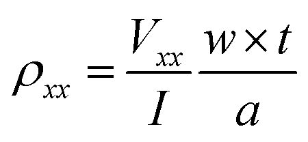 , (
, (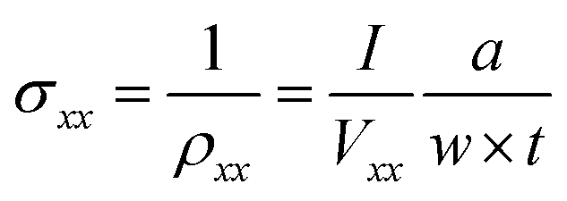 ) where w = 1 mm, a = 4 mm, and t = 100 nm are the channel width, distance between contacts, and film thickness, respectively. The leakage current was less than 2 nA, which is much less than the 1 μA that was applied during the measurements. The fluctuation of the temperature was less than 10 mK.
First principle calculations
For the first-principles calculations, the projector augmented wave (PAW) method26 of the Vienna ab initio simulation package (VASP)27 was used. The Perdew–Burke–Ernzerhof exchange–correlation functional (PBE)28 approach utilizing the generalized gradient approximation (GGA) scheme was employed, and the local spin density approximation (LSDA)+U method was used to compensate for the Coulomb interaction in the localized semi-core Zn-3d and Co-3d orbitals.29 We used U = 5 eV.Results and discussion
In our previous studies,20,25 we found that ferromagnetism in ZnCoO:H is proportional to the amount of hydrogen and cobalt. Since a very small amount of hydrogen was injected into the sample in this study, the sample was expected to show either a very weak ferromagnetic signal or not to exhibit ferromagnetism. This was confirmed from M–H curves with no hysteresis loop at 5 K and from Hall voltage measurements showing no traces of the anomalous Hall effect (see ESI Fig. S1†).In magnetotransport measurements, resistance values are obtained as a function of a changing magnetic field. In this study, resistance was measured as the gate voltage was varied from −20 V to 20 V for fixed magnetic fields ranging from 0 T to 3 T. Because the resistance for the negative magnetic field was nearly identical to that for the positive magnetic field with the same magnitude (see ESI Fig. S2†), we show only the results for the positive magnetic field. The resistivity ρxx was derived from  .
.
Fig. 1(a) shows the resistivity ρxx as a function of the gate voltage, VG, for various magnetic fields (0–3 T). When the magnetic field was 0 T, the resistivity increased initially with gate voltage, reached a maximum, and then decreased. As the magnetic field increased, the resistivity at the same gate voltage became larger, which indicates the positive magnetoresistance (MR). With increasing magnetic field up to 1.2 T, the dependency of the resistivity on the gate voltage showed tendencies similar to those at 0 T. Above 1.4 T, however, the behavior of the resistivity curve with respect to the gate voltage differed from that for lower magnetic fields. Near the maximum, a knee point was observed, in which the curvature of the resistivity changed and the interval between the maximum and knee point became larger.
 | ||
| Fig. 1 Resistivity results with the maximum and knee points. (a) Resistivity ρxx as a function of the gate voltage VG, as the magnetic field strength varied between 0 and 3 T. The resistivity increased initially, and then decreased as the gate voltage was changed from −20 V to 20 V. (b) Gate voltages with the maximum resistivity (black squares) and the knee point (red circles) as a function of the magnetic field. The knee point appears above 1.4 T. | ||
Fig. 1(b) shows the gate voltages for the maximum resistivity (black squares) and at the knee point (red circles) as a function of magnetic field. Upon increasing the magnetic field, the gate voltage at the maximum resistivity increased up to 1.4 T, and then decreased, thereby creating the knee point.
To study the magnetic field dependency of the resistivity in detail, the MR, defined as the normalized change in resistivity Δρ with respect to the resistivity at zero magnetic field, ρ0 i.e., the difference between the resistivities with and without the magnetic field, was evaluated.
Fig. 2(a) shows the MR as a function of gate voltage and magnetic field. Below 1.4 T, the MR increased initially as the gate voltage increased from −20 V, and then remained relatively constant as the gate voltage increased from ∼0 V to 20 V. Above 1.4 T, the MR showed a linear increase after a small anomaly, and maintained a constant value as the gate voltage continued to increase. Notably, the sudden jumps and drops of MR near VG = 11 V were caused by normalization with resistivity of the zero magnetic field, which has a sudden jump and drop near VG = 11 V, as indicated in the noise signals of Fig. 1(a); these abrupt changes have no physical meaning.
 | ||
| Fig. 2 Magnetoresistance (MR) as a function of gate voltage VG and magnetic field strength. (a) MR as a function of the voltage. (b) Comparison of MR and resistivity at 3 T. | ||
Fig. 2(b) shows the relationship between MR and resistivity at 3 T. As the gate voltage increased from VG = −20.0 V, the resistivity and MR increased up to VG = −15.0 V, in which a small anomaly in MR synchronized with the maximum in resistivity. Between −15.0 V and 0.0 V, the resistivity decreased linearly, while MR increased linearly. Above VG = 0.0 V, MR remained constant while the resistivity decreased.
To check the effects of gating on carrier density, the Hall coefficient and carrier density at each gate voltage were obtained from 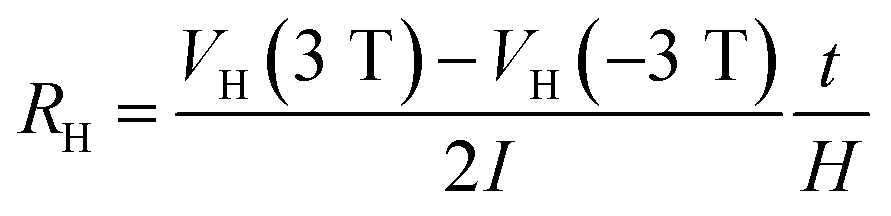 , with Hall voltages VH (3 T) and VH (−3 T) measured at 3 T and −3 T, respectively, as shown in Fig. 3. The Hall coefficient, RH, was positive for VG < −13.5 V, indicating that the carriers were holes, whereas it was negative for VG ≥ −13.5 V indicating that the carriers were electrons. The carrier density for VG = 0 V was −4.0 × 1017 cm−3; thus, the sample was not conductive. From the dependency of the resistivity on temperature, the insulating behavior was confirmed (not shown here).
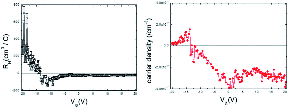 | ||
| Fig. 3 (a) Hall coefficient and (b) carrier density calculated from the Hall voltages at ±3 T. | ||
Fig. 3(b) shows that the carriers are holes for VG < −13.5 V, with a density less than 1.6 × 1017 cm−3. The type of carriers changed at VG = −13.5 V. This ambipolar behavior was also observed in hydrogen-incorporated ZnO nanowires.14 Under the assumption that the insulating layer Si3N4 has the ideal values of a dielectric constant of 7.5 and a thickness of 100 nm, the possible carrier density modulated by a gate voltage of 15.0 V is 6.23 × 1017 cm−3. This value is comparable with the carrier density derived from Hall measurements on ZnCoO:H.
To better understand the resistivity and MR results and ambipolar behavior, as they relate to carrier density and gate voltage, we considered the schematic model in Fig. 4 of the DOS of ZnCoO:H, with and without a magnetic field. We assumed that the Fermi energy was located slightly above the conduction band minimum (CBM) at VG = 0 V, with an impurity band with majority spin (spin up, red) located below the CBM in the case of a zero magnetic field (Fig. 4(a)).
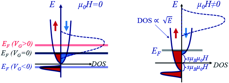 | ||
| Fig. 4 Schematic illustration of the density of states (DOS) of ZnCoO:H with a zero (a) and nonzero (b) magnetic field. When a magnetic field is applied, the energy bands of the spin-up (majority, red), and spin down (minority, blue), are split by Zeeman energy. The dashed curve represents an impurity band from a hybrid of Co-d and Zn-s electrons. | ||
Hybrids of Co-d and Zn-s electrons created an impurity band (dashed lines); however, because the carrier density of the sample is small, little amount of the carriers are attributed to this impurity band. Also, the magnetic field pushes this impurity band up, far above the Fermi energy, as shown in Fig. 4(b); thus, the contribution of this impurity band to the transport properties of the material is insignificant.
Using the assumed DOS shown (Fig. 4), the gate voltage dependency of the resistivity with zero field can be explained as follows. When a positive gate voltage is applied, the carrier density increases and the Fermi energy is raised into the conduction band, leading to a smaller resistivity. When a negative gate voltage is applied, resulting in a decrease of the carrier density, the Fermi energy is lowered into the impurity band through the CBM. When the Fermi energy is located at the CBM (in our case, VG = −14.2 V for zero magnetic field), the resistivity showed a maximum. The carriers are holes with low mobility when the Fermi energy is located in the impurity band below CBM.
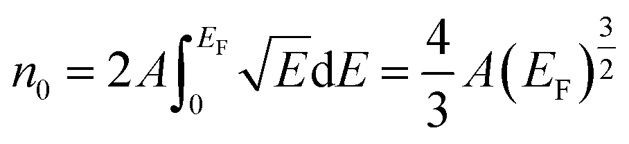
In Fig. 4(b), we consider a nonzero magnetic field. As shown in Fig. 1(a), for magnetic fields above 1.4 T, there was a knee point in which the slope of the resistivity changes with increasing gate voltage. This knee point of the resistivity can be explained by the Fermi energy being located at the CBM of the minority spin. When the Fermi energy is positioned above the CBM of the minority, electrons with both majority and minority spins participate in electrical transport. However, when the Fermi energy is located below the CBM of the minority, only electrons with the majority spin are involved in the electrical transport. Thus, the slope of the resistivity below the maximum is different from that of the resistivity between the maximum and knee point shown in Fig. 1(a). The fact that no knee points are observable for magnetic fields less than 1.4 T can be explained in terms of thermal energy. The thermal energy at 5 K was 0.43 meV, which is comparable to the magnetic field energy, 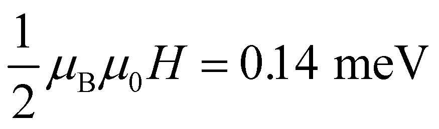 for μ0H = 1.4 T. Thus, for a small magnetic field whose magnetic field energy is smaller than the thermal energy, the splitting of the majority and minor spin energy bands is not clear, resulting in no knee points.
For simplicity, we assumed that the conduction band is an s-like band with a DOS proportional to the square root E and a spin of 1/2. So, the relation between the concentration of electrons and the Fermi energy at zero magnetic field is given by
 | (1) |
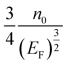 .
.
When a magnetic field is applied, the energy band is split according to the Zeeman energy, as shown in Fig. 4(b), and the concentrations of spin up (majority, red) and spin down (minority, blue) electrons depend on the Fermi energy, EF, and the magnetic field, H, as given below:
 | (2) |
 , and magnetic field energy,
  , where n0, EF0, s, μB, and μ0 represent the carrier density, the Fermi energy with the zero gate voltage, carrier spin, and the Bohr magneton and vacuum permeability, respectively.
Because the DOS of the impurity band is not simple, we considered carrier densities for which Fermi energy is located above the CBM of the majority spin.
The normalized total carrier density as a function of εF and εH is given as eqn (2) (and as shown in Fig. S3†):
 | (3) |
As discussed by Q. Xu,30 the positive MR of ZnCoO at low temperature is normally attributed to the spin-split conduction band. Spin spitting induces spin polarization. Thus MR and spin polarization are compared. The net spin polarization is given by
 | (4) |
Fig. 5(a) shows the net spin polarization Δn/n0 with respect to the normalized carrier density and magnetic field. The black squares and red circles mark the points with Δn = 0 and Δn = n, respectively. The dependency of the net spin polarization on the carrier density changes at the points (red circles) of Δn = n. Fig. 5(b) shows the experimental results of MR as a function of the gate voltage and magnetic field. The anomalies marked with black squares are the points where the curvature changes. The red circles correspond to the points where the slope of MR changes for μ0H ≥ 1.4 T. For a magnetic field, μ0H ≤ 1.2 T, MR increased monotonically and saturated without anomalous points as VG increased.
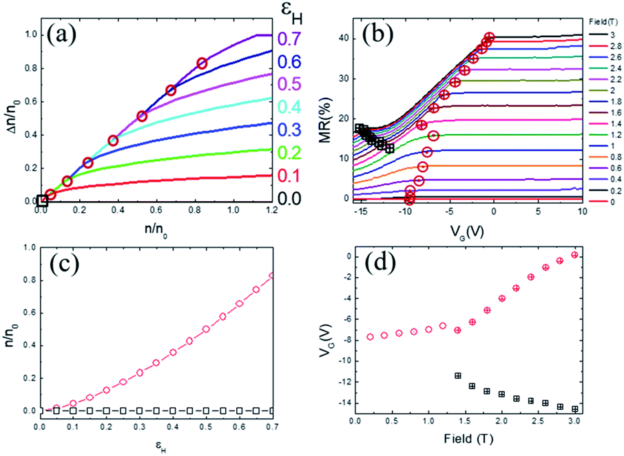 | ||
| Fig. 5 Comparison of the calculated spin polarization to experimental MR results. (a) Calculated net spin polarization Δn/n0 as a function of the normalized carrier density and (c) the points for Δn = 0 (black squares) and for Δn = n (red circles) where the dependency of Δn on n changes, respectively. (b) Experimental MR results as a function of the gate voltage and (d) the points of small anomalies and saturations. | ||
This absence of anomalous points may be explained by the thermal energy as before. For small magnetic fields with Zeeman energy comparable to the thermal energy, the Fermi energy is broadened in proportion to the thermal energy (wider than the Zeeman energy), which makes the anomalous points indistinct.
Fig. 5(c) and (d) show the points where the dependency of the net spin polarization and MR changes. The x-axes of the graphs in Fig. 5(c) and (d) are the normalized magnetic field energy and magnetic field; thus, the former corresponds to the latter. The y-axis of the graph in Fig. 5(c) represents the net spin polarization, which is also related to MR. The calculated results show the same tendency as the experimental MR results for μ0H ≥ 1.4 T, despite our simple assumption. The discrepancy of the curvatures, where Δn/n0 does not saturate at large n/n0 but MR saturates for a high VG, could be minimized by considering a more realistic DOS, as well as the thermal energy.
To determine the validity of the DOS assumed, we calculated the electronic structure of ZnO with Co–H–Co complexes and free Co ions using first-principles calculations; these calculations were performed using the projector augmented wave method of the Vienna ab initio simulation package;27 the detailed parameters for the calculation have been published elsewhere.25 The results are shown in Fig. 6.
 | ||
| Fig. 6 Calculated DOS for ZnO with two Co ions and H and the partial-DOS (p-DOS) from H and Co-3d orbitals. The positive (negative) values describe the majority (minority) spin state. | ||
One difference from the previous calculation25 is that a Co atom and a Co–H–Co molecule are located together in the supercell including 64 atoms, since two kinds of Co-driven structures are expected to be mixed in the real sample. From this calculation, we can discriminate the effects of a molecule of Co–H–Co and a single Co atom on the electronic structure. The present study focuses on the conduction band edge. It is remarkable that a spin-polarized peak from Co–H–Co is present just below the conduction band edge, and is nearly resonant to the CBM, consistent with Fig. 4. The isolated Co atom without the H coupling contributes little to spin-polarization near the CBM, since the s-d interaction is weak. The Co–H–Co state of the majority spin is empty normally, but can be occupied by electrons provided by the O-vacancy or by control of the gate voltage of the present TFT device. The calculated spin-polarized DOS around the CBM from the Co–H–Co is in good agreement with that obtained from the gate voltage dependence of the observed resistivity and MR. Thus, the present experimental data provide strong evidence for formation of the Co–H–Co molecule in ZnCoO:H.
In this letter, we did not show the Hall voltage data that exhibits fluctuations depending on the temperature and magnetic field. We expect that these fluctuations can be explained with the DOS proposed here and, as such, they will be addressed in the next paper.
Conclusions
The resistivity of hydrogenated ZnCoO was examined with respect to the gate voltage and magnetic field strength. From the dependency of the resistivity and MR on the gate voltage, a DOS for ZnCoO:H was proposed. For magnetic field strengths above 1.4 T, there was a knee point in which the slope of the resistivity changed with increasing gate voltage. This knee point of the resistivity can be explained by the Fermi energy being located at the CBM of the minority spin. When the Fermi energy is positioned above the CBM of the minority, both electrons with majority and minority spin participate in electrical transport; however, when the Fermi energy is located below the CBM of the minority, only electrons with majority spin are involved. Thus, the slope of the resistivity below the maximum is different from that of the resistivity between the maximum and knee point. The fact that no knee point was observable for magnetic fields less than 1.4 T can be explained in terms of thermal energy. The thermal energy at 5 K was 0.43 meV, which is comparable to the magnetic field energy, μBμ0H = 0.14 meV for μ0H = 1.4 T. Thus, for a small magnetic field whose magnetic field energy is smaller than the thermal energy, the splitting of the majority and minor spin energy bands is not clear, resulting in no knee points. The calculated net spin well reproduced the experimental MR results and the proposed DOS was consistent with the DOS obtained using first-principles calculations. These results provide clues regarding the possibility of gate voltage control of magnetic ordering using fine addition of H to ZnCoO.These results provide evidence for the presence of Co–H–Co in ZnCoO:H and show the possibility of investigating the electronic structure of the diluted magnetic semiconductors around the conduction band edge through the control of the gate voltage of TFT device.
Conflicts of interest
There are no conflicts to declare.Acknowledgements
This research was supported by Basic Science Research Program through the National Research Foundation of Korea (NRF) funded by the Ministry of Science, ICT & Future Planning (No. NRF-2017R1A2B3011822) and by the “2017 Post-Doc. Development Program” of Pusan National University. C. H. Park acknowledges the support of the National Research Foundation of Korea (NRF) grant funded by the Korean Government (2015M3D1A1070609).Notes and references
- M. A. Green, J. Appl. Phys., 1990, 67, 2944 CrossRef CAS.
- A. P. Alivisatos, Science, 1996, 271, 933–937 CAS.
- H. Shimotani, H. Asanuma, A. Tsukazaki, A. Ohtomo, M. Kawasaki and Y. Iwasa, Appl. Phys. Lett., 2007, 91, 082106 CrossRef.
- A. K. Geim and K. S. Novoselov, Nat. Mater., 2007, 6, 183–191 CrossRef CAS PubMed.
- K. S. Novoselov, A. K. Geim, S. V. Morozov, D. Jiang, Y. Zhang, S. V. Dubonos, I. V. Grigorieva and A. A. Firsov, Science, 2004, 306, 666–669 CrossRef CAS PubMed.
- Y. Zhang, T.-T. Tang, C. Girit, Z. Hao, M. C. Martin, A. Zettl, M. F. Crommie, Y. R. Shen and F. Wang, Nature, 2009, 459, 820–823 CrossRef CAS PubMed.
- V. L. Nguyen, D. J. Perello, S. Lee, C. T. Nai, B. G. Shin, J.-G. Kim, H. Y. Park, H. Y. Jeong, J. Zhao, Q. A. Vu, S. H. Lee, K. P. Loh, S.-Y. Jeong and Y. H. Lee, Adv. Mater., 2016, 28, 8177–8183 CrossRef CAS PubMed.
- S. Z. Bisri, C. Piliego, J. Gao and M. A. Loi, Adv. Mater., 2014, 26, 1176–1199 CrossRef CAS PubMed.
- J. Gao, F. J. Uribe-Romo, J. D. Saathoff, H. Arslan, C. R. Crick, S. J. Hein, B. Itin, P. Clancy, W. R. Dichtel and Y.-L. Loo, ACS Nano, 2016, 10, 4847–4856 CrossRef CAS PubMed.
- R. Martel, V. Derycke, C. Lavoie, J. Appenzeller, K. K. Chan, J. Tersoff and P. Avouris, Phys. Rev. Lett., 2001, 87, 256805 CrossRef CAS PubMed.
- J. Schornbaum, Y. Zakharko, M. Held, S. Thiemann, F. Gannott and J. Zaumseil, Nano Lett., 2015, 15, 1822–1828 CrossRef CAS PubMed.
- B. Kang, Y. Kim, J. H. Cho and C. Lee, 2D Materials, 2017, 4, 025014 CrossRef.
- B. N. Pal, P. Trottman, J. Sun and H. E. Katz, Adv. Funct. Mater., 2008, 18, 1832–1839 CrossRef CAS.
- A. Prasad, A. Pandey, V. K. Kunapuli, P. L. Bergstrom and Y. K. Yap, J. Phys. Chem. C, 2012, 116, 8210–8215 CAS.
- T. Dietl, H. Ohno, F. Matsukura, J. Cibert and D. Ferrand, Science, 2000, 287, 1019–1022 CrossRef CAS PubMed.
- H.-J. Lee, S.-Y. Jeong, C. R. Cho and C. H. Park, Appl. Phys. Lett., 2002, 81, 4020–4022 CrossRef CAS.
- K. Sato and H. Katayama-Yoshida, Jpn. J. Appl. Phys., 2000, 39, L555 CrossRef CAS.
- H.-J. Lee, C. H. Park, S.-Y. Jeong, K.-J. Yee, C. R. Cho, M.-H. Jung and D. J. Chadi, Appl. Phys. Lett., 2006, 88, 062504 CrossRef.
- R. K. Singhal, A. Samariya, S. Kumar, Y. T. Xing, U. P. Deshpande, T. Shripathi and E. S. Saitovitch, J. Magn. Magn. Mater., 2010, 322, 2187–2190 CrossRef CAS.
- C. H. Park and D. J. Chadi, Phys. Rev. Lett., 2005, 94, 127204 CrossRef CAS PubMed.
- M. H. N. Assadi, Y. B. Zhang and S. Li, J. Phys.: Condens. Matter, 2010, 22, 486003 CrossRef CAS PubMed.
- M. Khalid, M. Ziese, A. Setzer, P. Esquinazi, M. Lorenz, H. Hochmuth, M. Grundmann, D. Spemann, T. Butz, G. Brauer, W. Anwand, G. Fischer, W. A. Adeagbo, W. Hergert and A. Ernst, Phys. Rev. B: Condens. Matter Mater. Phys., 2009, 80, 035331 CrossRef.
- M. Cheon, Y. C. Cho, C.-R. Cho, C. H. Park and S.-Y. Jeong, RSC Adv., 2016, 6, 97555–97559 RSC.
- S. Lee, W.-K. Kim, Y. C. Cho, B.-S. Kim, Ji H. Park, C.-W. Lee, Y. P. Lee, S. B. Lee, S. Fackler, I. Takeuchi, C.R. Cho and S.-Y. Jeong, Appl. Phys. Lett., 2014, 104, 052405 CrossRef.
- Y. C. Cho, S. Lee, J. H. Park, W. K. Kim, H.-H. Nahm, C. H. Park and S.-Y. Jeong, New J. Phys., 2014, 16, 073030 CrossRef.
- P. E. Blöchl, Phys. Rev. B: Condens. Matter Mater. Phys., 1994, 50, 17953 CrossRef.
- G. Kresse and J. Furthműller, Phys. Rev. B: Condens. Matter Mater. Phys., 1996, 54, 11169–11186 CrossRef CAS.
- J. P. Perdew, K. Burke and M. Ernzerhof, Phys. Rev. Lett., 1996, 77, 3865 CrossRef CAS PubMed.
- V. I. Anisimov, J. Zaanen and O. K. Andersen, Phys. Rev. B: Condens. Matter Mater. Phys., 1991, 44, 943 CrossRef CAS.
- Q. Xu, L. Hartmann, H. Schmidt, H. Hochmuth, M. Lorenz, R. Schmidt-Grund, C. Sturm, D. Spemann and M. Grundmann, Phys. Rev. B: Condens. Matter Mater. Phys., 2006, 73, 205342 CrossRef.
Footnote |
| † Electronic supplementary information (ESI) available. See DOI: 10.1039/c7ra12866e |
| This journal is © The Royal Society of Chemistry 2018 |