
 Open Access Article
 This Open Access Article is licensed under a Creative Commons Attribution-Non Commercial 3.0 Unported Licence
Comparing the role of annealing on the transport properties of polymorphous AgBiSe2 and monophase AgSbSe2†
Minmin Zou *a,
Qing Liuab,
Chao-Feng Wuc,
Tian-Ran Weic,
Qing Tand,
Jing-Feng Lic and
Fei Chena
*a,
Qing Liuab,
Chao-Feng Wuc,
Tian-Ran Weic,
Qing Tand,
Jing-Feng Lic and
Fei Chena
aSchool of Materials Science and Engineering, Beijing Institute of Petrochemical Technology, Beijing, 102617, China. E-mail: zouminmin@bipt.edu.cn
bCollege of Materials Science and Engineering, Beijing University of Chemical Technology, Beijing 100029, China
cState Key Laboratory of New Ceramics and Fine Processing, School of Materials Science and Engineering, Tsinghua University, Beijing, 100084, China
dState Key Laboratory for Advanced Metals and Materials, University of Science and Technology Beijing, Beijing 100083, China
First published on 13th February 2018
Abstract
AgBiSe2 and AgSbSe2, two typical examples of Te-free I–V–VI2 chalcogenides, are drawing much attention due to their promising thermoelectric performance. Both compounds were synthesized via melting and consolidated by spark plasma sintering. The role of annealing on the transport properties of polymorphous AgBiSe2 and monophase AgSbSe2 was studied. Annealing has a greater impact on AgBiSe2 than AgSbSe2, which is ascribed to the temperature dependent phase transition of AgBiSe2. Unannealed AgBiSe2 shows p–n switching, but annealed AgBiSe2 exhibits n-type semiconducting behavior over the whole measurement temperature range. By performing high-temperature Hall measurements, we attribute this intriguing variation to the change in the amount of Ag vacancies and mid-temperature rhombohedral phase after annealing. Both AgBiSe2 and AgSbSe2 exhibit low thermal conductivity values, which are ∼0.40–0.50 W m−1 K−1 for AgSbSe2 and ∼0.45–0.70 W m−1 K−1 for AgBiSe2, respectively. The maximum ZT value of AgBiSe2 is enhanced from 0.18 to 0.21 after annealing. Pristine AgSbSe2 presents a ZT value as high as 0.60 at 623 K, although slight deterioration emerges after annealing.
Introduction
Nowadays the demand for replaceable clean energy is becoming urgent due to the shortage of non-renewable fossil fuels and ever-increasing serious environmental pollution. Thermoelectric materials, capable of converting waste heat to electrical energy, have received extensive interest.1–6 The energy conversion efficiency of a thermoelectric device is dependent on the dimensionless figure of merit (ZT) of the component materials. ZT is generally defined as ZT = α2T/ρκ, where T is the absolute temperature, α is the Seebeck coefficient, ρ is the electrical resistivity, and κ is the thermal conductivity.There are two feasible strategies to attain high ZT values. One is improving power factor (α2/ρ) by carrier optimization and band engineering,7,8 the other is reducing thermal conductivity by all-scale hierarchy design.9–11 In recent years, complex nanostructures were designed; nanoscale precipitates, second phase particles as well as nano dots were introduced in bulk materials. However, it is challenging to controllably and reproducibly prepare such materials with reduced dimensions. Besides, nanostructures may grow or dissolve during prolonged high temperature operation. Therefore, thermoelectric materials with intrinsically low thermal conductivity are particularly appealing, among which I–V–VI2 compounds (where I = Cu, Ag or alkali metal; V = Sb, Bi; and VI = S, Se, Te) emerge as new candidates.12–21 The intrinsically low lattice thermal conductivity (κl) of I–V–VI2 compounds arises from the strong lattice anharmonicity that is believed to associate with the lone pair electrons (s electrons) on the group V atoms.22–24 Among numerous I–V–VI2 compounds, AgSbTe2 is widely studied due to the low thermal conductivity and high Seebeck coefficient. AgSbTe2 alloys with GeTe (TAGS)25–27 and PbTe (LAST-m),28 are well known for their remarkable ZT values. However, the thermodynamic instability and the rarity of Te element hindered the development of AgSbTe2-based thermoelectric materials.
AgBiSe2 and AgSbSe2, as homologues of AgSbTe2, in which relatively less expensive and earth-abundant element Se is used to replace Te, seem to be more attractive. AgBiSe2 exhibits an intriguing temperature dependent phase transition behavior,12,13,15,29,30 which crystallizes in a hexagonal phase (space group P![[3 with combining macron]](https://www.rsc.org/images/entities/char_0033_0304.gif) m1, α phase) at room temperature. As temperature increases, AgBiSe2 undergoes a phase transition to rhombohedral phase (space group Rm, β phase) at ∼470 K and then to face-centered cubic phase (space group Fmm, γ phase) with disordered Ag and Bi positions at ∼580 K. In contrast, AgSbSe2 crystallizes in a cubic phase in the whole temperature range. Colloidal method has been adopted to prepare I–V–VI2 compounds, and high ZT values over unity were achieved in both pristine AgBiSe2 (ref. 13) and AgBi0.5Sb0.5Se2-based solid-solutioned homojunction nanoplates.31 Meanwhile, remarkable enhancement of thermoelectric performance was observed in solid-state route synthesized I–V–VI2 compounds through element doping, such as Nb/In doping13,14 at Ag site and anion (Cl/Br/I) doping29 at Se site in AgBiSe2, Pb/Bi/Cd/Na/Mg/Ba doping14,32–34 at Sb site and Sn doping35 at Se site in AgSbSe2, etc. To our surprise, AgBiSe2 synthesized by solution method is a p-type semiconductor at ambient temperature, and reversible p–n–p conduction type switching is also observed in as-prepared AgBiSe2.13,31 However, the Seebeck coefficient values of AgBiSe2 prepared via solid-state route indicate that AgBiSe2 is n-type semiconductor.15–17,29 Thus, the intrinsic transport behavior of AgBiSe2 is still an open issue worth further exploration.
m1, α phase) at room temperature. As temperature increases, AgBiSe2 undergoes a phase transition to rhombohedral phase (space group Rm, β phase) at ∼470 K and then to face-centered cubic phase (space group Fmm, γ phase) with disordered Ag and Bi positions at ∼580 K. In contrast, AgSbSe2 crystallizes in a cubic phase in the whole temperature range. Colloidal method has been adopted to prepare I–V–VI2 compounds, and high ZT values over unity were achieved in both pristine AgBiSe2 (ref. 13) and AgBi0.5Sb0.5Se2-based solid-solutioned homojunction nanoplates.31 Meanwhile, remarkable enhancement of thermoelectric performance was observed in solid-state route synthesized I–V–VI2 compounds through element doping, such as Nb/In doping13,14 at Ag site and anion (Cl/Br/I) doping29 at Se site in AgBiSe2, Pb/Bi/Cd/Na/Mg/Ba doping14,32–34 at Sb site and Sn doping35 at Se site in AgSbSe2, etc. To our surprise, AgBiSe2 synthesized by solution method is a p-type semiconductor at ambient temperature, and reversible p–n–p conduction type switching is also observed in as-prepared AgBiSe2.13,31 However, the Seebeck coefficient values of AgBiSe2 prepared via solid-state route indicate that AgBiSe2 is n-type semiconductor.15–17,29 Thus, the intrinsic transport behavior of AgBiSe2 is still an open issue worth further exploration.
It is well known that annealing treatment is a common method used to eliminate defects and to improve the uniformity of microstructure and distribution of composition. The thermoelectric performance will be stable after annealing and transport properties of annealed samples should be close to the intrinsic value. Although long-term annealing has been applied to LAST compounds,36,37 to our knowledge, the effect of annealing on polymorphous AgBiSe2 and monophase AgSbSe2 has not been reported yet.
In this work, we report the synthesis and thermoelectric properties of undoped AgBiSe2 and AgSbSe2. To gain an insight into the intrinsic transport behavior, annealing treatment was applied to the SPS-ed bulk samples, and high-temperature Hall measurement was used to investigate the temperature dependent carrier concentration of AgBiSe2. It is found that annealing has greater impact on polymorphous AgBiSe2 than monophase AgSbSe2, which is ascribed to the temperature dependent phase transition of AgBiSe2. Unannealed AgBiSe2 shows a p–n switching, but annealed AgBiSe2 exhibits n-type semiconducting behavior in the whole temperature range. The ZT value of AgBiSe2 is improved after annealing due to significant reduction in electrical resistivity, with a peak value of 0.21 at 673 K. AgSbSe2 displays better thermoelectric performance, and a maximum ZT value of 0.60 is achieved at 623 K, which slightly declines after annealing.
Experimental
Ingots of AgBiSe2 and AgSbSe2 were prepared by mixing stoichiometric Ag (99.95%), Bi (99.999%), Sb (99.999%) and Se (99.99%) in quartz tubes. The tubes were flame sealed under a high vacuum (∼10−4 Torr) and slowly heated to 673 K by 12 h, and then heated up to 1123 K in 4 h, soaked for 10 h, and subsequently cooled to room temperature. The as-prepared ingots were hand milled into powders by agate mortar. The derived powders were sintered in vacuum using a spark plasma sintering (SPS) system (Sumitomo SPS1010) under an axial compressive stress of 50 MPa at 673 K for 5 min. In order to study the effect of annealing on the thermoelectric performance of AgBiSe2 and AgSbSe2, the as-sintered samples were annealed in vacuum tube furnace at 673 K for 12 h.Structural investigations were carried out by X-ray diffractometry (XRD, Bruker D8 Advance, Germany) using Cu Kα radiation. Rietveld refinements were carried out using the GSAS II software.38 The average crystal structure of the AgBiSe2 was refined using the Pm1 space group and a minority Rm phase of AgBiSe2. Fit indicators: Rwp, Rexp, and χ2 were used to assess the quality of the refined structural models. The microscopic morphology and chemical composition of all samples were studied by field emission scanning electron microscopy (FE-SEM, Carl Zeiss Merlin, Germany) with energy dispersive X-ray spectrometer (EDS). The compositions were also measured by inductive coupled plasma emission spectrometer (ICP, IRIS Intrepid II XSP). The Seebeck coefficient and electrical resistivity were measured simultaneously on a ZEM-2 instrument system (Ulvac-Riko, Japan). The thermal conductivity was determined via κ = D × Cp × d, where D is the thermal diffusivity, Cp is the heat capacity, and d is the density. The thermal diffusivity was derived from the laser flash method (TC-9000, Ulvac-Riko, Japan). The heat capacity was estimated using the Dulong–Petit law, and the obtained values (Cp = 0.210 J g−1 K−1 for AgBiSe2 and Cp = 0.257 J g−1 K−1 for AgSbSe2) were close to the measured results.14,29 The density was measured by the Archimedes method. The Hall coefficients, RH, of the samples were characterized using a Hall coefficient measurement system (Resi-DC8340, Toyo, Japan). The Hall carrier concentration (nH) was calculated by nH = 1/eRH, where e is the electronic charge.
Results and discussion
Fig. 1 shows the XRD patterns of bulk AgBiSe2 and AgSbSe2 samples at different stage of preparation. AgSbSe2 crystallized in a cubic phase (PDF#65-6604) after melting. No obvious variation in the diffraction patterns is observed in both the samples after SPS and after annealing, except for slight broadening of the peaks. AgBiSe2 ingot crystallizes in a hexagonal phase (PDF#74-0842) after melting. The XRD patterns of AgBiSe2 are broadened and the relative intensity of (110) and (108) peak changes both after SPS and after annealing, which may originate from poor crystallinity of the SPS-ed sample compared with the ingot, or from the residual stress after SPS, or from the mixed phase constituent after SPS. On the one hand, the cooling rate of SPS is so fast that the high temperature cubic phase has not changed to hexagonal phase completely, thus a significant portion of the sample is frozen in the mid-temperature rhombohedral phase at room temperature. On the other hand, the lattice parameters of hexagonal phase (Pm1, a = 4.194 Å, c = 19.65 Å) and rhombohedral phase (Rm, a = 4.184 Å, c = 19.87 Å) are extremely close to each other,15 so it is hard to identify one from the other.
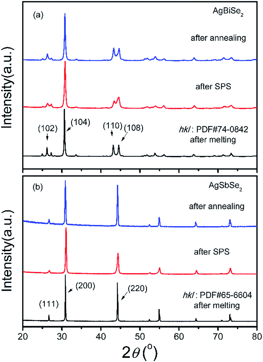 | ||
| Fig. 1 XRD patterns of bulk samples after melting, SPS and annealing, (a) AgBiSe2 and (b) AgSbSe2. | ||
Rietveld refinements were conducted to calculate the exact percentage of rhombohedral phase in all the AgBiSe2 samples. Fig. 2 shows the Rietveld refinement data of powder XRD patterns of AgBiSe2 obtained after melting, SPS and annealing. It should be noted that the XRD patterns of powder AgBiSe2 is slightly different from that of bulk AgBiSe2 samples, especially for the “after SPS” sample, which is mainly due to release of residual stress by grinding to powders. As shown in Fig. 2, the fractions of the rhombohedral phase are 10.6, 16.9 and 11%, respectively. The lattice parameters of AgBiSe2 are listed in Table S1.† Similar phenomenon was also observed by Böcher et al.17 It is reported that the fraction of the rhombohedral phase was ∼11–16% in all the Ag1−xBiSe2 samples revealed by the Rietveld refinement of synchrotron diffraction data. Above discussion leads us to a conclusion that a small quantity of mid-temperature rhombohedral phase exists in all the AgBiSe2 samples, and the proportion of rhombohedral phase decrease from 16.9% for unannealed AgBiSe2 to 11% for annealed AgBiSe2 due to the effect of annealing. Moreover, XRD patterns of bulk AgBiSe2 samples with different annealing process are shown in Fig. S1.† Except the sample cooling by water quenching, other samples show almost identical XRD patterns.
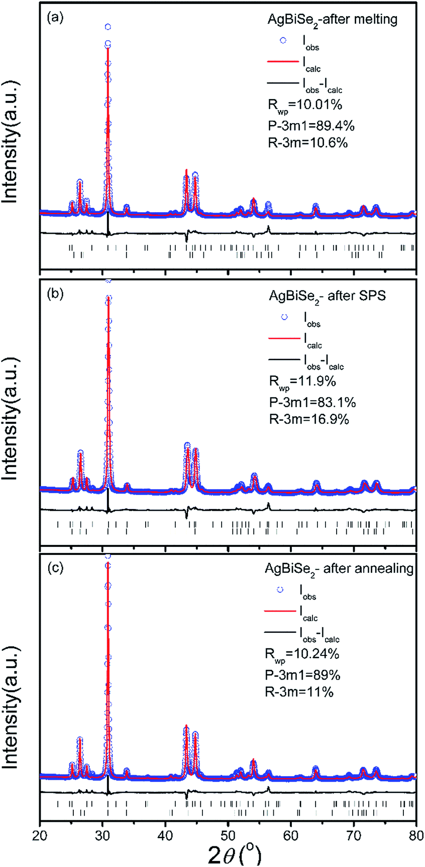 | ||
| Fig. 2 Rietveld refinement of powder XRD patterns of AgBiSe2 at different stage of preparation (a) after melting, (b) after SPS and (c) after annealing. | ||
The electrical resistivity of AgBiSe2 and AgSbSe2 prior to and after annealing is shown in Fig. 3(a). The resistivity of AgBiSe2 declines drastically after annealing, from 5.1 × 10⁴ μΩ m to 1.3 × 10³ μΩ m at 323 K, which can be ascribed to either the reduction of defects after annealing or the mild change in phase constituent as discussed above about the XRD results. In contrast, the electrical resistivity of AgSbSe2 increases after annealing, which may be attributed to the slight inevitable oxidation during the annealing process. The electrical resistivity of both annealed and unannealed AgBiSe2 initially decreases with increasing temperature below 480 K, then increases in the temperature range of 480–580 K, showing a metallic transport behavior, and finally decreases again above ∼580 K. Combining with the temperature dependent structural phase transition of AgBiSe2, it is easy to conclude that 480 K and 580 K correspond to the α–β and β–γ phase transition temperature, respectively. The reduction of electrical resistivity in AgBiSe2 above 580 K can be ascribed to the cubic phase crystallized at high temperature.
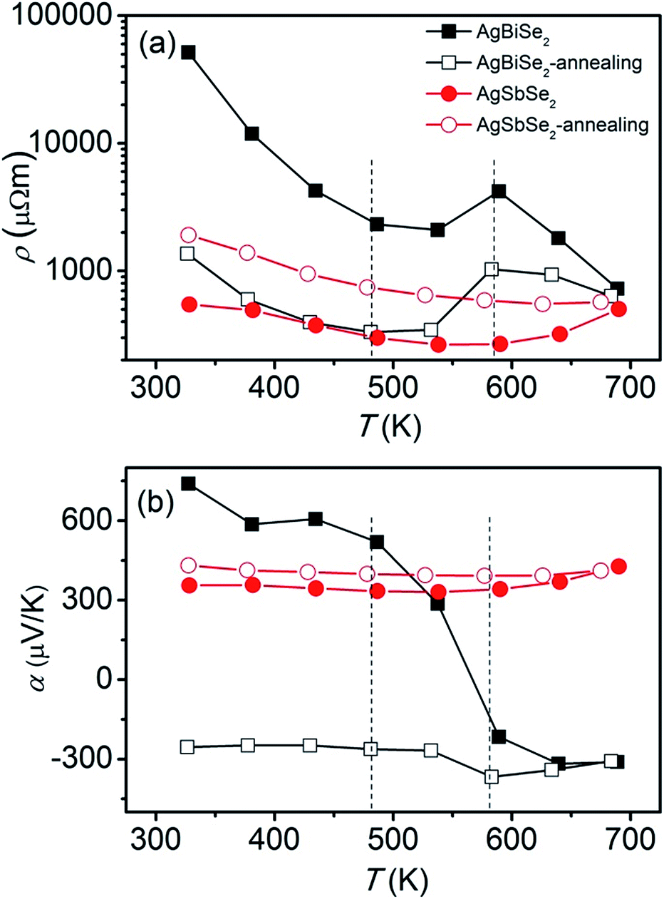 | ||
| Fig. 3 Temperature dependent (a) electrical resistivity and (b) Seebeck coefficient of AgBiSe2 and AgSbSe2 prior to and after annealing. The two vertical dotted lines are only guides for eyes. | ||
The Seebeck coefficient of AgBiSe2 and AgSbSe2 prior to and after annealing is shown in Fig. 3(b). The Seebeck coefficient of unannealed AgBiSe2 changes from positive to negative with increasing temperature, indicating that the majority carrier varies from hole to electron. Such p–n switching is also found in solution synthesized AgBiSe2,13 while the only difference is that we did not observe further n–p switching during the β–γ phase transition. The Seebeck coefficient of AgBiSe2 after annealing is negative in the entire temperature range, which suggests that electrons are the majority charge carrier in annealed AgBiSe2. |S| of AgBiSe2 after annealing remains flat blow 480 K, then increases markedly with increasing temperature, reaching the maximum value at 580 K, and then starts to decrease finally. The positive Seebeck coefficient of AgSbSe2 prior to and after annealing suggests that the carrier is dominated by hole in AgSbSe2, which are 355 μV K−1 and 431 μV K−1 at 323 K for AgSbSe2 before and after annealing, respectively. The relatively large Seebeck coefficient obtained in AgSbSe2 is related to the flat valence band maximum and multi-peak valence band structure.39
Considering that the variation of composition may lead to the change of transport behavior of AgBiSe2 after annealing, the microstructure and chemical composition of AgBiSe2 prior to and after annealing were investigated. Typical morphologies of fresh fracture surfaces for AgBiSe2 prior to and after annealing are exhibited in Fig. 4(a) and (b). It is interesting to find that the fracture model changes from predominantly transgranular fracture for unannealed AgBiSe2 to intergranular fracture for annealed AgBiSe2. The average grain size of annealed AgBiSe2 is ∼300–400 nm as displayed by the inset picture of Fig. 4(b). Elements of Ag, Bi and Se have a homogeneous distribution in annealed AgBiSe2 sample as shown in Fig. 4(c). The density and ICP composition of AgBiSe2 are listed in Table 1. Both samples have high density, which are 7.89 g cm−3 for unannealed AgBiSe2 and 7.88 g cm−3 for annealed AgBiSe2, corresponding to 98.6% and 98.5% of the theoretical density. Although the fracture surface of annealed AgBiSe2 seems more porous, the density is nearly unchanged. Because the “holes” are just left by pulling out other crystal grains, not real pores, as shown in the inset picture of Fig. 4(b). The ICP atomic ratios of Ag![[thin space (1/6-em)]](https://www.rsc.org/images/entities/char_2009.gif) :Bi:Se for unannealed AgBiSe2 and annealed AgBiSe2 are similar, and the ratio values are close to the nominal value. The slight deviation from stoichiometric ratio of Se in both samples may be attributed to the volatilization during fabrication process. Thus, it is supposed that the variation of composition is too small to influence the transport behavior of AgBiSe2.
:Bi:Se for unannealed AgBiSe2 and annealed AgBiSe2 are similar, and the ratio values are close to the nominal value. The slight deviation from stoichiometric ratio of Se in both samples may be attributed to the volatilization during fabrication process. Thus, it is supposed that the variation of composition is too small to influence the transport behavior of AgBiSe2.
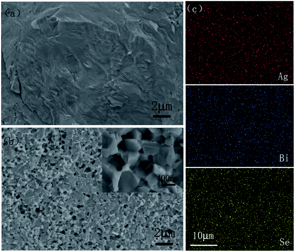 | ||
| Fig. 4 SEM images of fracture surface for (a) unannealed AgBiSe2 and (b) annealed AgBiSe2; (c) EDS mapping for the elements Ag, Bi and Se of annealed AgBiSe2. The inset picture in (b) is the high magnification image of annealed AgBiSe2. | ||
| Samples | Density (g cm−3) | ICP atomic ratio Ag:Bi:Se |
|---|---|---|
| AgBiSe2 | 7.89 | 25.08:25.28:49.64 |
| AgBiSe2-annealing | 7.88 | 24.84:25.66:49.50 |
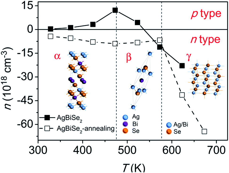
In order to clarify the extraordinary change in the Seebeck coefficient of AgBiSe2, high-temperature Hall coefficient measurement was conducted. The temperature dependent Hall carrier concentration of AgBiSe2 prior to and after annealing is plotted in Fig. 5. It should be noted that the sign of the carrier concentration is just used to represent the type of the majority carrier (negative for electron, positive for hole). What should also be declared is that the measurement uncertainty is about 5% for most temperature points, while the uncertainty could be 15–20% at 573 K, which might be ascribed to the undergoing β–γ phase transition at that temperature. Thus, the Hall carrier concentration at 573 K might be not so precise. Nevertheless, the trend of carrier concentration is still persuasive. Obviously, hole is the majority carrier below ∼523 K in unannealed AgBiSe2, but electron is predominant above ∼523 K, which offers solid evidence for the p–n switching behavior. The majority carrier of AgBiSe2 changes from hole to electron after annealing, which is consistent with the tendency of Seebeck coefficient. Typically, the Hall carrier concentration changes from 1.34 × 1017 cm−3 (hole) for unannealed AgBiSe2 to 3.74 × 1018 cm−3 (electron) for annealed AgBiSe2 at 323 K. Similar electron concentration of 5.85 × 1018 cm−3 was obtained by Guin et al. in pristine AgBiSe2.29 Pan et al. also reported a high electron concentration of 1.5 × 1019 cm−3 in n-type AgBiSe2.15 Regardless of carrier type, the Hall carrier concentration of both samples increases with increasing temperature below ∼480 K, then decreases in the rhombohedral phase temperature range, and finally increases above 580 K, displaying close connection with the temperature dependent phase transition of AgBiSe2. Mid-temperature rhombohedral phase AgBiSe2 is a semiconductor, whereas the high-temperature cubic phase with disordered arrangements of Ag and Bi atoms is found to be metallic.30 Thereby, the electrical transport behavior exhibits a semiconducting to metallic transition when going from rhombohedral to cubic phase, leading to the remarkable enhancement of carrier concentration above 580 K. Based on the variation of carrier concentration, the trends of electrical resistivity and Seebeck coefficient of AgBiSe2 can be well understood. Combining the results of electrical resistivity and Seebeck coefficient with carrier concentration, the possible reason for the distinct change of electrical transport behavior after annealing can be explained as following: (1) amount of defects exist in the SPS-ed AgBiSe2 sample, such as Ag vacancies, which act as hole dopants in AgBiSe2, leading to p-type transport behavior;13 (2) the existence of mid-temperature rhombohedral phase may contributes to the high electrical resistivity of unannealed AgBiSe2, for the rhombohedral phase has a higher electrical resistivity than the hexagonal phase;16 (3) it is well known that annealing plays an important role in eliminating defects and reducing unstable phase, thus the intrinsic n-type behavior and reduced electrical resistivity possibly turns out after annealing. Therefore, we reckon that the electrical properties of unannealed AgBiSe2 may not adequately reflect the original transport behavior, while the electrical properties of annealed AgBiSe2 should be close to the intrinsic properties.
 | ||
| Fig. 5 Temperature dependent Hall carrier concentration of AgBiSe2 prior to and after annealing. The two vertical dotted lines are only guides for eyes. | ||
To calculate the effective mass m* of annealed AgBiSe2, the carrier concentration (n) should be figured out first, because what we've got by Hall measurement system is the Hall carrier concentration (nH). The Hall carrier concentration nH is related to the carrier concentration n via nH = n/rH, where the Hall factor rH for acoustic phonon scattering is expressed by:
 | (1) |
 | (2) |
 | (3) |
 | (4) |
The power factor of AgBiSe2 and AgSbSe2 is plotted in Fig. 6. Unannealed AgSbSe2 exhibits the largest power factor, with a peak value of 437 μW m−1 K−2 at 590 K. However, the power factor of AgSbSe2 decreases after annealing due to the enhancement of electrical resistivity. Unannealed AgBiSe2 and annealed AgBiSe2 have the same variation trend of power factor: it increases with increasing temperature below 480 K, then decreases in the γ phase temperature range, and finally increases again above 580 K. Although the power factor of AgBiSe2 increases after annealing in the entire temperature range, the maximum value 207 μW m−1 K−2 at 480 K is still relatively low.
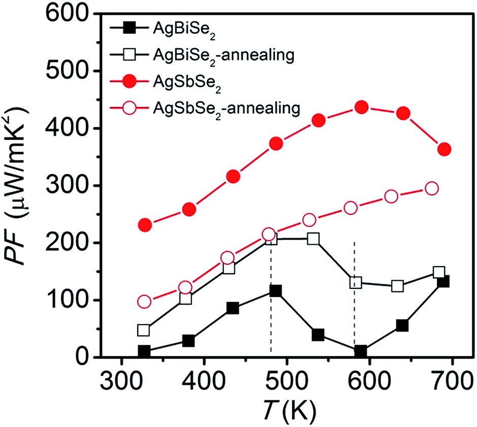 | ||
| Fig. 6 Temperature dependent power factor of AgBiSe2 and AgSbSe2 prior to and after annealing. The two vertical dotted lines are only guides for eyes. | ||
Fig. 7 shows the thermal conductivity prior to and after annealing for AgBiSe2 and AgSbSe2. All samples exhibit low thermal conductivity, less than 0.7 W m−1 K−1. Typically, the room temperature thermal conductivity values of annealed AgBiSe2 and annealed AgSbSe2 are 0.62 and 0.48 W m−1 K−1, respectively. Such low thermal conductivity in I–V–VI2 semiconductors is due to the large lattice anharmonicity arising from the lone pair electrons of Bi or Sb.22 The thermal conductivity of AgSbSe2 is even lower compared with AgBiSe2, in the range of 0.44–0.48 W m−1 K−1. The effect of annealing on the thermal conductivity of AgBiSe2 and AgSbSe2 is not as prominent as that on the electrical properties. The thermal conductivity of AgBiSe2 is slightly reduced after annealing, and that of AgSbSe2 remains substantially unchanged. Moreover, similar temperature dependence is observed in the thermal conductivity of AgBiSe2, as what we have found in electrical properties previously.
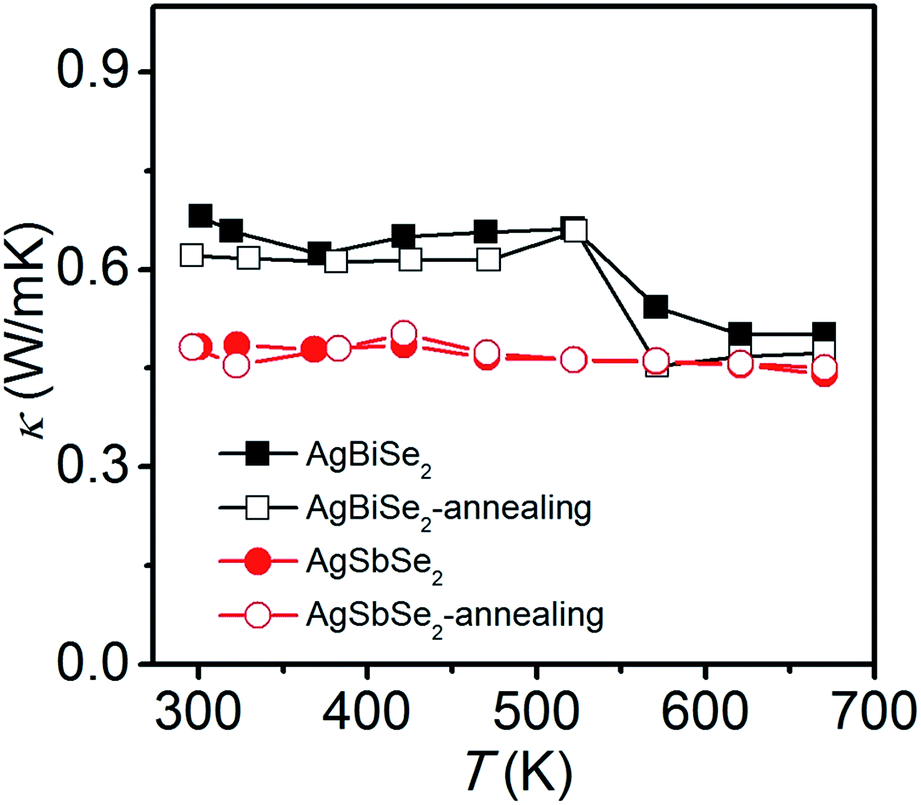 | ||
| Fig. 7 Temperature dependent thermal conductivity of AgBiSe2 and AgSbSe2 prior to and after annealing. | ||
The temperature dependent ZT values derived from the combination of the electrical and thermal transport properties are plotted in Fig. 8. AgSbSe2 samples have larger ZT values than AgBiSe2 over the entire investigated temperature range. A maximum ZT value of 0.60 is obtained in unannealed AgSbSe2 at 640 K. However, the peak ZT value of annealed AgSbSe2 is reduced to 0.44 at 675 K, which is mainly due to the enhancement of electrical resistivity. ZT value of AgBiSe2 increases after annealing, especially in the temperature range of 480–640 K. Typically, the peak ZT value of AgBiSe2 is improved from 0.18 to 0.21 after annealing.
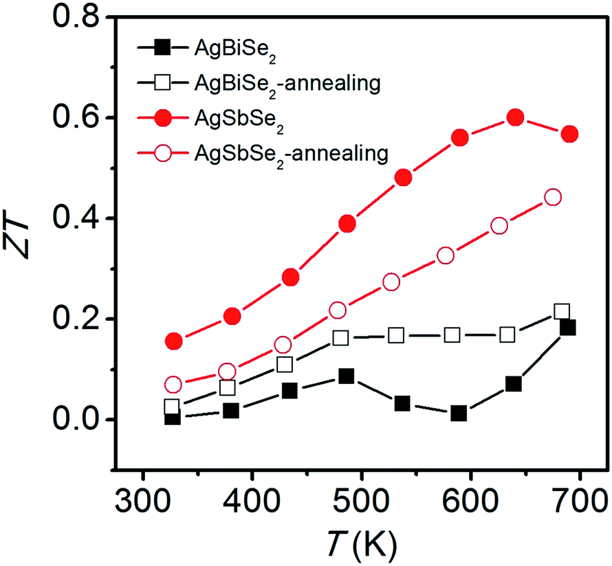 | ||
| Fig. 8 Temperature dependent ZT of AgBiSe2 and AgSbSe2 prior to and after annealing. | ||
Conclusions
In summary, AgBiSe2 and AgSbSe2 were synthesized by melting the mixture of elemental powders, annealing treatment was applied on the bulk samples after SPS. Annealing treatment has a great impact on thermoelectric properties of AgBiSe2 due to the intriguing temperature dependent phase transition. A p–n conduction type switching is observed in unannealed AgBiSe2, but electrons become the majority carrier after annealing. We reckon that the intrinsic transport behavior of AgBiSe2 should be n-type, and the p-type behavior and high electrical resistivity of unannealed AgBiSe2 might be caused by amount of Ag vacancies introduced via fabrication and the existence of mid-temperature rhombohedral phase after SPS. The peak ZT values are 0.18 and 0.21 for unannealed and annealed AgBiSe2, respectively. AgSbSe2 shows better thermoelectric performance than AgBiSe2 over the entire investigated temperature range. A relatively high ZT value of 0.60 is achieved for unannealed AgSbSe2, despite mild deterioration is observed after annealing. These findings in this work will provide an alternative way to understand the transport properties of AgBiSe2 and other I–V–VI2 compounds with phase transition. The thermoelectric performance of AgBiSe2 and AgSbSe2 are expected to be further enhanced by doping and/or nanostructuring.Conflicts of interest
There are no conflicts of interest to declare.Acknowledgements
This work was supported by the National Natural Science Foundation of China (Grant No. 51401025) and Training Program Foundation for the Beijing Municipal Excellent Talents (No. 2013D005005000004).References
- C. Wood, Rep. Prog. Phys., 1988, 51, 459–539 CrossRef CAS.
- G. J. Snyder and E. S. Toberer, Nat. Mater., 2008, 7, 105–114 CrossRef CAS PubMed.
- J. F. Li, W. S. Liu, L. D. Zhao and M. Zhou, NPG Asia Mater., 2010, 2, 152–158 CrossRef.
- L.-D. Zhao, V. P. Dravid and M. G. Kanatzidis, Energy Environ. Sci., 2014, 7, 251–268 CAS.
- T. Zhu, Y. Liu, C. Fu, J. P. Heremans, J. G. Snyder and X. Zhao, Adv. Mater., 2017, 29, 1605884 CrossRef PubMed.
- J.-f. Li, Y. Pan, C. F. Wu, F. H. Sun and T. R. Wei, Sci. China: Technol. Sci., 2017, 60, 1347–1364 CrossRef.
- J. P. Heremans, B. Wiendlocha and A. M. Chamoire, Energy Environ. Sci., 2012, 5, 5510–5530 CAS.
- Y. Pei, H. Wang and G. J. Snyder, Adv. Mater., 2012, 24, 6125–6135 CrossRef CAS PubMed.
- J. R. Sootsman, D. Y. Chung and M. G. Kanatzidis, Angew. Chem., Int. Ed., 2009, 48, 8616–8639 CrossRef CAS PubMed.
- M. G. Kanatzidis, Chem. Mater., 2010, 22, 648–659 CrossRef CAS.
- Y. C. Lan, A. J. Minnich, G. Chen and Z. F. Ren, Adv. Funct. Mater., 2010, 20, 357–376 CrossRef CAS.
- C. Manolikas and J. Spyridelis, Mater. Res. Bull., 1977, 907–913 CrossRef CAS.
- C. Xiao, X. M. Qin, J. Zhang, R. An, J. Xu, K. Li, B. X. Cao, J. L. Yang, B. J. Ye and Y. Xie, J. Am. Chem. Soc., 2012, 134, 18460–18466 CrossRef CAS PubMed.
- S. N. Guin, A. Chatterjee, D. S. Negi, R. Datta and K. Biswas, Energy Environ. Sci., 2013, 6, 2603–2608 CAS.
- L. Pan, D. Berardan and N. Dragoe, J. Am. Chem. Soc., 2013, 135, 4914–4917 CrossRef CAS PubMed.
- X. Liu, D. Jin and X. Liang, Appl. Phys. Lett., 2016, 109, 133901 CrossRef.
- F. Böcher, S. P. Culver, J. Peilstöcker, K. S. Weldert and W. G. Zeier, Dalton Trans., 2017, 46, 3906–3914 RSC.
- H. Wang, J. F. Li, M. M. Zou and T. Sui, Appl. Phys. Lett., 2008, 93, 202106 CrossRef.
- J. He, J. Xu, X. Tan, G.-Q. Liu, H. Shao, Z. Liu, H. Jiang and J. Jiang, Journal of Materiomics, 2016, 2, 165–171 CrossRef.
- S. Guin, S. Banerjee, D. Sanyal, S. Pati and K. Biswas, Chem. Mater., 2017, 29, 3769–3777 CrossRef CAS.
- S. Guin and K. Biswas, Chem. Mater., 2013, 25, 3225–3231 CrossRef CAS.
- D. T. Morelli, V. Jovovic and J. P. Heremans, Phys. Rev. Lett., 2008, 101, 035901 CrossRef CAS PubMed.
- M. D. Nielsen, V. Ozolins and J. P. Heremans, Energy Environ. Sci., 2013, 6, 570–578 CAS.
- S. N. Guin, D. S. Negi, R. Datta and K. Biswas, J. Mater. Chem. A, 2014, 2, 4324–4331 CAS.
- B. A. Cook, M. J. Kramer, X. Wei, J. L. Harringa and E. M. Levin, J. Appl. Phys., 2007, 101, 053715 CrossRef.
- S. H. Yang, T. J. Zhu, T. Sun, S. N. Zhang, X. B. Zhao and J. He, Nanotechnology, 2008, 19, 245707 CrossRef CAS PubMed.
- J. R. Salvador, J. Yang, X. Shi, H. Wang and A. A. Wereszczak, J. Solid State Chem., 2009, 182, 2088–2095 CrossRef CAS.
- K. F. Hsu, S. Loo, F. Guo, W. Chen, J. S. Dyck, C. Uher, T. Hogan, E. K. Polychroniadis and M. G. Kanatzidis, Science, 2004, 303, 818–821 CrossRef CAS PubMed.
- S. N. Guin, V. Srihari and K. Biswas, J. Mater. Chem. A, 2015, 3, 648–655 CAS.
- P. Larson and S. D. Mahanti, Annual March Meeting, American Physical Society, March 12–16, 2001 Search PubMed.
- C. Xiao, J. Xu, B. X. Cao, K. Li, M. G. Kong and Y. Xie, J. Am. Chem. Soc., 2012, 134, 7971–7977 CrossRef CAS PubMed.
- Z. Liu, J. Shuai, H. Geng, J. Mao, Y. Feng, X. Zhao, X. Meng, R. He, W. Cai and J. Sui, ACS Appl. Mater. Interfaces, 2015, 7, 23047–23055 CAS.
- S. N. Guin, A. Chatterjee and K. Biswas, RSC Adv., 2014, 4, 11811–11815 RSC.
- S. Cai, Z. Liu, J. Sun, R. Li, W. Fei and J. Sui, Dalton Trans., 2015, 44, 1046–1051 RSC.
- D. Li, X. Y. Qin, T. H. Zou, J. Zhang, B. J. Ren, C. J. Song, Y. F. Liu, L. Wang, H. X. Xin and J. C. Li, J. Alloys Compd., 2015, 635, 87–91 CrossRef CAS.
- M. Zhou, J. F. Li and T. Kita, J. Am. Chem. Soc., 2008, 130, 4527–4532 CrossRef CAS PubMed.
- J. Dadda, E. Müller, S. Perlt, T. Höche, P. Bauer Pereira and R. P. Hermann, J. Mater. Res., 2011, 26, 1800–1812 CrossRef CAS.
- B. H. Toby and R. B. Von Dreele, J. Appl. Crystallogr., 2013, 46, 544–549 CrossRef CAS.
- K. Hoang, S. D. Mahanti, J. R. Salvador and M. G. Kanatzidis, Phys. Rev. Lett., 2007, 99, 156403 CrossRef PubMed.
Footnote |
| † Electronic supplementary information (ESI) available. See DOI: 10.1039/c7ra12819c |
| This journal is © The Royal Society of Chemistry 2018 |