
 Open Access Article
 This Open Access Article is licensed under a Creative Commons Attribution-Non Commercial 3.0 Unported Licence
Change in crystalline structure of W18O49 nanowires induced by X-ray irradiation and its effects on field emission
Junqing Wu ab,
Bo Wangc,
Futing Yic,
Shaozhi Denga,
Ningsheng Xua and
Jun Chen*a
ab,
Bo Wangc,
Futing Yic,
Shaozhi Denga,
Ningsheng Xua and
Jun Chen*a
aState Key Lab of Optoelectronic Materials and Technologies, Guangdong Province Key Lab of Display Material and Technology, School of Electronics and Information Technology, Sun Yat-sen University, Guangzhou, 510275, People's Republic of China. E-mail: stscjun@mail.sysu.edu.cn
bJiangxi Province Key Lab of Microstructure Function Materials, Jiujiang Key Lab of Novel Function Nanomaterials, School of Science, Jiujiang University, Jiujiang, 332005, People's Republic of China
cInstitute of High Energy Physics, Chinese Academy of Sciences, Beijing, 100049, People's Republic of China
First published on 3rd January 2018
Abstract
W18O49 nanowires were synthesized by thermal evaporation, and the effects of X-ray irradiation on their crystalline structure, chemical composition, and field emission properties were systematically investigated. High-energy X-ray irradiation created nanoprotrusions on the surface of W18O49 nanowires and introduced crystalline slipping in the lattice. X-ray photoelectron spectroscopy results showed that the content of lattice oxygen increased and nitrogen was incorporated into the W18O49 nanowires after X-ray irradiation. Nevertheless, a stable and high current emission still could be obtained from the W18O49 nanowires after X-ray irradiation, with a slight increase in the threshold field from 6.4 to 7.9 MV m−1. The mechanism of the change in crystalline structure, chemical composition, and field emission performance of W18O49 nanowires induced by X-ray irradiation is discussed.
1. Introduction
Field emission cold cathodes have the advantages of spontaneous start-up, low-power consumption and long lifetime. They have wide application in field emission displays, microwave and radio-frequency tubes, scientific instruments and space electric propulsion, etc.1 Because their high aspect ratio is beneficial to field electron emission, carbon nanotubes have been widely studied for cold cathode application since their discovery. Excellent field emission properties have been reported and the field emission displays using carbon nanotubes have been demonstrated.2,3 At the same time, much attention has also been paid to other one-dimensional nanomaterials, such as ZnO nanowires, SnO2 nanowhiskers, CuO nanowires, GaN nanowires, W18O49 nanowires, etc.4–8Tungsten oxide is an n-type semiconductor material with promising physical and chemical properties and has been widely studied because of its potential application as gas sensors, photo-catalysts, information displays, photovoltaic conversion, and others.9–13 Tungsten oxide with nanoscale dimensions will display enhanced properties and can further widen its practical application range. Therefore, quasi-one-dimensional tungsten oxide nanomaterials have been prepared recently by various methods.14–18 Because of the high aspect ratio of its nanostructure and good electrical properties, the field emission properties of tungsten oxide nanomaterials have attracted much attention. Excellent field emission performance, including low turn-on field, high current density, good stability, and high uniformity, has been reported for various one-dimensional tungsten oxide nanomaterials.19–29 For example, in 2003, Li et al. reported that W18O49 nanotubes and nanowires can be prepared by heating tungsten foil under vacuum conditions and investigated their field emission properties; the turn-on field was only 2.6 MV m−1.19 Zhou et al. used two thermal evaporation processes to grow W18O49 nanotips; stable field emission with fluctuation of 2.0% at an emission current of 1200 μA over 13 hours and a low turn-on field of 2.0 MV m−1 were obtained.20,21 Single-crystalline WO3 nanowires on carbon paper substrates are excellent field emitters: an ultralow turn-on field of 1.8 MV m−1 and threshold field of 3.3 MV m−1 have been shown, and the field emission current density reached up to 40 mA cm−2.22 On the other hand, improvements in the field mission performance of tungsten oxide nanomaterials have also been studied, such as tuning the ratio of WO2 and WO2.9,24 electric treatment,25 and plasma treatment.26 The effect of environment temperature27,28 and atomic oxygen exposure29 on the field emission properties of tungsten oxide nanowires have also been reported in attempts to determine the emission mechanism of metal oxide field emitters.
These results show that tungsten oxide nanomaterial is a promising material for application as a field emitter. In some applications, field emitters can be exposed to harsh environments. For example, there is a possible high flux of high energy X-ray irradiation in space. Determining how the high-energy X-ray irradiation affects the crystalline structure and field electron emission properties of tungsten oxide nanomaterials is an important issue for practical application. However, there has been little research on this important issue,30–32 which still remains an open question. In this paper, W18O49 nanowires were prepared by thermal evaporation and then irradiated by high-energy X-rays. We focused on the effects of X-ray irradiation on the crystalline structure, chemical composition, and field emission properties of W18O49 nanowires to evaluate its radiation resistance as a field emitter. The corresponding mechanism is also discussed.
2. Experimental
Large-scale, high-density, and vertically aligned W18O49 nanowires were grown on n-type silicon substrates (electrical resistivity: 0.1 Ω cm) by thermal evaporation of tungsten powder (China Nonferrous Metal Co., purity: 99.5%).26 The X-ray irradiation was carried out using synchrotron radiation at the Beijing Synchrotron Radiation Facility (BSRF). The beam is composed of X-rays with energy in the range of 3–16 keV, and the flux is ∼1012 phs (cm2 s)−1. The three irradiation times used in this study were 5 min, 15 min, and 60 min, and the corresponding irradiation doses were 3 × 10¹⁴, 9 × 10¹⁴, and 3.6 × 10¹⁵ phs cm−2, respectively. During irradiation, the samples were positioned in a vacuum chamber with a pressure of 5 Pa.A scanning electron microscope (SEM, Zeiss Supra 55) was used to observe the morphology of W18O49 nanowires. A transmission electron microscope (TEM, JEM-2010HR) and X-ray diffraction (XRD, D-MAX 2200 VPC) were used to characterize the crystalline structure of W18O49 nanowires. The composition of W18O49 nanowires was analyzed by X-ray photoelectron spectroscopy (XPS, ESCALAB 250) and energy-dispersive X-ray spectroscopy (EDS). Field emission measurements were carried out in an ultra-high vacuum chamber with a base pressure of ∼1 × 10⁻⁶ Pa using an anode probe technique. The diameter of the probe was 5 mm. The distance between the anode and the cathode was 300 μm.
3. Results and discussion
A. Characterization of W18O49 nanowires before and after X-ray irradiation
Fig. 1(a–c) shows typical SEM images of W18O49 nanowires with top-view and cross-section views. The W18O49 nanomaterial was in the form of nanowires. High-density W18O49 nanowires were vertically aligned on n-type silicon substrates. The diameter and height of W18O49 nanowires were approximately 20–50 nm and 4–6 μm, respectively. Fig. 1(d) shows EDS spectrum of W18O49 nanowires. Four elements (O, W, C, and Si) were found in the as-prepared samples, and the atomic ratio is shown in the inset. The Si signal is from the silicon substrate, and the C signal is due to surface-adsorbed carbon. The EDS results showed that the composition of the nanowires was tungsten oxide. Fig. 1(e) shows the XRD pattern of the tungsten oxide nanowires. Two obvious peaks at 23.54° and 48.10° were observed, which can be indexed to lattice planes (010) and (020) of the monoclinic W18O49 phase (JCPDS card no. 36-101), respectively. Thus, it can be concluded that the prepared nanowires were made of pure W18O49 with a monoclinic structure and their alignment was very good, which is consistent with the SEM results.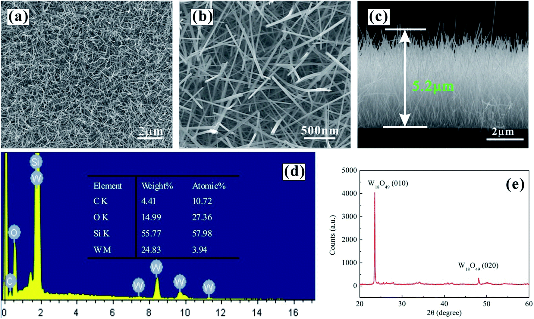 | ||
| Fig. 1 SEM images of as-grown W18O49 nanowires: (a) (b) top view, (c) cross-section view, (d) EDS spectrum, and (e) XRD pattern. | ||
Fig. 2 shows the XRD pattern of as-grown and irradiated W18O49 nanowires. The XRD pattern of irradiated W18O49 nanowires was almost the same as that of the as-grown W18O49 nanowires, which indicated that chemical structure of W18O49 nanowires remained unchanged after X-ray irradiation. The morphology of W18O49 nanowires before and after X-ray irradiation was also characterized, and the results are shown in the inset of Fig. 2. No change was found in the morphology of W18O49 nanowires after X-ray irradiation.
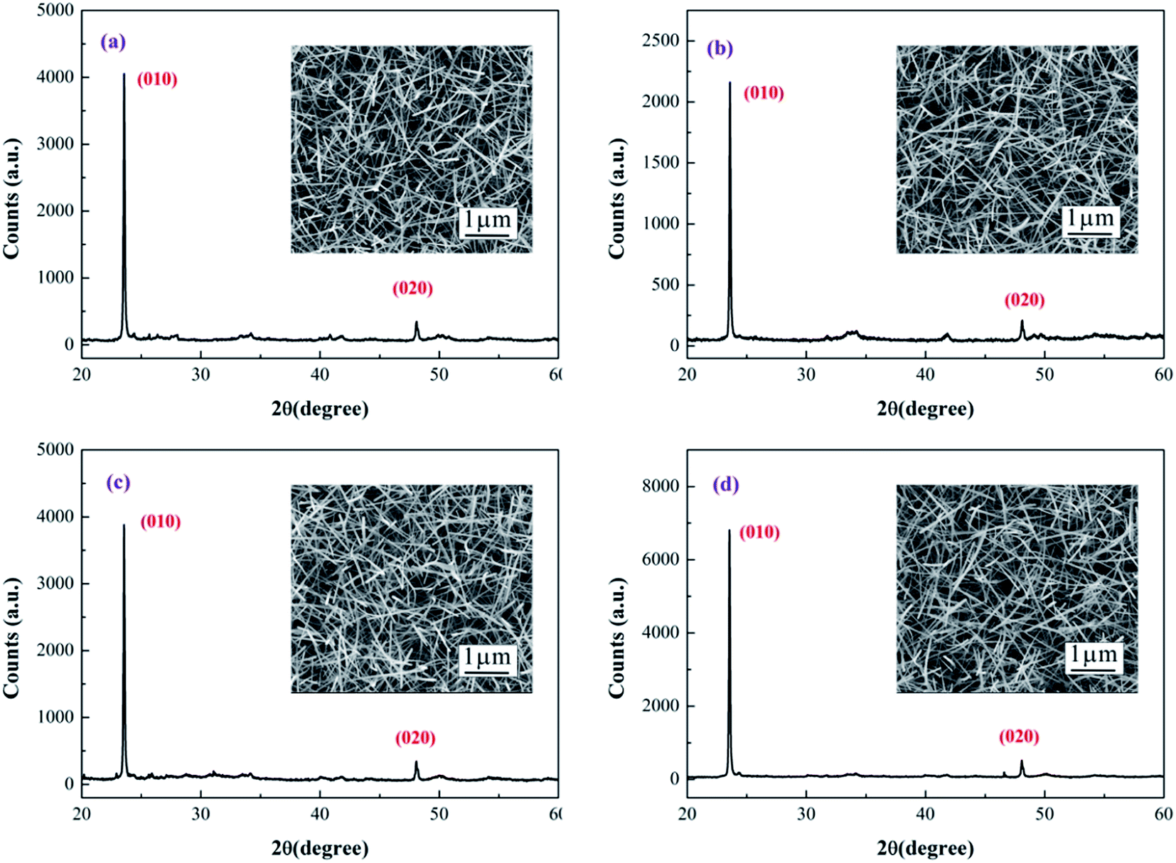 | ||
| Fig. 2 XRD patterns of as-grown and irradiated W18O49 nanowires. The inset shows corresponding SEM images. | ||
Fig. 3 shows typical TEM images of as-grown and irradiated W18O49 nanowires. Two obvious changes in crystalline structure were found after X-ray irradiation. First, the surface of the as-grown W18O49 nanowires was relatively smooth, and no obvious amorphous layer was found (Fig. 3(a)). For irradiated W18O49 nanowires, the surface of the nanowire was covered by an amorphous layer. The surface became much rougher and nanoscale protuberances could be observed, as shown by the black arrow in Fig. 3(c). The roughening and non-crystallization of the W18O49 nanowire surface after X-ray irradiation was attributed to surface atom migration or evaporation at elevated temperatures caused by high-dose X-ray irradiation.
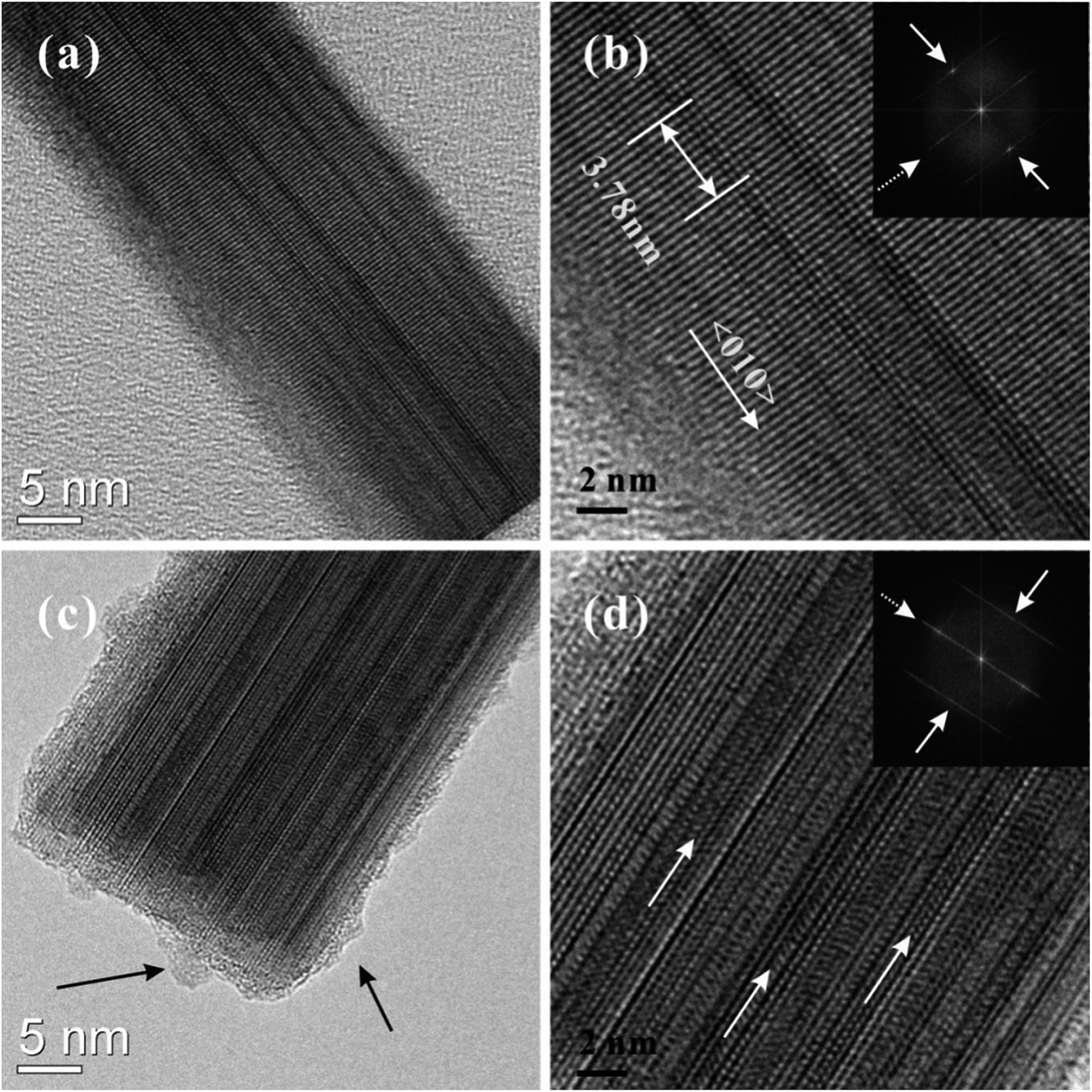 | ||
| Fig. 3 TEM images of as-grown (a–b) and irradiated (c–d) W18O49 nanowires with an irradiation dose of 3.6 × 10¹⁵ phs cm−2. | ||
Second, the lattice atoms of the as-grown W18O49 nanowires were in alignment (Fig. 3(b)). The distance between adjacent crystalline planes along the growth direction was 0.378 nm, which was indexed to be the (010) plane of the monoclinic W18O49 phase. The inset in Fig. 3(b) is the corresponding fast Fourier transform (FFT) image. Two obvious FFT spots indexed to (010) and (0![[1 with combining macron]](https://www.rsc.org/images/entities/char_0031_0304.gif) 0) planes were observed, which indicated that their crystallinity was good. Additionally, there were streaking lines in the FFT image, which were normal to the growth direction of the nanowires, as indicated by the white arrow in the inset of Fig. 3(b). The present streaking lines can be attributed to planar defects such as ordering of oxygen vacancy planes.18,33 After X-ray irradiation, the degree of the W18O49 nanowire lattice orientation decreased. The crystalline lattice slipped along the growth direction of the nanowire, as pointed out by the white arrow in Fig. 3(d). In addition, FFT spots disappeared from the FFT image for irradiated W18O49 nanowires (inset of Fig. 3(d)), which meant that the crystallinity of W18O49 nanowires decreased after X-ray irradiation.
0) planes were observed, which indicated that their crystallinity was good. Additionally, there were streaking lines in the FFT image, which were normal to the growth direction of the nanowires, as indicated by the white arrow in the inset of Fig. 3(b). The present streaking lines can be attributed to planar defects such as ordering of oxygen vacancy planes.18,33 After X-ray irradiation, the degree of the W18O49 nanowire lattice orientation decreased. The crystalline lattice slipped along the growth direction of the nanowire, as pointed out by the white arrow in Fig. 3(d). In addition, FFT spots disappeared from the FFT image for irradiated W18O49 nanowires (inset of Fig. 3(d)), which meant that the crystallinity of W18O49 nanowires decreased after X-ray irradiation.
The chemical composition of W18O49 nanowires before and after X-ray irradiation was characterized, and the results are shown in Fig. 4. In addition to the peaks of C, O, and W, the peak of N at 400 eV was also observed both in as-grown and irradiated W18O49 nanowires (Fig. 4(a)), which indicates that N existed in as-grown W18O49 nanowires. The content of each element is summarized in Table 1. The chemical composition of W18O49 nanowires changed after X-ray irradiation. First, the content of C decreased from 35.27% to 28.46% with increasing X-ray irradiation dose up to 3.6 × 10¹⁵ phs cm−2. It is known that C usually originates from surface-adsorbed carbon, and high-dose X-ray irradiation will cause the temperature of W18O49 nanowires to increase. The decrease in C content may be attributed to surface carbon desorption of W18O49 nanowires at elevated temperature. Second, the content of N in W18O49 nanowires showed a slight increase after X-ray irradiation. Similar results have been also observed for X-ray irradiation experiments on α-Fe2O3 nanoflakes in our previous report.31 The incorporation of N into nanowires was attributed to N atom diffusion at elevated temperatures caused by high-flux X-ray irradiation.
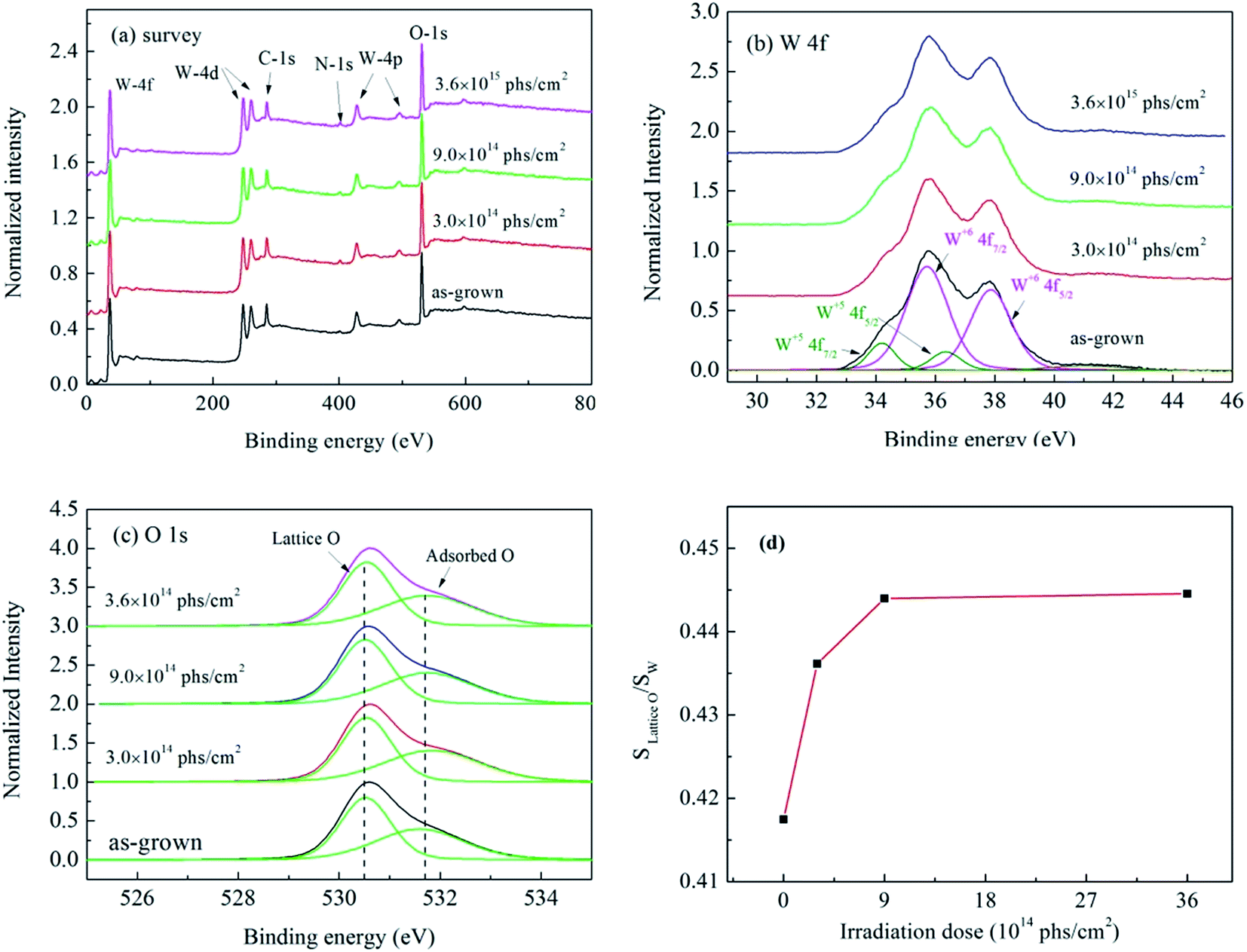 | ||
| Fig. 4 XPS spectra obtained from as-grown and irradiated W18O49 nanowires: (a) survey spectra, (b) W 4f spectra, (c) O 1s spectra, and (d) ratio of lattice O 1s peak area to W 4f area. | ||
| Irradiation dose (phs cm−2) | Element (at%) | S(lattice O)![[thin space (1/6-em)]](https://www.rsc.org/images/entities/char_2009.gif) :SW :SW |
|||
|---|---|---|---|---|---|
| C | N | O | W | ||
| 0 | 35.27 | 3.67 | 47.97 | 13.10 | 0.417 |
| 3.0 × 10¹⁴ | 33.58 | 4.27 | 49.99 | 12.16 | 0.436 |
| 9.0 × 10¹⁴ | 29.89 | 3.47 | 50.54 | 12.82 | 0.444 |
| 3.6 × 10¹⁵ | 28.46 | 5.02 | 51.22 | 13.01 | 0.445 |
Fig. 4(b) shows the W 4f region of the XPS spectrum. From the fitting results, four peaks of W 4f and one peak of W 5p can be seen in the XPS spectrum. The two peaks observed at 35.72 and 37.87 eV correspond to the valence of W6+, and the two peaks observed at 34.20 and 36.35 eV correspond to the valence of W5+.34 Because the XPS spectra of W 4f for as-grown and irradiated nanowires were almost the same, we can conclude that the valence state of W in the nanowire remained unchanged after X-ray irradiation.
Fig. 4(c) shows the O 1s region of the XPS spectrum. The O 1s peak is asymmetric and can be fitted into two peaks located at 530.0 and 531.6 eV, respectively. The peak at approximately 530.5 eV is from the lattice oxygen in the W18O49 crystal (i.e., O–W bonds), whereas the peak at approximately 531.6 eV is from chemisorbed oxygen caused by surface hydroxyls (O–H bonds).29 Comparing the O 1s spectrum before and after X-ray irradiation, it can be seen that more hydroxyls were adsorbed on the surface of W18O49 nanowires after X-ray irradiation. Based on the fitting result of XPS W 4f and O 1s spectra, the ratio of the lattice O 1s area to the W 4f area has been calculated, and the results are shown in Fig. 4(d). The value of Slattice O/SW first increased from 0.417 to 0.444 with an irradiation dose of 9.0 × 10¹⁴ phs cm−2 and then gradually saturated to 0.445 as the irradiation dose increased to 3.6 × 10¹⁵ phs cm−2, which indicated that the lattice oxygen content of W18O49 nanowires increased after X-ray irradiation.
In summary, we observed that more oxygen was incorporated into W18O49 nanowires and crystalline slipping appeared along the growth direction of nanowires after high-energy X-ray irradiation. Fig. 5 shows the diagram of the increase in oxygen content and crystalline slipping caused by X-ray irradiation. W18O49 is an n-type semiconductor because of oxygen vacancies, and the crystalline structure diagram of W18O49 nanowires before X-ray irradiation is shown in Fig. 5(a). We propose two possible processes that may account for the phenomena reported in this study. First, during the X-ray irradiation process, the residual oxygen gas can absorb high-energy X-rays. Because of the high energy of X-rays, O–O bond may be broken and split into O atoms. Second, the nanostructure may absorb X-rays and the temperature of the sample may increase. Especially considering the small size of the nanowires, the heat dissipation will be limited, and the local temperature is expected to rise to a very high level. Under such circumstances, O atoms first adsorb on the surface and then diffuse into the W18O49 nanowire lattice as a result of the high temperature. Because a large amount of oxygen vacancies exist in the W18O49 nanowires, O atoms are prone to occupy the oxygen vacancies, as shown in Fig. 5(b). In another side, a large amount of electrons in the valence band of W18O49 nanowires will escape from the surface of nanowires when irradiated by high-flux X-rays. W18O49 is a semiconductor; large amount of electrons may not be supplied in a timely fashion from substrate to make up for the loss of photoelectrons in the valence band, which means the O–W bond will be broken. Therefore, the crystalline structure of W18O49 nanowires was unstable and can easily change under high-flux X-ray irradiation. Compared with a perfect crystalline structure, a crystalline structure with lattice defects has poorer stability. Based on the TEM results, planar defects such as ordering of oxygen vacancy planes were observed from as-grown W18O49 nanowires. The change in crystallinity of W18O49 nanowires is prone to occur along the direction paralleling the ordering of oxygen vacancy planes. Therefore, crystalline slipping was observed along the nanowire growth direction after X-ray irradiation, as shown in Fig. 5(c).
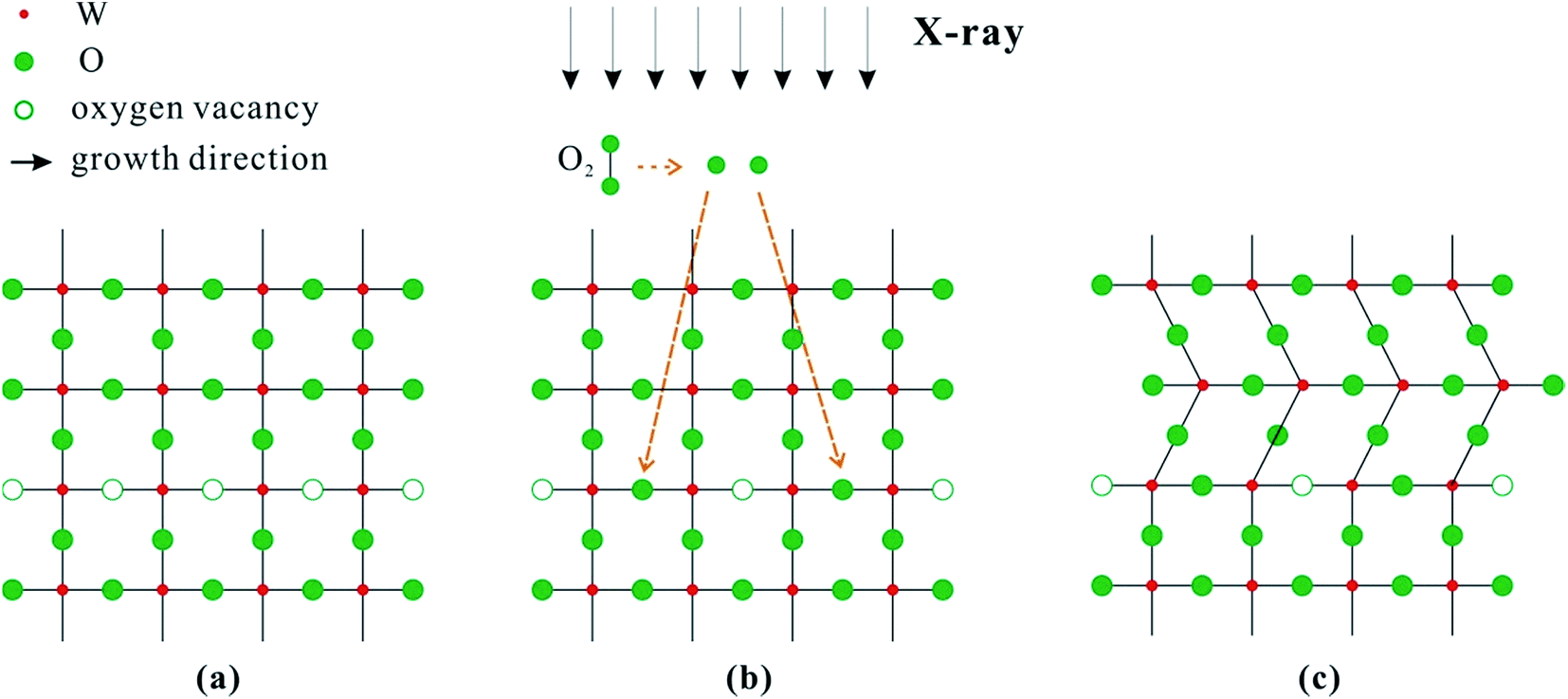 | ||
| Fig. 5 Schematic showing the process of increasing oxygen content and crystalline slipping induced by X-ray irradiation: (a) before X-ray irradiation, (b) during X-ray irradiation, and (c) after X-ray irradiation. | ||
B. Field emission properties of W18O49 nanowires before and after X-ray irradiation
Fig. 6(a) shows the field emission current density versus applied electric field (J–E) characteristics of as-grown and irradiated W18O49 nanowires. The inset shows the corresponding F–N plots. They show straight line except for the high current region, which indicates that the field emission behavior of the prepared W18O49 nanowires follows the F–N mechanism. The nonlinearity at high current could be attributed to the space charge effect.35 The turn-on field (Eturn-on) is defined as the value of the applied field required to induce a current density of 10 μA cm−2, and the threshold field (Ethreshold) refers to the value of the applied field required to induce a current density of 1 mA cm−2. The variation of Ethreshold with X-ray irradiation dose is plotted in Fig. 6(b), and the detailed values are summarized in Table 2. The Ethreshold for W18O49 nanowires first increased from 6.4 to 7.7 and 8.5 MV m−1 after X-ray irradiation with doses of 3.0 × 10¹⁴ and 9.0 × 10¹⁴ phs cm−2, respectively. Then, the Ethreshold decreased to 7.9 MV m−1 when the irradiation dose increased to 3.6 × 10¹⁵ phs cm−2, a value that was still higher than that of as-grown W18O49 nanowires. This result means that the field emission performance of W18O49 nanowires became worse after X-ray irradiation.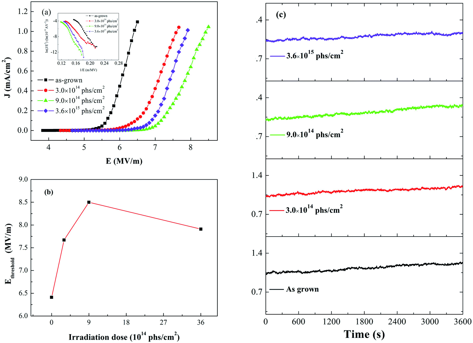 | ||
| Fig. 6 (a) Field emission J–E curves, (b) threshold field and (c) field emission current stability of as-grown and irradiated W18O49 nanowires. | ||
| Irradiation dose (phs cm−2) | Eturn-on (MV m−1) | Ethreshold (MV m−1) | Jmax (mA cm−2) | σ (%) |
|---|---|---|---|---|
| 0 | 5.3 | 6.4 | 10.0 | 5.3 |
| 3.0 × 10¹⁴ | 5.8 | 7.7 | 11.0 | 4.1 |
| 9.0 × 10¹⁴ | 6.8 | 8.5 | 9.5 | 6.9 |
| 3.6 × 10¹⁵ | 6.3 | 7.9 | 10.3 | 4.2 |
The maximum current density (Jmax) for both as-grown and irradiated W18O49 nanowires was measured; this value corresponds to the maximum current density before breakdown occurs. High current density (approximately 10 mA cm−2) can be obtained for as-grown and irradiated W18O49 nanowires (Table 2). No obvious degradation of the maximum current density was observed after X-ray irradiation. The field emission stabilities of as-grown and irradiated W18O49 nanowires were also tested, and the results are shown in Fig. 6(c). The emission current density gradually increased with time, and no degradation was found for either as-grown or irradiated W18O49 nanowires. The emission current density fluctuations (δ) of as-grown and irradiated W18O49 nanowires were calculated, and the results are summarized in Table 2. The emission current fluctuations (δ) were in the range of 4–7% and no obvious relationship with irradiation dose was found. The field emission measurements indicated that after X-ray irradiation, a stable and high current emission still could be obtained from the W18O49 nanowires, with only a slight increase in the threshold field.
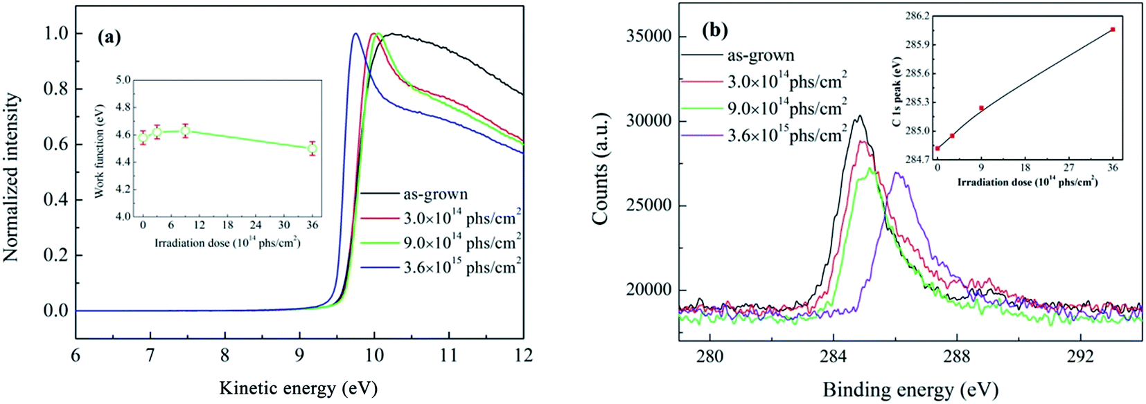
Based on field emission theory, the work functions of field emitters play an important role in field electron emission. Therefore, the work functions of as-grown and irradiated W18O49 nanowires were measured by X-ray photoelectron spectroscopy, and the results are shown in Fig. 7(a). The work function can be calculated using the low kinetic energy cut-off. The inset of Fig. 7(a) shows the obtained work function. The work function values were almost the same (4.60 ± 0.05 eV) for as-grown and irradiated nanowires, except for W18O49 nanowires irradiated with a dose of 3.6 × 10¹⁵ phs cm−2 (4.50 ± 0.05 eV). Obviously, the threshold field increase for W18O49 nanowires after X-ray irradiation was not caused by a change in work function.
 | ||
| Fig. 7 (a) X-ray photoelectron spectroscopy of as-grown and irradiated W18O49 nanowires; inset shows the obtained work function. (b) C 1s spectra obtained from as-grown and irradiated W18O49 nanowires without calibration. The inset shows the plot of C 1s peak versus X-ray irradiation dose. | ||
Fig. 7(b) shows the C 1s region of the XPS spectra of as-grown and irradiated W18O49 nanowires without calibration. The intensity of the C 1s peak declined after X-ray irradiation, which means that the content of surface-adsorbed carbon decreased. At the same time, a shift in the C 1s peak to higher binding energy was also observed after X-ray irradiation, and the degree of the shift in the C 1s peak was proportional to the X-ray irradiation dose (inset of Fig. 7(b)). The shift in the C 1s peak to higher binding energy is usually attributed to charging effects induced by the poor electrical conductivity of a sample.36 During the process of XPS measurement, photoelectrons can escape from the sample surface, and a positive space charge can appear on the surface. If the electrical conductivity of the sample is poor, the electrons cannot be supplied in a timely fashion from the substrate to neutralize the positive space charge. This gives rise to the accumulation of positive charge on the sample surface, which is called the charging effect. Positive charges build a surface potential (Vs) on a sample, which will hinder electrons from escaping from the sample.
When considering the charging effect, the energy equation of the photoelectric effect can be written in the following form:
| Ek = hv − Eb − ϕs − eVs | (1) |
Based on the above discussion, the shift in the C 1s peak to higher binding energy can be attributed to the charging effect induced by poor electrical conductivity of the sample. In our experiment, the C 1s peak shifted to higher binding energy after X-ray irradiation, which indicates that the electrical conductivity of W18O49 nanowires decreased after X-ray irradiation. The decrease in the electrical conductivity of the W18O49 nanowires may contribute to the increase in lattice oxygen content and crystalline slipping. First, W18O49 is an n-type semiconductor because of oxygen vacancies, so an increase in lattice oxygen content means the amount of oxygen vacancies decreases and the electron concentration of the conduction band decreases. Second, crystalline slipping causes the degree of disorder of the lattice structure to rise and the scattering probability for electrons in the transport process to increase, which leads to a decrease in electron mobility. This decrease in electron mobility and electron concentration will cause the electrical conductivity of W18O49 nanowires to become poor.
The field emission performance of a semiconductor material has a close relationship with its electrical conductivity. ZnO nanostructures with higher conductivity have better field emission performance, including lower turn-on and threshold fields. This is because they have a better supply of electrons to the emitting surface.37 Therefore, we suggest that the increase in threshold field was attributed to the decrease in the electrical conductivity of W18O49 nanowires after X-ray irradiation, which was induced by crystalline defects and decrease in the amount of oxygen vacancy. Early studies have shown that defects or vacancies would have effects on the field emission properties of low-dimensional nanomaterials.38,39 Oxygen vacancy is the main defect affecting the electronics properties of metal oxide nanomaterials. Oxygen vacancy will form a donor state claimed as an impurity energy state in metal oxide nanomaterials, such as in ZnO nanostructures. It results in the increasing of electron concentration in the conduction band40 and shifting of Fermi level toward vacuum, which increase the field emission current.38,39 Our results agree with the above findings.
We also note that the threshold field of W18O49 nanowires then decreased to 7.9 MV m−1 when the irradiation dose increased to 3.6 × 10¹⁵ phs cm−2. This may be due to nanoscale protuberances that appear on the surface of W18O49 nanowires after high-dose X-ray irradiation. Nanoscale protuberances reduce the diameter of the field emitter and thereby increase the field enhancement, which will enhance electron field emission.26,41 Therefore, the decrease in the threshold field of the W18O49 nanowires was observed when the irradiation dose increased to 3.6 × 10¹⁵ phs cm−2.
4. Conclusions
High-energy X-ray irradiation will change the crystalline structure, chemical composition, and field emission performance of W18O49 nanowires. After X-ray irradiation, nanoscale protrusions on the surface and crystalline slipping were observed for W18O49 nanowires. The content of lattice oxygen increased and more nitrogen was incorporated into W18O49 nanowires after X-ray irradiation. Nevertheless, a stable and high current emission can be obtained from W18O49 nanowires after X-ray irradiation, with a slight increase in the threshold field. This increase in the threshold field was attributed to the decrease in the electrical conductivity of W18O49 nanowires induced by increasing lattice oxygen content and crystalline defects.Conflicts of interest
There are no conflicts to declare.Acknowledgements
The authors gratefully acknowledge financial support from the National Key Research and Development Program of China (Grant No. 2016YFA0202001), the National Key Basic Research Program of China (Grant No. 2010CB327703), the Science and Technology Department of Guangdong Province, the Fundamental Research Funds for the Central Universities, and the Guangzhou Science Technology and Innovation Commission (Grant No. 201504010024).References
- N. S. Xu and S. E. Huq, Mater. Sci. Eng., R, 2005, 48, 47 CrossRef.
- S. S. Fan, M. G. Chapline, N. R. Franklin, T. W. Tombler, A. M. Cassell and H. J. Dai, Science, 1999, 283, 512 CrossRef CAS PubMed.
- W. B. Choi, D. S. Chung, J. H. Kang, H. Y. Kim, Y. W. Jin, I. T. Han, Y. H. Lee, J. E. Jung, N. S. Lee, G. S. Park and J. M. Kim, Appl. Phys. Lett., 1999, 75, 3129 CrossRef CAS.
- C. J. Lee, T. J. Lee, S. C. Lyu, Y. Zhang, H. Ruh and H. J. Lee, Appl. Phys. Lett., 2002, 81, 3648 CrossRef CAS.
- S. H. Luo, Q. Wan, W. L. Liu, M. Zhang, Z. F. Di, S. Y. Wang, Z. T. Song, C. L. Lin and J. Y. Dai, Nanotechnology, 2004, 15, 1424 CrossRef CAS.
- Y. W. Zhu, T. Yu, F. C. Cheong, X. J. Xui, C. T. Lim, V. B. C. Tan, J. T. L. Thong and C. H. Sow, Nanotechnology, 2005, 16, 88 CrossRef CAS.
- B. D. Liu, Y. Bando, C. C. Tang, F. F. Xu and D. Golberg, J. Phys. Chem. B, 2005, 109, 21521 CrossRef CAS PubMed.
- D. J. Late, R. V. Kashid, C. S. Rout, M. A. More and D. S. Joag, Appl. Phys. A, 2010, 98, 751 CrossRef CAS.
- H. D. Zheng, J. Z. Ou, M. S. Strano, R. B. Kaner, A. Mitchell and K. Kalantar-Zadeh, Adv. Funct. Mater., 2011, 21, 2175 CrossRef CAS.
- L. F. Zhu, J. C. She, J. Y. Luo, S. Z. Deng, J. Chen and N. S. Xu, J. Phys. Chem. C, 2010, 114, 15504 CAS.
- M. R. Waller, T. K. Townsend, J. Zhao, E. M. Sabio, R. L. Chamousis, N. D. Browning and F. E. Osterloh, Chem. Mater., 2012, 24, 698 CrossRef CAS.
- H. J. Chen, N. S. Xu, S. Z. Deng, D. Y. Lu, Z. L. Li, J. Zhou and J. Chen, Nanotechnology, 2007, 18, 205701 CrossRef.
- H. D. Zheng, Y. Tachibana and K. Kalantar-zadeh, Langmuir, 2010, 26, 19148 CrossRef CAS PubMed.
- G. Gu, B. Zheng, W. Q. Han, S. Roth and J. Liu, Nano Lett., 2002, 2, 849 CrossRef CAS.
- J. Thangala, S. Vaddiraju, R. Bogale, R. Thurman, T. Powers, B. Deb and M. K. Sunkara, Small, 2007, 3, 890 CrossRef CAS PubMed.
- Y. Baek and K. Yong, J. Phys. Chem. C, 2007, 111, 1213 CAS.
- K. Lee, W. S. Seo and J. T. Park, J. Am. Chem. Soc., 2003, 125, 3408 CrossRef CAS PubMed.
- J. Zhou, Y. Ding, S. Z. Deng, L. Gong, N. S. Xu and Z. L. Wang, Adv. Mater., 2005, 17, 2107 CrossRef CAS.
- Y. Li, Y. Bando and D. Gelberg, Adv. Mater., 2003, 15, 1294 CrossRef CAS.
- J. Zhou, L. Gong, S. Z. Deng, J. Chen, J. C. She and N. S. Xu, Appl. Phys. Lett., 2005, 87, 223108 CrossRef.
- X. H. Zhang, L. Gong, K. Liu, Y. Z. Cao, X. Xiao, W. M. Sun, X. J. Hu, Y. H. Gao, J. A. Chen, J. Zhou and Z. L. Wang, Adv. Mater., 2010, 22, 5292 CrossRef CAS PubMed.
- L. Li, Y. Zhang, X. S. Fang, T. Y. Zhai, M. Y. Liao, X. L. Sun, Y. Koide, Y. Bando and D. Golberg, J. Mater. Chem., 2011, 21, 6525 RSC.
- J. Chen, Y. Y. Dai, J. Luo, Z. L. Li, S. Z. Deng, J. C. She and N. S. Xu, Appl. Phys. Lett., 2007, 90, 253105 CrossRef.
- J. G. Liu, Z. J. Zhang, Y. Zhao, X. Su, S. Liu and E. G. Wang, Small, 2005, 1, 310 CrossRef CAS PubMed.
- Z. L. Li, F. Liu, N. S. Xu, J. Chen and S. Z. Deng, J. Vac. Sci. Technol., B: Microelectron. Nanometer Struct.--Process., Meas., Phenom., 2009, 27, 2420 CrossRef CAS.
- F. Liu, T. Y. Guo, Z. Xu, H. B. Gan, L. F. Li, J. Chen, S. Z. Deng, N. S. Xu, D. Golberg and Y. Bando, J. Mater. Chem. C, 2013, 1, 3217 RSC.
- W. Q. Chen, C. X. Zhao, J. Q. Wu, S. Z. Deng, N. S. Xu and J. Chen, Appl. Phys. Lett., 2013, 103, 141915 CrossRef.
- W. Q. Chen, R. Z. Zhan, S. Z. Deng, N. S. Xu and J. Chen, J. Appl. Phys., 2014, 116, 133506 CrossRef.
- C. X. Zhao, S. Z. Deng, N. S. Xu and J. Chen, RSC Adv., 2015, 5, 70059 RSC.
- J. Q. Wu, B. Wang, F. T. Yi, S. Z. Deng, N. S. Xu and J. Chen, J. Appl. Phys., 2013, 114, 184306 CrossRef.
- J. Q. Wu, Y. Zhang, B. Wang, F. T. Yi, S. Z. Deng, N. S. Xu and J. Chen, Nucl. Instrum. Methods Phys. Res., Sect. B, 2013, 304, 49 CrossRef CAS.
- C. X. Zhao, Y. F. Li, Y. C. Chen, J. Q. Wu, B. Wang, F. T. Yi, S. Z. Deng, N. S. Xu and J. Chen, Nanotechnology, 2013, 24, 275703 CrossRef CAS PubMed.
- J. Thangala, Z. Q. Chen, A. Chin, C. Z. Ning and M. K. Sunkara, Cryst. Growth Des., 2009, 9, 3177 CAS.
- J. Y. Luo, F. L. Zhao, L. Gong, H. J. Chen, J. Zhou, Z. L. Li, S. Z. Deng and N. S. Xu, Appl. Phys. Lett., 2008, 92, 093124 CrossRef.
- Y. Chen, S. Z. Deng, N. S. Xu, J. Chen, X. C. Ma and E. G. Wang, Mater. Sci. Eng., A, 2002, 327, 16 CrossRef.
- J. A. C. Santana, Quantitative Core Level Photoelectron Spectroscopy, Morgan & Claypool Publishers, 2015, ch. 4 Search PubMed.
- J. C. She, Z. M. Xiao, Y. H. Yang, S. Z. Deng, J. Chen, G. W. Yang and N. S. Xu, ACS Nano, 2008, 2, 2015 CrossRef CAS PubMed.
- K. K. Naik, R. Khare, D. Chakravarty, M. A. More, R. Thapa, D. J. Late and C. S. Rout, Appl. Phys. Lett., 2014, 105, 233101 CrossRef.
- A. Z. Liao, J. B. Chen, C. W. Wang, X. F. Su, Y. Li and J. Wang, J. Vac. Sci. Technol., B: Microelectron. Nanometer Struct.--Process., Meas., Phenom., 2016, 34, 021803 Search PubMed.
- A. Kolmakov, Y. X. Zhang, G. S. Cheng and M. Moskovits, Adv. Mater., 2003, 15, 997 CrossRef CAS.
- Z. Zheng, L. Liao, B. Yan, J. X. Zhang, H. Gong, Z. X. Shen and T. Yu, Nanoscale Res. Lett., 2009, 4, 1115 CrossRef CAS PubMed.
| This journal is © The Royal Society of Chemistry 2018 |