DOI:
10.1039/C7RA12642E
(Paper)
RSC Adv., 2018,
8, 8349-8354
Dual role of Ag nanowires in ZnO quantum dot/Ag nanowire hybrid channel photo thin film transistors†
Received
21st November 2017
, Accepted 13th February 2018
First published on 22nd February 2018
Abstract
High mobility and p-type thin film transistors (TFTs) are in urgent need for high-speed electronic devices. In this work, ZnO quantum dot (QD)/Ag nanowire (NW) channel TFTs were fabricated by a solution processed method. The Ag NWs play the dual role of dopant and providing the charge transfer route, which make the channel p-type and enhance its mobility, respectively. The best sample yields an on/off ratio (Ion/Ioff) of 5.04 × 10⁵, a threshold voltage (VT) of 0.73 V, a high field effect mobility (μFE) of 8.69 cm2 V−1 s−1, and a subthreshold swing (SS) of 0.41 V dec−1. Owing to the strong ultraviolet (UV) absorption and photo-induced carrier separation ability of ZnO QDs and the fast carrier transport of Ag NWs, the devices acquire a high external quantum efficiency (EQE) and ultra-fast response under 365 nm UV illumination. The UV-modulated ZnO QD/Ag NW hybrid channel photo TFTs have potential for future application in optoelectronic devices, such as photodetectors and photoswitches.
Introduction
Thin film transistors (TFTs) based on metal oxide semiconductors are a key constituent for numerous optoelectronic devices such as sensors and displays. High mobility p-type TFTs are in urgent need for complementary metal oxide semiconductor (CMOS) technology. Wide-band gap metal oxide semiconductors, such as zinc oxide (ZnO),1 zinc-indium-tin oxide (ZITO),2 and indium-gallium-zinc oxide (IGZO)3 have been widely studied for TFTs. ZnO, owing to its abundance, low price, and being indium free, has great potential in the application of TFTs. Various dopants, such as H,4 Li,5 Na,6 Ca,7 B,8 Al,9 and Ti10 have been utilized to acquire better electrical performance. However, most research is focused on n-type TFTs. p-Type TFTs materials are limited to NiO,11–13 SnO,14–19 and CuxO.20–23 There is rarely a report about ZnO-based p-type TFTs due to the difficulty of p-type doping in ZnO.
Recent great progress in light emitting diode (LED) attracts the attention in quantum dots (QDs).24 Quantum confinement effect makes QDs be considered as promising material for the optoelectronic devices. Thus, ZnO QDs with the appropriate band gap may be utilized in ultraviolet (UV)-related photo transistors. Compared with RF magnetron sputtering, pulsed laser deposition, and atomic layer deposition, solution-processed colloid ZnO QDs can be synthesized at low-temperature to fulfill the progressive demands for low-cost devices. For one-dimensional nano-material, nanowires (NWs) have been widely studied due to the transport of carriers confined in one dimension. Recently, Zou25 and Park26 fabricated NWs and nanorods (NRs) thin film transistors and acquired high filed effect mobility (μFE) owing to this property. The μFE are 110 cm2 V−1 s−1 for In2O3 single NW TFTs and 1.77 cm2 V−1 s−1 for ZnO NRs TFTs, respectively. The composite material combined with nanoscale components is the foremost scientific research now, which can take full advantage of these constituents. There were some reports about hybrid channel of ZnO and graphene with UV response.27–30 Herein, we employ the Ag NWs utilizing its good conductivity to improve hybrid channel mobility. Besides, Ag is doped into ZnO QDs by annealing, which realizes the ZnO based p-type TFTs. With strong light absorption and photo-induced carriers separation ability of ZnO QDs and fast carrier transport of Ag NWs, it is expected to fabricate these hybrid channel TFTs for the future photo-modulate transistors.
Experimental
Synthesis of colloid ZnO QDs
Colloid ZnO QDs were synthesized by the previous method with some modification.24 In a typical reaction, 3 mmol zinc acetate hydrate and 30 mL dimethyl sulphoxide (DMSO) are loaded in a flask with magnetic stirring under ambient conditions. After zinc acetate being completely dissolved, 10 mL ethanol solution of 5.5 mmol tetramethylammonium hydroxide (TMAH) is added slowly. The reaction is proceeded for 2 h. The obtained stock was divided into 8 parts. Each part is precipitated by adding 5 mL ethyl acetate. After centrifugation, each one is redispersed in 2 mL ethanol with additional ligands of 30 μL 2-ethanolamine to stabilize the nanoparticles. The ZnO QDs are further washed with ethyl acetate and redispersed in 4 mL ethanol. The solution is filtered by 0.22 μL PTFE filter before use. The details of characterization of ZnO QDs are presented in the electronic ESI.†
Devices fabrication
Fig. 1a shows the fabrication process and framework of device. The channel is deposited on the p++ Si/300 nm SiO2 of (100) orientation substrate. The wafers were purchased from University Wafer and cleaned in ultrasonic baths of acetone, ethanol and deionized water for 10 min, respectively, followed by drying with N2 gas and oxide plasma treatment before used. Then, the Ag NWs film is grown by dip-coating technic. Ag NWs dispersed in ethanol were purchased from Jinan Shangke New Material Co., Ltd. The average length and width of Ag NWs are 60 μm and 80 nm, respectively. The concentration of Ag NWs is diluted to 0.1 mg mL−1 and the lifting speed of substrate is 10 μm s−1. The NWs would self-assemble aligned owing to the surface tension and solvent evaporation. ZnO QDs were then spin-coated on the NWs film at 3000 rpm. for 35 s, twice. Subsequently, ambient annealing process at different temperature was carried out for 1 h. 100 nm thick Al electrodes were finally evaporated by electron beam evaporation technology with shadow mask as source and drain. The channel width and length were 1000 and 200 μm, respectively.
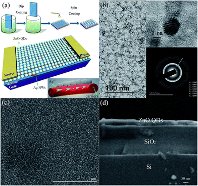 |
| | Fig. 1 (a) The schematic diagram of the TFT structure. (b) TEM image and HRTEM image of the ZnO QDs. (c) The surface SEM image of TFT. (d) The cross-section SEM image of TFT. | |
Characterization
Size and morphologies of ZnO QDs were characterized by high-resolution transmission electron microscopy (HRTEM, JEM-2100). The arrangement of Ag NWs, surface morphologies and cross-section of ZnO QDs film were observed by field-emission scanning electron microscopy (FE-SEM Hitachi S-4800). X-ray photoelectron spectroscopy with a monochromatic Al-Kα (1486.6 eV) X-ray source (XPS, Thermo ESCALAB 250) measurements were performed to investigate whether Ag was doped into ZnO QDs after annealing. The performances of TFTs were tested with a semiconductor parameter analyzer (Agilent E5270B). The temporal response of UV was examined with a UVA-LED (365 nm).
Results and discussion
Characterization of hybrid channel
Fig. 1b shows the TEM image of ZnO QDs, and the inserts are HRTEM images. The diameters of ZnO QDs are 4 nm on average. The diffraction rings correspond to the X-ray diffraction (XRD) pattern in the Fig. S2 in the ESI,† which confirms the formation of ZnO phase. Fig. 1c and d are the surface and cross-section SEM images of TFT, respectively. Fig. 1c indicates that the spin-coated ZnO QDs film on the Ag NWs is smooth and flat. And the ZnO QDs film has a thickness of about 50 nm as shown in Fig. 1d.
To investigate the performance of TFTs and reveal the carrier transport of different morphological feature of Ag NWs, the TFTs are annealed at 100, 150, 200, and 300 °C, respectively. From Fig. 2, Ag NWs keep the NW shape under 100 and 150 °C, while melt into particles under 200 and 300 °C. However, ZnO QDs barely have change from the SEM images (the insert graph in Fig. 2).
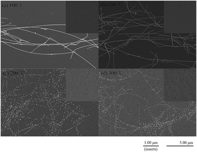 |
| | Fig. 2 The SEM images of Ag NWs at different annealing temperature (a) 100 °C, (b) 150 °C, (c) 200 °C, (d) 300 °C. Inserts are the corresponding surface of ZnO QDs film. | |
To clarify whether Ag was doped into ZnO QDs, XPS measurement was conducted on the sample annealed at 100 °C. Fig. 3a depicts the full spectrum of the sample. C 1s at Eb = 284.8 eV is used to the calibration element from the XPS instrument itself. Considering that Ag peak can be hardly observed from full spectrum, high-resolution spectra of Ag, Zn and O are shown in the Fig. 3b–d, respectively. In Fig. 3b, the peaks at binding energy of 367.25 eV and 373.15 eV ascribe to Ag 3d5/2 and 3d3/2 belonging to the monovalent Ag. There is no zerovalent Ag peak for bulk Ag (368.2 eV of 3d5/2 and 374.2 eV of 3d3/2),31 which illustrates that the XPS measurements did not observe the Ag NWs. Due to the contact of Ag NWs and ZnO QDs, the Fermi levels of two components equilibrate. Some of the free electrons of Ag NWs transfer to the vacant conduction band (CB) of ZnO QDs at the interfaces of ZnO/Ag, resulting in the monovalent Ag and the p-type ZnO QDs thin film. The peaks centered at 1021 and 1044 eV in the Fig. 3c are attributed to the Zn 2p3/2 and 2p1/2, which confirms that Zn exists in divalent states. In Fig. 3d, the O 1s profile can be fitted into three Gaussian distributions representing the different oxygen state. The OI, OII, and OIII belong to the lattice oxygen, oxygen vacancy, and oxygen bonds in the hydroxide, which located at 530.25 eV, 531.50 eV and 532.30 eV, respectively.32
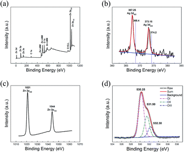 |
| | Fig. 3 (a) Complete XPS spectrum of ZnO QDs/Ag NWs hybrid channel annealed at 100 °C. High-resolution spectra of the sample for the elements of (b) Ag, (c) Zn, and (d) O. | |
Devices performance
Fig. 4 shows the transfer characteristics of 4 samples of different annealing temperature under dark and 365 nm UV illumination. As Ag doped into ZnO QDs film investigated by XPS measurements, Fig. 4a–d show p-type transfer characteristic. The electrical parameters, threshold voltage (VT), μFE and subthreshold swing (SS), are also listed in each figure. The μFE is calculated by the following eqn (1):| |
 | (1) |
where IDS, VGS, VDS and Ci are the drain–source current, gate–source voltage, drain–source voltage and the capacitance per unit area of the gate insulator (0.0115 μF cm−2), repectively. The SS, another key parameter to indicate the interface defects, is calculated by the eqn (2):| |
 | (2) |
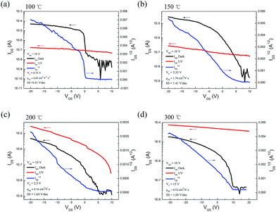 |
| | Fig. 4 The transfer characteristics of TFTs under dark and UV illumination at different annealing temperature (a) 100 °C, (b) 150 °C, (c) 200 °C, (d) 300 °C. | |
It is observed that the performances of devices annealed at 100 and 150 °C are obviously superior to those at higher annealing temperature. As shown in Fig. 2, the Ag NWs transform to Ag particles under 200 and 300 °C annealing. Due to the existence of Ag NWs, the μFE of devices annealed at 100 and 150 °C are high. The best sample annealed at 100 °C yields an on/off ratio (Ion/Ioff) of 5.04 × 10⁵, a VT of 0.73 V, a μFE of 8.69 cm2 V−1 s−1, and a SS of 0.41 V dec−1. When the devices illuminated by the 365 nm ultraviolet of 80 μW cm−2 intensity (P), the transfer curves change differently. Photo-induced holes and electrons from ZnO QDs enhance the conductivity of channel and break the TFTs switch character. The control by VGS is loose, and IDS is a bit amplified and limited by VGS in the accumulation region and depletion region, respectively. Thus, the curves keep particular slopes. It is deduced that the current goes through the Ag NWs in the NW presence devices, and the current flux is limited by the ultra-thin Ag NWs. While in the NW burnt devices, the current path comes to the wider ZnO QDs film. The changes of transfer characteristic and IDS are like our previous research.33 Electrical parameters of TFTs are summarized in Table 1. The output characteristics of devices under dark and UV illumination are presented in the Fig. S5 and S6 in the ESI,† and the transfer characteristics of ZnO QDs film without Ag NWs is shown in Fig. S7 in the ESI.†
Table 1 Electrical parameters of TFTs with ZnO QDs/Ag NWs hybrid channel
| Sample (at different annealing temp.) |
VT (V) |
μFE (cm2 V−1 s−1) |
SS (V dec−1) |
Ion/Ioff (×105) |
| 100 °C |
0.73 |
8.69 |
0.41 |
5.04 |
| 150 °C |
3.33 |
1.74 |
1.41 |
0.36 |
| 200 °C |
2.5 |
0.16 |
1.64 |
0.39 |
| 300 °C |
15 |
0.52 |
1.26 |
0.09 |
To further reveal the charge transport route, time-resolved UV photocurrent on/off measurements are carried out, as shown in Fig. 5. The inserts are five repeated cycles. VGS was set at 10 V to confine the current at dark (Idark). It can be clearly seen from Fig. 5, the response of 365 nm UV of samples annealed at 100 and 150 °C is much faster than the samples annealed at 200 and 300 °C. The characteristic times for growth (τg) and decay (τd) of the photocurrent are 0.17 and 0.37 s of sample annealed at 100 °C. In Fig. 5a and b, the photo current (Iphoto) generates and rapidly soars to a maximum, while exposed to the ultraviolet. Due to the current crowding effect, the carriers accumulate in the NWs and Iphoto will decrease to a stable value. When the UV light is off, the Iphoto quenches to Idark level. The response of UV is like our previous ZnO NR UV photodetectors.34–36 About samples annealed at 200 and 300 °C, the response is much slow and similar to the ZnO nanoparticles UV photodetector.37 The time-resolved UV response confirms the charge transfer mechanism discussed above.
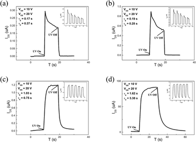 |
| | Fig. 5 The growth and decay of photocurrent of photo transistors at different annealing temperature (a) 100 °C, (b) 150 °C, (c) 200 °C, (d) 300 °C. Inserts are five repeated cycles. | |
Fig. 6 depicts the energy band of surface ZnO QDs and the schematic diagram of charge transfer. As a result of the chemical absorbed O2 on the surface of ZnO QDs without UV light, the oxygen molecules capture free electrons [O2(g) + e− = O2−(ad)], which makes the band of ZnO QDs bend upward and create a low conductivity depletion region on the surface. The effect is particularly prominent in oxide semiconductors, especially in nano structures. Under UV illumination with photon energy higher than the semiconductor band gap, photo-induced hole–electron pairs generate. The photo-generated holes react with the chemisorbed oxygen [h+ + O2−(ad) = O2(g)], resulting in increasing of free carrier concentration in the ZnO QDs and forming the carrier transport route in different situation, as shown in Fig. 6b and d.
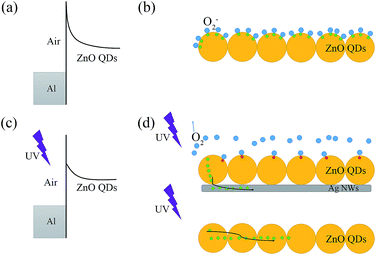 |
| | Fig. 6 The energy band of the surface ZnO QDs under (a) dark and (c) UV illumination, and the schematic diagram of the charge transfer under (b) dark and (d) UV illumination. Red dots = holes, and green dots = electrons. | |
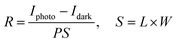
Moreover, some significant UV response parameters are listed in Table 2. The calculated values are all applied at VGS of 10 V and VDS of 20 V. The responsivity (R) is used to indicate the photo-to-current efficiency. It is determined by the eqn (3):
| |
 | (3) |
where
P is the optical signal power density, and
S is the effective photo-electric conversion area, respectively. The device performance can be expressed in terms of another vital parameter, external quantum efficiency (EQE), which is a function of photon flux density and incident photon energy as
eqn (4):
| |
 | (4) |
where
q is the quantity of one electron,
h is the Plank constant, and
ν is the frequency of absorbed photon. Note that the
R and EQE both increase mainly by the
Iphoto in the same condition.
Table 2 UV response parameters of ZnO QDs/Ag NWs hybrid channel TFTs
| Sample (at different annealing temp.) |
τg (s) |
τd (s) |
R (A W−1) |
EQE (%) |
| 100 °C |
0.17 |
0.37 |
0.64 |
218 |
| 150 °C |
0.19 |
0.28 |
2.33 |
793 |
| 200 °C |
1.03 |
0.75 |
6.01 |
2048 |
| 300 °C |
1.62 |
3.38 |
351 |
119![[thin space (1/6-em)]](https://www.rsc.org/images/entities/char_2009.gif) 565 565 |
As discussed in XPS data, as-implanted Ag atoms by annealing occupy almost ideal substitutional Zn sites.38 Ag atoms are incorporated in the form of point defects of AgZn acceptor in 3d10 states, with part of the silver formed with silver oxide.39 The AgZn acceptor actualizes the formation of p-type ZnO. Besides, the heterojunction formed by ZnO QDs and Ag NWs makes the fast response of UV detection. The photo-induced carriers from UV illuminated ZnO are transferred to Ag NWs and transported away rapidly. The dual role of Ag NWs is depicted clearly in Fig. 1a.
Conclusions
In summary, we have fabricated the photo-modulated p-type TFTs with ZnO QDs/Ag NWs hybrid channel, and cleared the charge transfer in the channel under UV illumination. At low annealing temperature of 100 and 150 °C, the Ag NWs firstly provide the Ag dopant and make the thin channel p-type as XPS measurements and TFTs transfer characteristic demonstrated. Moreover, Ag NWs play a role of charge transfer route, which enhances the μFE. The sample annealed at 100 °C yields an on/off ratio (Ion/Ioff) of 5.04 × 10⁵, a VT of 0.73 V, a μFE of 8.69 cm2 V−1 s−1, and a SS of 0.41 V dec−1. In addition, the TFTs show superior response of 365 nm UV illumination due to the surface ZnO QDs. Owing to the strong UV absorption and photo-induced carriers separation ability of ZnO QDs and fast carrier transport of Ag NWs, the devices display the high EQE and ultra-fast response. The sample annealed at 100 °C acquire a 0.17 s of τg, 0.37 s of τd, 0.64 A W−1 of responsivity, and 218% EQE. The UV-modulated ZnO QDs/Ag NWs hybrid channel TFTs have potential for the future application in optoelectronic devices, such as photodetector and photoswitch.
Conflicts of interest
There are no conflicts to declare.
Acknowledgements
This work was supported by National Natural Science Foundation of China under Grant No. 51302244 and 91333203, and Zhejiang Provincial Natural Science Foundation of China under Grant No. LY17E020005.
References
- Y. Y. Lin, C. C. Hsu, M. H. Tseng, J. J. Shyue and F. Y. Tsai, ACS Appl. Mater. Interfaces, 2015, 7, 22610–22617 CAS.
- Q. J. Jiang, J. G. Lu, J. P. Cheng, X. F. Li, R. J. Sun, L. S. Feng, W. Dai, W. C. Yan and Z. Z. Ye, Appl. Phys. Lett., 2014, 105, 132105 CrossRef.
- K. Nomura, H. Ohta, A. Takagi, T. Kamiya, M. Hirano and H. Hosono, Nature, 2004, 432, 488–492 CrossRef CAS PubMed.
- A. Abliz, C. W. Huang, J. Wang, L. Xu, L. Liao, X. Xiao, W. W. Wu, Z. Fan, C. Jiang, J. Li, S. Guo, C. Liu and T. Guo, ACS Appl. Mater. Interfaces, 2016, 8, 7862–7868 CAS.
- S. Y. Park, B. J. Kim, K. Kim, M. S. Kang, K. H. Lim, T. I. Lee, J. M. Myoung, H. K. Baik, J. H. Cho and Y. S. Kim, Adv. Mater., 2012, 24, 834–838 CrossRef CAS PubMed.
- K. Kim, S. Y. Park, K.-H. Lim, C. Shin, J.-M. Myoung and Y. S. Kim, J. Mater. Chem., 2012, 22, 23120 RSC.
- W. Yu, D. Han, G. Cui, Y. Cong, J. Dong, X. Zhang, X. Zhang, Y. Wang and S. Zhang, Jpn. J. Appl. Phys., 2016, 55, 04EK05 CrossRef.
- S. Gandla, S. R. Gollu, R. Sharma, V. Sarangi and D. Gupta, Appl. Phys. Lett., 2015, 107, 152102 CrossRef.
- T. S. Kang, T. Y. Kim, K. S. Yoon, J. M. Kim, H. S. Im and J. P. Hong, J. Mater. Chem. C, 2014, 2, 10209–10216 RSC.
- G. Cui, D. Han, W. Yu, P. Shi, Y. Zhang, L. Huang, Y. Cong, X. Zhou, X. Zhang, S. Zhang, X. Zhang and Y. Wang, Jpn. J. Appl. Phys., 2016, 55, 04EK06 CrossRef.
- A. Liu, G. Liu, H. Zhu, B. Shin, E. Fortunato, R. Martins and F. Shan, Appl. Phys. Lett., 2016, 108, 233506 CrossRef.
- T. Lin, X. Li and J. Jang, Appl. Phys. Lett., 2016, 108, 233503 CrossRef.
- J. Jiang, X. Wang, Q. Zhang, J. Li and X. X. Zhang, Phys. Chem. Chem. Phys., 2013, 15, 6875–6878 RSC.
- R. F. P. Martins, A. Ahnood, N. Correia, L. M. N. P. Pereira, R. Barros, P. M. C. B. Barquinha, R. Costa, I. M. M. Ferreira, A. Nathan and E. E. M. C. Fortunato, Adv. Funct. Mater., 2013, 23, 2153–2161 CrossRef CAS.
- J. A. Caraveo-Frescas, P. K. Nayak, H. A. Al-Jawhari, D. B. Granato, U. Schwingenschlögl and H. N. Alshareef, ACS Nano, 2013, 7, 5160–5167 CrossRef CAS PubMed.
- J. A. Caraveo-Frescas, M. A. Khan and H. N. Alshareef, Sci. Rep., 2014, 4, 5243 CrossRef CAS PubMed.
- Y. S. Li, J. C. He, S. M. Hsu, C. C. Lee, D. Y. Su, F. Y. Tsai and I. C. Cheng, IEEE Electron Device Lett., 2016, 37, 46–49 CrossRef.
- J. H. Lee, Y. J. Choi, C. Y. Jeong, D. K. Jung, S. Ham and H. I. Kwon, IEEE Electron Device Lett., 2016, 37, 295–298 CrossRef CAS.
- P. C. Chen, Y. H. Wu, Z. W. Zheng, Y. C. Chiu, C. H. Cheng, S. S. Yen, H. H. Hsu and C. Y. Chang, J. Disp. Technol., 2016, 12, 224–227 CrossRef CAS.
- A. Dindar, J. B. Kim, C. Fuentes-Hernandez and B. Kippelen, Appl. Phys. Lett., 2011, 99, 172104 CrossRef.
- Z. Q. Yao, S. L. Liu, L. Zhang, B. He, A. Kumar, X. Jiang, W. J. Zhang and G. Shao, Appl. Phys. Lett., 2012, 101, 042114 CrossRef.
- A. Liu, G. Liu, H. Zhu, H. Song, B. Shin, E. Fortunato, R. Martins and F. Shan, Adv. Funct. Mater., 2015, 25, 7180–7188 CrossRef CAS.
- W. Maeng, S.-H. Lee, J.-D. Kwon, J. Park and J.-S. Park, Ceram. Int., 2016, 42, 5517–5522 CrossRef CAS.
- X. Dai, Z. Zhang, Y. Jin, Y. Niu, H. Cao, X. Liang, L. Chen, J. Wang and X. Peng, Nature, 2014, 515, 96–99 CrossRef CAS PubMed.
- X. Zou, X. Liu, C. Wang, Y. Jiang, Y. Wang, X. Xiao and L. Liao, ACS Nano, 2012, 7, 804–810 CrossRef PubMed.
- J. H. Park, J. H. Park, P. Biswas, K. Kwon do, S. W. Han, H. K. Baik and J. M. Myoung, ACS Appl. Mater. Interfaces, 2016, 8, 11564–11574 CAS.
- W. Guo, S. Xu, Z. Wu, N. Wang, M. M. Loy and S. Du, Small, 2013, 9, 3031–3036 CrossRef CAS PubMed.
- V. Q. Dang, T. Q. Trung, D. I. Kim, T. Duy le, B. U. Hwang, D. W. Lee, B. Y. Kim, D. Toan le and N. E. Lee, Small, 2015, 11, 3054–3065 CrossRef CAS PubMed.
- V. Q. Dang, T. Q. Trung, T. Duy le, B. Y. Kim, S. Siddiqui, W. Lee and N. E. Lee, ACS Appl. Mater. Interfaces, 2015, 7, 11032–11040 CAS.
- D. Shao, J. Gao, P. Chow, H. Sun, G. Xin, P. Sharma, J. Lian, N. A. Koratkar and S. Sawyer, Nano Lett., 2015, 15, 3787–3792 CrossRef CAS PubMed.
- L. Duan, B. X. Lin, W. Y. Zhang, S. Zhong and Z. X. Fu, J. Phys. Chem. C, 2012, 116, 16182–16190 Search PubMed.
- Y. Sun, Y. Jiang, H. Peng, J. Wei, S. Zhang and S. Chen, Nanoscale, 2017, 9, 8962–8969 RSC.
- W. Wang, X. Pan, W. Dai, Y. Zeng and Z. Ye, RSC Adv., 2016, 6, 32715–32720 RSC.
- Y. Zeng, X. Pan, W. Dai, Y. Chen and Z. Ye, RSC Adv., 2015, 5, 66738–66741 RSC.
- Y. Zeng, Z. Ye, B. Lu, W. Dai and X. Pan, Appl. Phys. A, 2016, 122, 296 CrossRef.
- Y. Zeng, X. Pan, B. Lu and Z. Ye, RSC Adv., 2016, 6, 31316–31322 RSC.
- Y. Jin, J. Wang, B. Sun, J. C. Blakesley and N. C. Greenham, Nano Lett., 2008, 8, 1649–1653 CrossRef CAS PubMed.
- U. Wahl, E. Rita, J. G. Correia, T. Agne, E. Alves and J. C. Soares, Superlattices Microstruct., 2006, 39, 229–237 CrossRef CAS.
- N. Gruzintsev, V. T. Volkov and E. E. Yakimov, Semiconductors, 2003, 37, 259–262 CrossRef.
Footnote |
| † Electronic supplementary information (ESI) available. See DOI: 10.1039/c7ra12642e |
|
| This journal is © The Royal Society of Chemistry 2018 |
Click here to see how this site uses Cookies. View our privacy policy here. 
 Open Access Article
 This Open Access Article is licensed under a Creative Commons Attribution-Non Commercial 3.0 Unported Licence
 *,
Xiaoli Peng,
Qiaoqi Lu,
Fengzhi Wang,
Wen Dai,
Bin Lu and
Zhizhen Ye
*,
Xiaoli Peng,
Qiaoqi Lu,
Fengzhi Wang,
Wen Dai,
Bin Lu and
Zhizhen Ye