 Open Access Article
Approaching completely continuous centimeter-scale graphene by copolymer-assisted transfer†
Arka Karmakara,
Farah Vandrevala a,
Florian Gollierb,
Mahima Ann Philip‡
a,
Simran Shahia and
Erik Einarsson
a,
Florian Gollierb,
Mahima Ann Philip‡
a,
Simran Shahia and
Erik Einarsson *ab
*ab
aDepartment of Electrical Engineering, University at Buffalo, Buffalo, NY, USA. E-mail: erikeina@buffalo.edu
bDepartment of Materials Design and Innovation, University at Buffalo, Buffalo, NY, USA
First published on 5th January 2018
Abstract
Transferring graphene from copper foil to a target substrate should ideally be a nondestructive process, but cracks, holes, and wrinkles have proved difficult to prevent. Here we report a method in which we use a commercially available copolymer in addition to poly(methylmethacrylate) (PMMA) to obtain 99.8% continuous centimeter-scale transferred graphene. Our findings are based on characterization using Raman spectroscopy, quantitative image analysis, scanning electron microscopy, and terahertz time-domain spectroscopy. Compared to conventional methods, this copolymer-assisted approach not only results in fewer holes, but also effectively eliminates cracks and wrinkles. We attribute this to a more thorough relaxation of the initially deposited PMMA by solvent contained in the thicker copolymer layer. This results in improved contact at the PMMA–graphene interface before removal of the underlying copper substrate.
1 Introduction
Continuous graphene is a necessity for many electrical and optical applications.1 These applications, however, are built upon substrates that are not suitable for graphene growth. As a result, graphene must be transferred from its growth substrate (usually copper foil) to a different substrate (such as a silicon wafer) for use in applications. Several transfer methods have been investigated for this purpose. One general approach—known as ‘dry transfer’—typically uses thermal release tape (TRT). This method is relatively straightforward, but maintaining graphene continuity has proved to be very difficult. Graphene transferred using TRT is also prone to contamination by residual adhesive.2 Similarly, hot pressing and roll-to-roll processes are reportedly prone to introducing cracks, holes, and wrinkles.3Because of the drawbacks associated with dry transfer, so-called ‘wet transfer’, or polymer-assisted transfer, is more widely used. As with TRT, contamination by polymer residue is an issue, but there are many reports describing ways to mitigate this problem.4–7 The most commonly used polymer for wet graphene transfer is poly(methylmethacrylate) (PMMA). Numerous studies have demonstrated differing degrees of success with PMMA-based graphene transfer processes, but the continuity tends to be better than can be achieved by dry transfer. Adding a second PMMA layer after transferring graphene has been shown to improve the graphene continuity.8 This second layer is thought to mechanically relax the first PMMA layer, thereby reducing the occurrence of cracks. More recently, Barin and coworkers4 showed that the concentration of the second PMMA layer is important in determining the transferred graphene quality. However, addition of this second layer did little to prevent large folds and/or wrinkles. A method to reduce wrinkles in graphene by baking the PMMA/graphene film after transfer was reported by Liang and coworkers.9 Although this thermal treatment improved the contact between graphene and the substrate, the problem of significant holes still remained. Alternative polymers, such as polyethylene10 have recently been used as a supporting layer, but wrinkles and D peak are visible in the transferred graphene sample. Despite these advances, eliminating small cracks and holes to yield completely continuous graphene remains a challenge.
Here we report a wet graphene transfer method in which we add a copolymer to PMMA prior to transfer. Unlike previously reported bilayer PMMA methods,4,8 we show that adding a copolymer layer atop a PMMA layer before transfer improves graphene continuity by virtually eliminating cracks and holes. The result, as determined by quantitative image analysis, is 99.8% continuous graphene over a 1 cm × 1 cm area.
2 Experimental procedure
2.1 Graphene synthesis
We grew monolayer graphene from methane using low-pressure chemical vapor deposition (LPCVD). Before growth, we cleaned as-received copper (Cu) foil (25 μm thick, Sigma-Aldrich, Lot # MKBP8380V) in acetone, isopropyl alcohol (IPA), and deionized (DI) water. In order to suppress graphene nucleation,11 we placed the clean Cu foil on a 300 °C hot plate for 40 min to oxidize the surface. After oxidation, we placed the Cu foil in the center of a 90 cm horizontal split furnace, then heated the furnace to 1000 °C while continuously supplying a mixture of 5% hydrogen (H2) in 95% nitrogen (N2) at a flow rate of 500 sccm. After reaching the growth temperature, we continued the gas flow for 60 min to anneal the Cu foil. After annealing, we synthesized graphene by introducing methane gas (99.97% purity) in three stages: 0.1 sccm for 15 min, 1 sccm for 10 min, and then 10 sccm for 5 min. We maintained a pressure of 2.4 kPa throughout the growth process.2.2 Graphene transfer
In preparation for transfer, we spin-coated a PMMA solution (4% in anisole, MicroChem 495PMMA A4) onto as-grown graphene. After depositing this PMMA layer, we proceeded with one of the following transfer methods, which are shown diagrammatically in Fig. 1.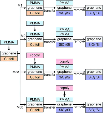 | ||
| Fig. 1 Schematic diagram of graphene wet transfer. M1, M2 and M3 denote method 1 [monolayer (1L) PMMA], method 2 [bilayer (2L) PMMA], and method 3 (PMMA + copolymer) described in the text. | ||
M1. 1L PMMA (conventional method): transfer as-is.
M2. 2L PMMA: spin-coat a second layer of PMMA identical to the first, then transfer.
M3. PMMA + copolymer: spin-coat a copolymer film at one of the following times.
(a) Before transfer to the silicon wafer (immediately after soft-baking the PMMA).
(b) After transferring the PMMA/graphene film onto the silicon wafer.
The copolymer we used is commercially available (MicroChem, MMA(8.5)MAA EL9), and contains PMMA and poly(methacrylic acid) (MAA) at a concentration of 9% in ethyl lactate (EL). We soft-baked the copolymer at 150 °C for 3 min after deposition.
Before the transfer step for all methods (see Fig. 1), we etched away any graphene from the back side of the Cu foil using oxygen plasma as described by Chen et al.12 We then dissolved the Cu foil by placing it in a 0.1 M solution of ammonium persulfate (Acros Organics, 98+%, UN1444), followed by a two-stage DI water bath (30 min each) to rinse the remaining polymer-supported graphene film and remove any residual Cu etchant. After rinsing, we scooped the floating polymer + graphene film onto a clean Si wafer and baked on a hot plate at 60 °C for 5 min. This was followed by an additional bake at 135 °C for 10 min to improve interfacial contact.9 In the final step, we removed any residual polymer by immersion in warm (55 °C) acetone for at least ten hours.
3 Results and discussion
3.1 Transfer method comparison
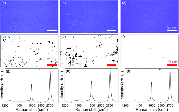
We characterized the transferred graphene films using optical microscopy, Raman spectroscopy (Renishaw inVia Reflex, 488 nm excitation), scanning electron microscopy (SEM, Carl Zeiss AURIGA), and terahertz time-domain spectroscopy (THz-TDS, Advantest TAS7500TS). To quantify the graphene continuity, we processed the optical micrographs as follows. First, we manually filled all visible holes with a color very dissimilar to the rest of the image. This step was not automated because image processing software can not reliably discern holes from other features such as residual PMMA or bilayer graphene regions. We then used the ImageJ software package13 to calculate the coverage of graphene regions and holes in each image from the percentage of pixels above or below a color threshold. Processing Fig. 2(a), (b) and (c) in this way yields the images shown in Fig. 2(d), (e) and (f) respectively. Black areas represent holes in the graphene, whereas white areas represent continuous graphene. We performed this analysis for nine separate areas within each transferred graphene sample (see ESI, S1†), and for all three methods shown in Fig. 1. We describe the results specific to each transfer method below.Based on our analysis of these three methods, we find that copolymer-assisted transfer (Method 3a) yields 99.8% continuous graphene, compared to 98.4% for 2L PMMA and 98.3% for 1L PMMA methods. In addition to having the highest average continuity, Method 3a also yields the most consistent results. The coverage standard deviation for the copolymer assisted method is 0.06% (see ESI, S1†), suggesting that the transferred graphene is highly continuous throughout the entire 1 cm × 1 cm transferred area.
We attribute the small holes in Fig. 2(c) to pinhole defects, which occur during CVD growth of graphene on rough Cu surfaces.17 Using a surface profilometer, we measured the RMS surface roughness (Rq) of our Cu foil at different positions after the CVD process. The roughness was approximately 150 nm, which is reasonable for commercially available unpolished Cu foil.18,19 We note that the Rq value is on the order of the thickness of the spin-coated film. Hence, it is likely that PMMA coverage and/or adhesion between the graphene and PMMA is inconsistent, which could lead to the few wrinkles or holes we did observe. This would also explain why graphene film transferred using Method 3b (copolymer added after transfer) was less continuous than graphene transferred using Method 3a (ESI, S2†). Based on these results, we determine that it is critical to add the copolymer layer prior to transfer.
When applied by spin-coating under identical conditions, the copolymer used here will form a film that is approximately twice the thickness of a PMMA film.20 As a result, the amount of residual solvent contained in the soft-baked copolymer layer will be considerably more than in an identically prepared PMMA layer. Moreover, relative evaporation rates are 0.22 for ethyl lactate and 0.32 for anisole, which means the copolymer solvent evaporates a bit slower than the PMMA solvent. This combination of greater solvent volume and slower evaporation rate means the underlying PMMA layer can be softened/relaxed to a greater extent by a copolymer layer than it could be by a second PMMA layer. Hence, the presence of copolymer before transfer (Method 3a) leads to improved contact between the graphene and PMMA,8 resulting in continuous transferred graphene as shown in Fig. 2(c). Conversely, if the copolymer is not added to the PMMA until after transfer (Method 3b), the solvent in the copolymer cannot effectively relax the PMMA because is has had more time to cure. Pits and pinholes can form in the PMMA as it cures,21 resulting in considerably more cracks, holes, and wrinkles in the transferred graphene.
3.2 Scanning electron microscopy analysis
We used SEM imaging to characterize the morphologies of three graphene films transferred using 1L PMMA, 2L PMMA, and PMMA + copolymer. Voids and a considerable amount of wrinkles are visible in Fig. 3(a) and (b), whereas the amount of transfer-induced damage visible in Fig. 3(c) is negligible.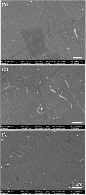 | ||
| Fig. 3 Scanning electron micrographs of graphene film transferred using (a) 1L PMMA, (b) 2L PMMA, and (c) PMMA + copolymer (Method 3a). Scale bars are 2 μm for all images. | ||
3.3 Spectroscopic analysis of copolymer-assisted transfer
We performed large area Raman mapping to further evaluate the continuity and quality of the graphene transferred using copolymer. Fig. 4 shows a Raman map of continuous graphene transferred using Method 3a (copolymer added before transfer). No cracks, holes, or wrinkles are visible in the image area. Superimposed Raman maps from six locations show essentially no regions with I2D/IG < 1, indicating mostly monolayer and some bilayer graphene,16,22 which is consistent with the optical micrographs shown in Fig. 2. Similarity in the Raman maps suggests that these six areas are representative of the entire 1 cm × 1 cm transferred graphene.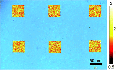 | ||
| Fig. 4 Raman map of 2D/G intensity ratio of graphene transferred using Method 3a (PMMA + copolymer in Fig. 1). | ||
As an additional metric, we used THz-TDS in the range of 0.5 THz to 2.5 THz to extract the complex conductivity of each of the graphene samples.23,24 We do this by illuminating five random areas on each graphene sample with THz light (1 mm spot size), and converting the time-domain signal into frequency-domain via Fourier transform. We then compare the measured THz signal with that of a bare SiO2/Si reference substrate to determine the Fresnel reflection coefficient at the substrate–graphene interface.25 Finally, we extract the complex conductivity and simultaneously fit the real and imaginary parts to the Drude–Smith model.26 One of the two fitting parameters is the scattering time,27 which we plot in Fig. 5. Also plotted in the same figure are the statistical distributions of area coverage calculated for graphene transferred using each of the three methods shown in Fig. 1. We see that the scattering time tends to be longer when the graphene coverage is higher. Although a quantitative relation between coverage and scattering time is not well established, qualitatively we expect the scattering time to increase when holes, cracks, and other scattering sites are reduced. This correlation between higher graphene coverage and longer charge-carrier scattering time further supports our conclusion based on Raman and image analysis that the copolymer-assisted graphene transfer method proposed here (Method 3a) yields nearly complete graphene continuity.
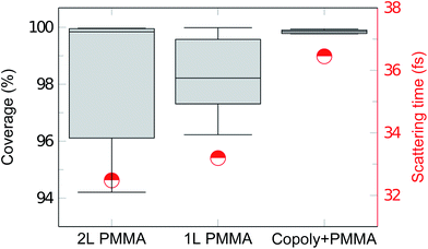 | ||
| Fig. 5 Boxplot of the area coverage (left axis) and values of scattering time (right axis) for graphene transferred using different methods. | ||
4 Conclusions
In summary, we report the first copolymer-assisted graphene transfer protocol, and demonstrate square-centimeter-scale transfer of monolayer graphene with nearly complete continuity. We find this approach to be more effective at reducing small holes and eliminating cracks and wrinkles than methods that use only PMMA. We attribute this difference to a larger volume of solvent contained in the thicker copolymer layer which, when combined with the slightly slower evaporation rate of the copolymer solvent, is more effective at relaxing the underlying PMMA. This method is only effective if the copolymer is added soon after soft-baking the PMMA, i.e., before the PMMA has time to cure. We expect that the addition of copolymer to an already familiar wet transfer method will help mitigate defect formation during graphene transfer. This will facilitate the use of high quality, continuous graphene in applications requiring large footprints, such as those involving arrays of graphene-based elements.Conflicts of interest
There are no conflicts to declare.Acknowledgements
This work was partially supported by the US Air Force Office of Scientific Research under grant # FA9550-16-1-0188.References
- G. Jo, M. Choe, S. Lee, W. Park, Y. H. Kahng and T. Lee, Nanotechnology, 2012, 23, 112001 CrossRef PubMed.
- S. Bae, H. Kim, Y. Lee, X. Xu, J.-S. Park, Y. Zheng, J. Balakrishnan, T. Lei, H. R. Kim, Y. I. Song, Y.-J. Kim, K. S. Kim, B. Özyilmaz, J.-H. Ahn, B. H. Hong and S. Iijima, Nat. Nanotechnol., 2010, 5, 574–578 CrossRef CAS PubMed.
- J. Kang, S. Hwang, J. H. Kim, M. H. Kim, J. Ryu, S. J. Seo, B. H. Hong, M. K. Kim and J. B. Choi, ACS Nano, 2012, 6, 5360–5365 CrossRef CAS PubMed.
- G. B. Barin, Y. Song, I. F. Gimenez, A. G. Souza Filho, L. S. Barreto and J. Kong, Carbon, 2015, 84, 82–90 CrossRef.
- Y. Ahn, H. Kim, Y. H. Kim, Y. Yi and S. I. Kim, Appl. Phys. Lett., 2013, 102, 091602 CrossRef.
- J. W. Suk, W. H. Lee, J. Lee, H. Chou, R. D. Piner, Y. Hao, D. Akinwande and R. S. Ruoff, Nano Lett., 2013, 13, 1462–1467 CrossRef CAS PubMed.
- S. Kim, S. Shin, T. Kim, H. Du, M. Song, C. Lee, K. Kim, S. Cho, D. H. Seo and S. Seo, Carbon, 2016, 98, 352–357 CrossRef CAS.
- X. S. Li, Y. W. Zhu, W. W. Cai, M. Borysiak, B. Y. Han, D. Chen, R. D. Piner, L. Colombo and R. S. Ruoff, Nano Lett., 2009, 9, 4359–4363 CrossRef CAS PubMed.
- X. Liang, B. A. Sperling, I. Calizo, G. Cheng, C. A. Hacker, Q. Zhang, Y. Obeng, K. Yan, H. Peng, Q. Li, X. Zhu, H. Yuan, A. R. Hight Walker, Z. Liu, L.-M. Peng and C. A. Richter, ACS Nano, 2011, 9144–9153 CrossRef PubMed.
- S. Cai, X. Liu, J. Huang and Z. Liu, RSC Adv., 2017, 7, 48333–48340 RSC.
- Y. Hao, M. S. Bharathi, L. Wang, Y. Liu, H. Chen, S. Nie, X. Wang, H. Chou, C. Tan, B. Fallahazad, H. Ramanarayan, C. W. Magnuson, E. Tutuc, B. I. Yakobson, K. F. McCarty, Y.-W. Zhang, P. Kim, J. Hone, L. Colombo and R. S. Ruoff, Science, 2013, 342, 720–723 CrossRef CAS PubMed.
- M. Chen, G. Li, W. Li and D. Stekovic, Carbon, 2016, 110, 286–291 CrossRef CAS.
- M. Abramoff, P. Magalhaes and S. Ram, Biophotonics Int., 2004, 11, 36–42 Search PubMed.
- Y.-P. Hsieh, Carbon, 2013, 67, 417–423 CrossRef.
- Y.-C. Lin, C.-C. Lu, C.-H. Yeh, C. Jin, K. Suenaga and P.-W. Chiu, Nano Lett., 2012, 12, 414–419 CrossRef CAS PubMed.
- A. C. Ferrari, J. C. Meyer, V. Scardaci, C. Casiraghi, M. Lazzeri, F. Mauri, S. Piscanec, D. Jiang, K. S. Novoselov, S. Roth and A. K. Geim, Phys. Rev. Lett., 2006, 187401 CrossRef CAS PubMed.
- S. S. Roy, R. M. Jacobberger, C. Wan and M. S. Arnold, Carbon, 2016, 100, 1–6 CrossRef.
- B. Zhang, W. H. Lee, R. Piner, I. Kholmanov, Y. Wu, H. Li, H. Ji and R. S. Ruoff, ACS Nano, 2012, 6, 2471–2476 CrossRef CAS PubMed.
- S. M. Kim, A. Hsu, Y.-H. Lee, M. Dresselhaus, T. Palacios, K. K. Kim and J. Kong, Nanotechnology, 2013, 24, 365602 CrossRef PubMed.
- MicroChem Corp., NANO PMMA and copolymer, 2012, pp. 2–9 Search PubMed.
- N. G. Semaltianos, Microelectron. J., 2007, 38, 754–761 CrossRef CAS.
- L. M. Malard, M. A. Pimenta, G. Dresselhaus and M. S. Dresselhaus, Phys. Rep., 2009, 473, 51–87 CrossRef CAS.
- Y. Zhou, Y. E. L. Zhu, M. Qi, X. Xu, J. Bai, Z. Ren and L. Wang, Carbon, 2016, 96, 1129–1137 CrossRef CAS.
- J. D. Buron, D. H. Petersen, P. Bøggild, D. G. Cooke, M. Hilke, J. Sun, E. Whiteway, P. F. Nielsen, O. Hansen, A. Yurgens and P. U. Jepsen, Nano Lett., 2012, 12, 5074–5081 CrossRef CAS PubMed.
- F. Vandrevala, A. Karmakar, J. M. Jornet and E. Einarsson, 41st International Conference on Infrared, Millimeter, and Terahertz waves (IRMMW-THz), 2016, pp. 1–2 Search PubMed.
- N. V. Smith, Phys. Rev. B, 2001, 64, 155106 CrossRef.
- P. R. Whelan, K. Iwaszczuk, R. Wang, S. Hofmann, P. Bøggild and P. U. Jepsen, Opt. Express, 2017, 25, 2725–2732 CrossRef.
Footnotes |
| † Electronic supplementary information (ESI) available: Optical micrographs and details on image analysis. See DOI: 10.1039/c7ra12328k |
| ‡ Present address: Singapore University of Technology and Design, Singapore. |
| This journal is © The Royal Society of Chemistry 2018 |

