DOI:
10.1039/C7RA12049D
(Paper)
RSC Adv., 2018,
8, 987-993
Graphene oxide as an additive to improve perovskite film crystallization and morphology for high-efficiency solar cells
Received
2nd November 2017
, Accepted 20th December 2017
First published on 3rd January 2018
Abstract
The quality of a perovskite film has a great impact on its light absorption and carrier transport, which is vital to improve high-efficiency perovskite solar cells (PSCs). Herein, it is demonstrated that graphene oxide (GO) can be used as an effective additive in the precursor solution for the preparation of high-quality solution-processed CH3NH3PbI3 (MAIPbI3) films. It is evidenced by scanning electron microscopy that the size of the grains inside these films not only increases but also becomes more uniform after the introduction of an optimized amount of 1 vol% GO. Moreover, 1 vol% GO also enhances the crystallization of perovskite film with intact preferential out-of-plane orientation as proven by 2-dimensional grazing-incidence X-ray diffraction. As a consequence of the improved film quality, enhanced charge extraction efficiency and optical absorption are demonstrated by photoluminescence (PL) spectroscopy and UV-visible absorption spectroscopy, respectively. Using 1 vol% GO, the fabricated champion heterojunction PSC with a structure of ITO/SnO2/perovskite/spiro-OMeTAD/Au shows a significant power conversion efficiency increase to 17.59% with reduced hysteresis from 16.10% for the champion device based on pristine perovskite. The present study thus proposes a simple approach to make use of GO as an effective and cheap addictive for high-performance PSCs with large-scale production capability.
Introduction
In the past few years, organic–metal halide perovskite solar cells (PSCs) have drawn massive attention as a new member of photovoltaic (PV) devices due to their excellent characteristics including broad light absorption range, ambipolar charge transport, and long carrier diffusion length.1–4 The power conversion efficiency (PCE) has skyrocketed from 3.8% to 22.1% since 2009.5,6 In addition, the performance can be further enhanced by meticulously optimizing perovskite composition, device structure, and the processing methods.7–14
Perovskite thin films can be prepared by one or two-step solution process, sequential deposition, and co-evaporation.7–9,15 A one-step solution process is a more preferable method than others owing to its simplicity and low annealing temperature. The perovskite crystallization process plays an important role in the formation of high quality one-step solution processed perovskite thin films for high performance PSCs. Poor crystallinity of a perovskite thin film is detrimental to its resultant PSC device performance due to a large amount of defects within the film leading to lots of serious recombination and voltage loss.16–19 Superior crystallinity of a perovskite thin film not only means a highly quality film with few defects, but also favors the interfacial contact between the perovskite thin film and the transport layer to enhance charge separation.20,21 Many factors are known to affect perovskite crystallization including the solvents used, solution concentration, precursor composition, post annealing temperature, and processing environment, which can be adjusted to improve crystallization for high quality perovskite thin films.22–25 Additives intentionally added into the precursor solution for the preparation of perovskite thin films are known to be able to effectively enhance the perovskite film crystallization and morphology for high performance PSCs.26,27 For instance, A. K. Y. Jen et al. introduced 1,8-diiodooctance (DIO) as an additive into the precursor solution during the film fabrication process, and DIO could temporarily coordinate with Pb2+ during crystal nucleation and growth, which tends to promote homogenous nucleation and likely modifies interfacial energy favorably.17 Similarly, Ding et al. adopted NH4Cl as an additive to fabricate perovskite thin films. The films turned out to be highly crystallized with excellent morphology, leading to remarkably enhanced device performance.28 Chen et al. found that 1-chloronaphthalene (CN) additive was beneficial to regulate the crystallization transformation kinetics of perovskite for high-quality perovskite thin films.29 Huang et al. introduced organic halide salts as a processing additive to modulate the morphology and crystallinity of the perovskite light-absorbing layer in perovskite/fullerene planar-heterojunction solar cells, which also serves as an interfacial modifier to improve the electrical contact of the [6,6]-phenyl-C61-butyric acid methyl ester (PCBM)/Al electron-collecting electrode.30 Su et al. used poly(ethyleneglycol) (PEG) additive to tune the morphology of the perovskite layer by retarding the growth and aggregation of perovskite crystals with the formation of a continuous and uniform film.31 Wu et al. improved the quality of the perovskite thin films by adding PCBM into PbI2 precursor solution for a low-temperature two-step solution process, and found that PCBM played a critical role in filling pinholes and vacancies, resulting in a film with large grains and fewer grain boundaries.32
On the other hand, graphene oxide (GO) has attracted a great deal of attentions due to its excellent electronic properties as well as its multi-functionalities, reliability, low production costs, large-scale production capability, and good dispersibility in many solvents. GO is a layered material with various oxygen-containing functional groups (carboxyl, carbonyl, phenol, lactone, and quinone) on its basal plane and edge. The distribution of hydrophilic and hydrophobic properties induced by its functional groups from the edge to the center make it an ideal surfactant.33–36 In addition, its heterogeneous chemical and electronic structures make GO a potential material for retarding electron recombination in high-performance PSCs. According to previous works, GO has already been demonstrated as an excellent interfacial material.37–39 For example, Wang et al. improved the photovoltaic performance of PSCs using GO as an amphiphilic modifier to enhance the interface contact between perovskite and the hole transport layer.34 The introduction of ammonia modified GO layer into PSC devices by Yang et al. improved their device performance and perovskite structure stability.40 Sun et al. employed GO as hole conductor on perovskite thin films in inverted planar heterojunction PSCs, which improved the perovskite crystallization with enhanced hole extraction.41 There are also reports about GO as a better hole transport layer than PEDOT:PSS to achieve enhanced PSC performance.42,43 In addition, Ding and Yuan et al. reported enhanced efficiency of mesoscopic perovskite solar cells by adding graphene quantum dots (GQDs) as additive into precursor to passivate the grain boundaries of CH3NH3PbI3.44 Nevertheless, the preparation of GQDs usually requires special equipment and suffers low production yield as well as critical synthesis conditions.45–48 Therefore, GQDs are unlikely a promising additive candidate for low-cost large area production of PSCs. To the contrary, GO itself can be easily and cheaply synthesized in large quantity, which could be a better additive candidate in the preparation of high quality perovskite thin films in PSCs.35,36,49–51 Indeed, Hagfeldt et al. introduced nitrogen-doped reduced graphene oxide (N-RGO) into the perovskite layer of PSCs, which tuned both morphological features and recombination dynamics, resulting in better PSC performance.52 Moreover, they found that native RGO barely increase the grain size and optical absorption but still enhance the device performance due to surface-passivation of the perovskite by graphene sheets resulting in improved hole selectivity and reduced recombination at the perovskite/spiro-OMeTAD interface. In this work, it is further proven that the crystallization of perovskite thin films prepared by one-step method can be improved simply by adding GO into their perovskite precursor solution. Using an optimization amount of 1 vol%, GO is demonstrated to promote the perovskite film quality with improved crystallization as well as large and uniform grains. Besides, it is also found that the incorporation of GO efficiently promote the charge extraction at perovskite/spiro-OMeTAD interfaces which may be due to the superior electronic properties of GO and the improved interfacial contact. Finally, the fabricated champion heterojunction PSC with a structure of ITO/SnO2/perovskite/spiro-OMeTAD/Au using 1 vol% GO shows significant power conversion efficiency increase from 16.10% for that based on pristine perovskite to 17.59%. The present study demonstrates GO as an effective and cheap addictive for high-performance PSCs with large-scale production capability.
Results and discussion
Photovoltaic performance
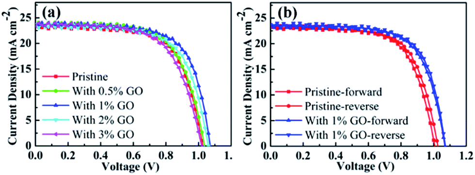
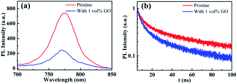
To find out the effects of GO on PSC performance, current–voltage (J–V) curves measured on the fabricated champion devices based on MAPbI3 using different amount of GO with a concentration up to 3 vol% are reported in Fig. 1. Their photovoltaic parameters derived from Fig. 1(a) are listed in Table 1. The pristine MAPbI3 champion device exhibits an open circuit voltage (VOC) of 1.026 V, a short circuit current density (JSC) of 23.41 mA cm−2, a fill factor (FF) of 67.08%, and a PCE of 16.10%, whereas the MAPbI3 champion device with 1 vol% of GO achieves a VOC of 1.072 V, a JSC of 23.73 mA cm−2, a FF of 69.14%, and a PCE of 17.59%, which obviously is the best among all the fabricated champion devices with an amount of GO from 0 to 3 vol%. It can be seen from Table 1 that VOC, FF, and PCE increase with the GO concentration internally and then drops quite fast after reaching their maxima at an amount of 1 vol%, and that JSC increases similarly with the GO concentration but reaches its maximum at 2 vol%. In addition, Fig. 1(b) reports the reverse and forward scanned current–voltage curves for the pristine MAPbI3 PSC and that with 1 vol% of GO, which clearly indicates that the introduction of 1 vol% GO also reduces the hysteresis effectively. For a better comparison, their device parameters for both forward and reverse scans are summarized in Table 2. Therefore, all these results indicate that 1 vol% of GO is the most effective addictive concentration to enhance the PSCs performance with reduced hysteresis.
 |
| | Fig. 1 (a) J–V curves of the fabricated champion PSCs with different amount of GO in the perovskite precursor solution; (b) the forward and reverse scans for the champion pristine PSC without GO and that with 1 vol% of GO. | |
Table 1 Photovoltaic parameters of the ITO/SnO2/MAPbI3/spiro-OMeTAD/Au PSCs with different amount of GO
| GO (vol%) |
J
SC (mA cm−2) |
V
OC (V) |
FF (%) |
PCE (%) |
PCEAVE (%) |
| 0 |
23.41 |
1.026 |
67.08 |
16.10 |
14.68 ± 1.01 |
| 0.5 |
23.50 |
1.036 |
67.68 |
16.48 |
15.14 ± 0.72 |
| 1 |
23.73 |
1.072 |
69.14 |
17.59 |
16.35 ± 0.72 |
| 2 |
23.81 |
1.062 |
65.88 |
16.66 |
14.42 ± 1.06 |
| 3 |
23.44 |
1.019 |
65.31 |
15.59 |
13.36 ± 1.46 |
Table 2 The device parameters for the champion pristine PSC without GO and that with 1 vol% of GO derived from both forward and reverse scans in Fig. 1(b)
| GO (vol%) |
J
SC (mA cm−2) |
V
OC (V) |
FF (%) |
PCE (%) |
| 0-Forward |
23.21 |
1.007 |
66.69 |
15.59 |
| 0-Reverse |
23.41 |
1.026 |
67.08 |
16.10 |
| 1-Forward |
23.45 |
1.069 |
68.50 |
17.17 |
| 1-Reverse |
23.73 |
1.072 |
69.14 |
17.59 |
SEM results
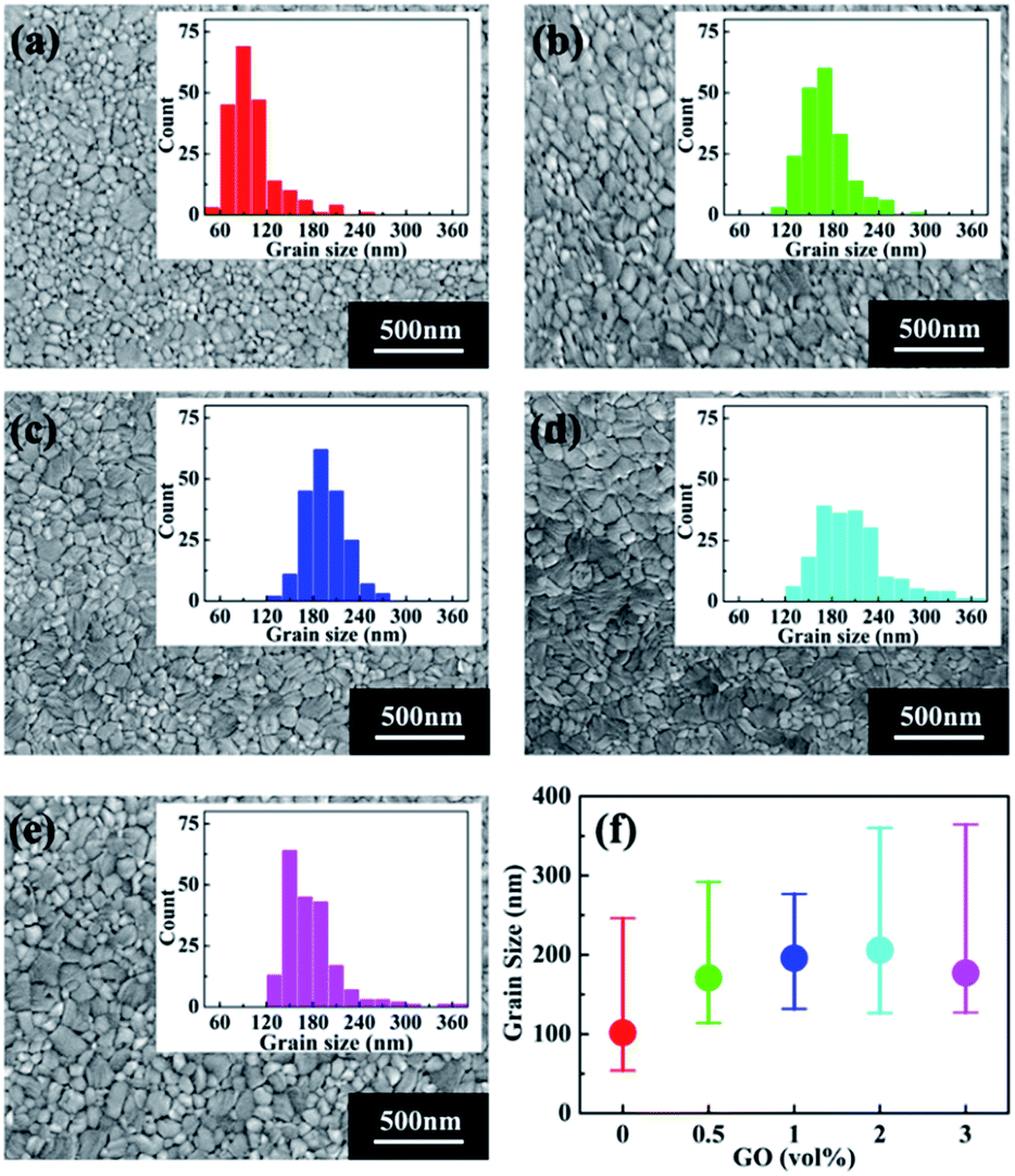
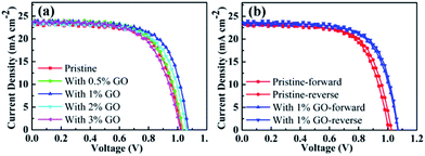
To study the possible reason for the PSC performance enhancement brought by GO, scanning electron microscopy (SEM) was conducted to investigate the morphology of perovskite thin films with different amount of GO, which are shown in Fig. 2(a)–(e). The insert in each SEM image is the grain size distribution of the corresponding film. For a better comparison, the average grain size as the function of GO amount is reported in Fig. 2(f). From these results, the average grain size of the pristine perovskite thin film is 100 nm, which quickly becomes larger with the increasing GO amount till 1 vol% to about 200 nm. After that, the average size still increases slightly at 2 vol% and drops at 3 vol%. It is also noticed that the film with 1 vol% GO has the narrowest grain size distribution indicating this film has the most uniform morphology among all the films.53
 |
| | Fig. 2 SEM images of perovskite thin films (a) pristine, with (b) 0.5 vol%, (c) 1 vol%, (d) 2 vol%, and (e) 3 vol% GO in the perovskite precursor. The insert in each image shows the corresponding grain size distribution. (f) The average grain size as the function of GO amount. | |
GIXRD results
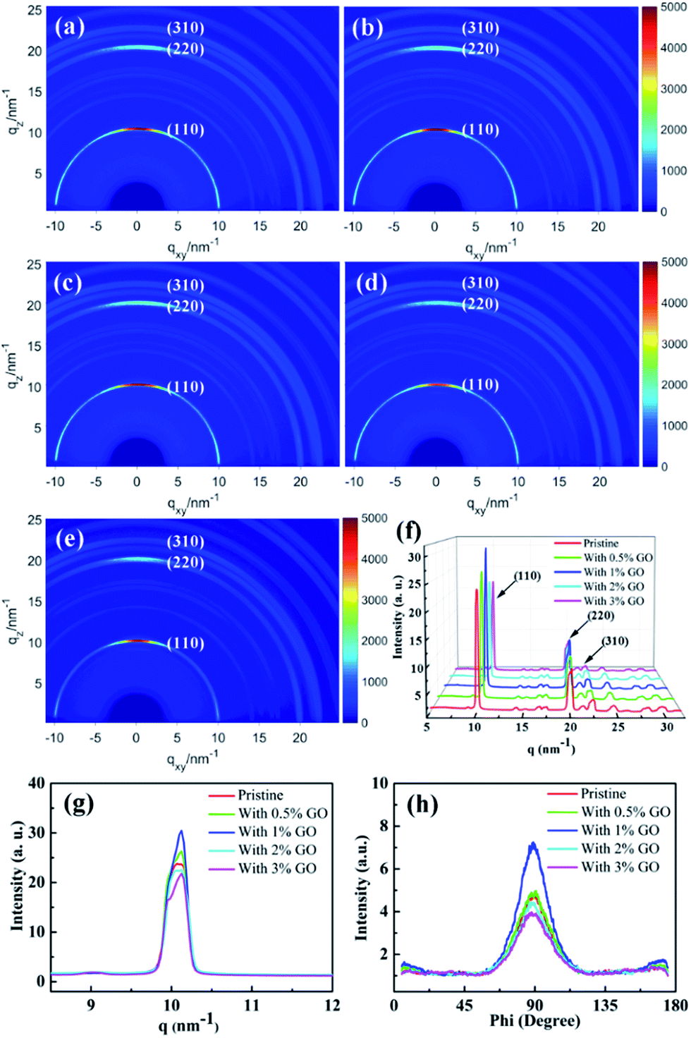
To investigate the crystallization of the fabricated perovskite film directly, two-dimensional GIXRD measurements were performed on the perovskite thin films with different amount of GO on the ITO/SnO2 substrates. Fig. 3(a)–(e) report the obtained GIXRD patterns, which show scattering rings at q ≈ 10, 20, and 23 nm−1, consistent with the typical (110), (220), and (310) tetragonal MAPbI3 diffraction, respectively.54Fig. 3(f) reports the azimuthally integrated intensity profiles derived from the diffraction patterns for the different films, which indicates quantitatively their crystallization degree. The dominant (110), (220), and (310) peaks in Fig. 3(f) demonstrate that these films possess good crystallization degree with large grains, which are proven more clearly by the strong and sharp (110) peak in Fig. 3(g). It is clear that the film with 1 vol% GO displays the highest and sharpest perovskite (110) diffraction peak due to its highest crystallization degree, which is obviously vital to the enhanced performances of the present optimized PSCs.41,54,55 To study the crystallization preferential orientation, the radially integrated intensity profiles derived from the diffraction patterns at q ≈ 10 nm−1 for the perovskite (110) plane in the films with different amount of GO are present in Fig. 3(h). The dominant peaks at an azimuth angle of 90° demonstrate that all the films exhibit a preferential out of plane orientation, which favor the interfacial charge transporting.56–58 Thus, the presence of GO did not change the out-of-plane preferential order of the perovskite crystallization. It becomes clear that 1 vol% is the optimized amount of GO to achieve the best quality perovskite film among all these films with best crystallization and morphology as evidenced by the SEM and GIXRD results. The excellent electronic properties of GO and/or the functional groups on the GO surface make GO likely serve as efficient chemical reaction and crystallization nucleation centers during the perovskite film growth, promoting chemical reaction and enhancing crystallinity with large grains and few defects. When the amount of GO is less than 1 vol% and they should be able to distribute uniformly in the precursor solution, the increasing amount of GO means more reaction and nucleation centers during the formation of perovskite to facilitate the film crystallization leading to larger grains and more uniform morphology. In fact, it was noticed that the prepared precursor solution with less than 3 vol% GO stayed clear and transparent for several days, which proves that GO can distribute uniformly in the precursor solution. With more than 1 vol% GO present in the precursor solution, however, GO could segregate occasionally during the formation of perovskite leading to randomly distributed and even fewer reaction and nucleation centers causing worse crystallization and morphology. While the optimal amount of 1 vol% GO is proven to achieve most enhanced crystallization and best morphology in the perovskite films, it will be shown later to facilitate carrier extraction and reduce exciton recombination as well as improve the optical absorption. All these achievements induced by 1 vol% GO should be the main reason leading to the best PSC device.
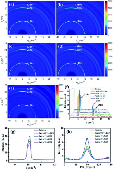 |
| | Fig. 3 Two-dimensional GIXRD patterns of (a) the pristine perovskite thin film, (b) that with 0.5 vol%, (c) 1 vol%, (d) 2 vol%, and (e) 3 vol% GO in perovskite precursor, respectively; the azimuthally integrated intensity profiles derived from the diffraction patterns for the different films in (f) and these profiles around (110) peak in (g), respectively; (h) the radially integrated intensity profiles derived from the diffraction patterns at q ≈ 10 nm−1 with different amount of GO. | |
UV-vis and EQE spectra
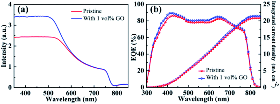
Fig. 4(a) reports the UV-vis absorption spectrum of a pristine CH3NH3PbI3 film directly spin-coated on clean glass and that of another film with 1 vol% GO. The obvious absorption decrease after 500 nm as well as the absorption onset at about 790 nm in these two spectra are characteristics of MAPbI3 spectrum.59 In comparison with the pristine film, the optical absorption for the film containing GO is almost identical to that for the pristine film from 600 to 800 nm but higher in the near UV region from 350 to 550 nm, which should be mainly due to the improved crystallinity of perovskite thin film by GO as evidenced by the GIXRD and SEM leading to higher JSC in the PSC containing GO. Fig. 4(b) reports the EQE spectra with integrated current density of PSCs based on a pristine perovskite film and another with 1 vol% GO fabricated following the same processes described before. The broad spectral response in the range of 350–800 nm agrees with the absorption spectra of perovskite thin films in Fig. 4(a). The integrated JSC values are calculated to be 20.84 mA cm−2 for the PSC based on the pristine film and 21.49 mA cm−2 for that with 1 vol% GO, respectively, which proves again that GO is an efficient addictive to improve the PSC performance as demonstrated in J–V measurements.
 |
| | Fig. 4 (a) UV-vis absorption spectra of a pristine perovskite film and another with 1 vol% GO; (b) EQE spectra with integrated current density of the PSC based on the pristine perovskite film and that with 1 vol% GO. | |
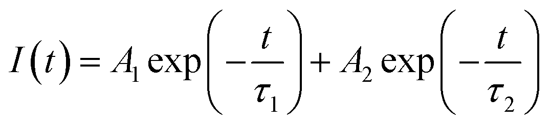
PL and TRPL
Photoluminescence characterization was widely used in photovoltaic related fields to obtain information about charge carrier dynamics in the active layer or at the interface between the active layer and transport layers. In order to investigate the hole extraction efficiency from perovskite to the transport layer, perovskite films deposited on glass substrate and then coated with a spiro-OMeTAD hole transport layer were used for the steady-state photoluminescence (PL) and time-resolved photoluminescence (TRPL) measurements. Before the PL experiments, UPS spectra of these films were measured, which shows that the work function, the valance band maximum, and other valence band photoemission features of the perovskite films are not changed by the introduction of GO, indicating a few vol% GO addictive barely changes the electronic structures of the perovskite films. From the normalized steady-state PL spectra in Fig. 5(a), it is clear that the PL intensity of the perovskite film with 1 vol% GO is much lower (i.e., high PL quenching) than that of the pristine film, which is associated with the efficient charge separation and extraction (or injection) from the photoactive perovskite to the charge-transport layer. Therefore, Fig. 5(a) indicated that GO can obviously improve the charge extraction, which may be related to the superior electronic properties of GO or improved interface contact between high quality perovskite and hole transport layer. As can be seen from the TRPL spectra in Fig. 5(b), the film with GO decay much faster than the pristine film. To quantitatively analysing the carrier lifetime, the TRPL profiles can be fitted by the following bi-exponential function:
 |
| | Fig. 5 (a) Steady-state photoluminescence (PL) and (b) time-resolved photoluminescence (TRPL) spectra of glass/MAPbI3/spiro-OMeTAD without or with 1 vol% GO. | |
In the function, τ1 and τ2 represent decay characteristic time for two decay components: the fast decay τ1 reflects diffusion of initially photo-generated excitons into defects or charge selection layers, and the slow decay τ2 is associated with the exciton lifetime of perovskite thin film. General, a small τ2 value will indicate a fast exciton- or hole-diffusion process.60–63 The fitted parameters derived from the two spectra are summarized in Table 3. As shown in Table 3, both τ1 and τ2 for the film with GO are smaller than the corresponding values for the pristine film, proving that GO obviously promote hole extraction and transport. The enhanced carrier extraction must be associated with the GO in the perovskite thin film. First of all, the better film morphology could improve the contact between perovskite and transport layer spiro-OMeTAD, which promotes the hole injection into spiro-OMeTAD, leading to reduce recombination at the interface.56 Secondly, the large and uniform grains will reduce grain boundary and defects, which allow the exciton transport more easily. Thirdly, GO possibly reside at the grain boundaries or surface could be effectively bonded with MAPbI3 and passivate the dangling bonds to eliminate electron raps, which will facilitate the charge extraction. In addition, the electrons will transfer faster through GO in the perovskite film to separate more quickly from the holes, which could explain the increases of JSC, VOC and FF. As exciton could transport in the film more freely leading to a longer diffusion length as well as faster a diffusion rate, hysteresis is also eliminated effectively as demonstrated before.
Table 3 Fitted parameters derived from TRPL spectra
| GO (vol%) |
τ
1 (ns) |
τ
2 (ns) |
| 0 |
4.07 |
34.95 |
| 1 |
3.86 |
26.92 |
Experimental
PSCs fabrication
To prepare perovskite precursor solution, 269 mg methylammonium iodide (MAI, 99.9%, MaterWin New Materials Co. Ltd, Shanghai) and 780 mg lead(II) iodide (PbI2, 99%, Aldrich) powder were dissolved in 880 μL N,N-dimethylformamide (DMF, anhydrous, 99.8%, Sigma-Aldrich) solution and then added by 120 μL dimethyl sulfoxide (DMSO, anhydrous, 99.9%, Sigma-Aldrich). The precursor solution was stirred for 1 h at 60 °C before adding GO. GO was fabricated by a modified Hummers method as reported.64 The as-prepared GO was ground into fine powder, which was dispersed in DMF at 0.5 mg mL−1 and ultrasonicated for 4 hours. Finally, different amount of GO solution was added into precursor solution to prepare a mixed solution with different GO concentration (0.5, 1, 2, and 3 vol%), which was stirred at 60 °C for another 2 h before usage.
Indium tin oxide (ITO) substrates (12 Ω sq−1, 1.5 cm × 1.5 cm) were cleaned sequentially in an ultrasonic solvent bath of detergent, deionized water, acetone, and alcohol. After dried in a stream of nitrogen, the substrates were treated in Ultraviolet Ozone (UVO) cleaner for 10 min. Then, the 2.67% SnO2 solution was coated on ITO, and annealed at 150 °C for 30 min in air. The substrates were then transferred into a glove box (H2O and O2 < 1.0 ppm) filled with N2. Perovskite layer was formed by spin-coating precursor solution at 3000 rpm for 30 s, 1 mL of ether was dripped just after the spin coating started. Then the films were annealed at 100 °C for 5 min. After cooling to room temperature, 2,2′,7,7′-tetrakis(N,N-bis(p-methoxyphenyl)amino)-9,9′-spirobifluorene (spiro-OMeTAD) solution doped with bis(trifluoromethylsulfonyl)-imide lithium salt (Li-TFSI) and tert-butylpyridine (TBP) was spin-coated at 2000 rpm for 45 s. In the end, the films were transferred into a vacuum chamber, where gold electrodes with a thickness of 100 nm were evaporated under high vacuum (<5 × 10⁻⁶ Torr) through a shadow mask. Therefore, the fabricated planar PSC devices have an architecture of ITO/SnO2/perovskite/spiro-OMeTAD/Au.
Characterization
Synchrotron based GIXRD (grazing-incidence X-ray diffraction) was performed at the BL14B1 beamline endstation of Shanghai Synchrotron Radiation Facility (SSRF), using X-ray with a wavelength of 0.06887 nm with an incident angle of 0.20°.65 The diffractive patterns were recorded by an area detector (charge coupled device, CCD). A cold field-emission scanning electron microscope (SEM, Hitachi S-4800) was used to obtain top view morphology. UV-vis spectra was conducted by a UV-VIS-NIR 3600 spectrophotometer (Shimadzu). While a xenon light source solar simulator (450 W, Oriel, model 9119) with an AM 1.5G filter (Oriel, model 91192) was used to give an irradiance of 100 mW cm−2 at the surface of the solar cells, their photovoltaic characterization was carried out by using a Keithley 2400 digital source meter. The effective area of each cell was 0.102 cm2 defined by masks for all the photovoltaic devices. External quantum efficiencies (EQE) were measured by an Enli Technology (Taiwan) EQE measurement system. Ultraviolet photoemission spectroscopy (UPS) was performed in an ultrahigh vacuum (UHV) system by using a PHOIBOS 100 analyzer together with a helium light lamp (He I: 21.2 eV). Transient-state photoluminescence (PL) was measured by FLS980 (Edinburgh Instruments Ltd.) with an excitation at a wavelength of 470 nm.
Conclusions
In conclusion, by adding 1 vol% GO into the perovskite precursor solution to prepare the perovskite films, performance of resultant PSCs can be enhanced with a PCE increase from 16.10% to 17.59% with significantly reduced hysteresis effects. These performance achievements can be attributed to the crystallization and morphology improvement brought by GO as additive, which not only facilitates carrier extraction and reduce exciton recombination but also improves the optical absorption. Thus, GO is proven to be an effective additive for the preparation of high quality solution-processed perovskite towards high-efficiency PSC for large-scale production capability.
Conflicts of interest
There are no conflicts to declare.
Acknowledgements
This work is supported by the National Natural Science Foundation of China (Grant No. 11675252, 11175239, and U1632265), and One Hundred Talents Project of the Chinese Academy of Sciences. The authors thank beamline BL14B1 at Shanghai Synchrotron Radiation Facility (SSRF) for providing the beam time.
Notes and references
- L. Meng, J. You, T.-F. Guo and Y. Yang, Acc. Chem. Res., 2016, 49, 155–165 CrossRef CAS.
- S. D. Stranks, P. K. Nayak, W. Zhang, T. Stergiopoulos and H. J. Snaith, Angew. Chem., Int. Ed., 2015, 54, 3240–3248 CrossRef CAS.
- J. H. Heo, D. H. Song, B. R. Patil and S. H. Im, Isr. J. Chem., 2015, 55, 966–977 CrossRef CAS.
- G. Niu, X. Guo and L. Wang, J. Mater. Chem. A, 2015, 3, 8970–8980 RSC.
- A. Kojima, K. Teshima, Y. Shirai and T. Miyasaka, J. Am. Chem. Soc., 2009, 131, 6050–6051 CrossRef CAS.
- W. S. Yang, B.-W. Park, E. H. Jung, N. J. Jeon, Y. C. Kim, D. U. Lee, S. S. Shin, J. Seo, E. K. Kim, J. H. Noh and S. I. Seok, Science, 2017, 356, 1376–1379 CrossRef CAS.
- J. Burschka, N. Pellet, S.-J. Moon, R. Humphry-Baker, P. Gao, M. K. Nazeeruddin and M. Grätzel, Nature, 2013, 499, 316–319 CrossRef CAS.
- M. Liu, M. B. Johnston and H. J. Snaith, Nature, 2013, 501, 395–398 CrossRef CAS.
- N. J. Jeon, J. H. Noh, Y. C. Kim, W. S. Yang, S. Ryu and S. I. Seok, Nat. Mater., 2014, 13, 897–903 CrossRef CAS.
- N. Ahn, D.-Y. Son, I.-H. Jang, S. M. Kang, M. Choi and N.-G. Park, J. Am. Chem. Soc., 2015, 137, 8696–8699 CrossRef CAS.
- Y. Chen, T. Chen and L. Dai, Adv. Mater., 2015, 27, 1053–1059 CrossRef CAS.
- J.-H. Im, J. Luo, M. Franckevičius, N. Pellet, P. Gao, T. Moehl, S. M. Zakeeruddin, M. K. Nazeeruddin, M. Grätzel and N.-G. Park, Nano Lett., 2015, 15, 2120–2126 CrossRef CAS.
- K.-L. Wu, A. Kogo, N. Sakai, M. Ikegami and T. Miyasaka, Chem. Lett., 2015, 44, 321–323 CrossRef CAS.
- Q.-Y. Xu, D.-X. Yuan, H.-R. Mu, F. Igbari, Q. Bao and L.-S. Liao, Nanoscale Res. Lett., 2016, 11, 248 CrossRef.
- W. S. Yang, J. H. Noh, N. J. Jeon, Y. C. Kim, S. Ryu, J. Seo and S. I. Seok, Science, 2015, 348, 1234–1237 CrossRef CAS.
- A. Sharenko and M. F. Toney, J. Am. Chem. Soc., 2016, 138, 463–470 CrossRef CAS.
- P.-W. Liang, C.-Y. Liao, C.-C. Chueh, F. Zuo, S. T. Williams, X.-K. Xin, J. Lin and A. K.-Y. Jen, Adv. Mater., 2014, 26, 3748–3754 CrossRef CAS.
- M. Xiao, F. Huang, W. Huang, Y. Dkhissi, Y. Zhu, J. Etheridge, A. Gray-Weale, U. Bach, Y.-B. Cheng and L. Spiccia, Angew. Chem., Int. Ed., 2014, 53, 9898–9903 CrossRef CAS.
- X. Li, D. Bi, C. Yi, J.-D. Decoppet, J. Luo, S. M. Zakeeruddin, A. Hagfeldt and M. Gratzel, Science, 2016, 353, 58–62 CrossRef CAS.
- J. Xi, Z. Wu, H. Dong, B. Xia, F. Yuan, B. Jiao, L. Xiao, Q. Gong and X. Hou, Nanoscale, 2015, 7, 10699–10707 RSC.
- N. J. Jeon, J. H. Noh, W. S. Yang, Y. C. Kim, S. Ryu, J. Seo and S. I. Seok, Nature, 2015, 517, 476–480 CrossRef CAS.
- J. Su, D. P. Chen and C. T. Lin, J. Cryst. Growth, 2015, 422, 75–79 CrossRef CAS.
- J.-H. Im, I.-H. Jang, N. Pellet, M. Grätzel and N.-G. Park, Nat. Nanotechnol., 2014, 9, 927–932 CrossRef CAS.
- Q. Cao, S. Yang, Q. Gao, L. Lei, Y. Yu, J. Shao and Y. Liu, ACS Appl. Mater. Interfaces, 2016, 8, 7854–7861 CrossRef CAS.
- X. Wang, X. Li, G. Tang, L. Zhao, W. Zhang, T. Jiu and J. Fang, Org. Electron., 2015, 24, 205–211 CrossRef CAS.
- X. Gong, M. Li, X.-B. Shi, H. Ma, Z.-K. Wang and L.-S. Liao, Adv. Funct. Mater., 2015, 25, 6671–6678 CrossRef CAS.
- Q. Wu, P. Zhou, W. Zhou, X. Wei, T. Chen and S. Yang, ACS Appl. Mater. Interfaces, 2016, 8, 15333–15340 CrossRef CAS PubMed.
- C. Zuo and L. Ding, Nanoscale, 2014, 6, 9935–9938 RSC.
- X. Song, W. Wang, P. Sun, W. Ma and Z.-K. Chen, Appl. Phys. Lett., 2015, 106, 033901 CrossRef.
- C. Sun, Q. Xue, Z. Hu, Z. Chen, F. Huang, H.-L. Yip and Y. Cao, Small, 2015, 11, 3344–3350 CrossRef CAS PubMed.
- C.-Y. Chang, C.-Y. Chu, Y.-C. Huang, C.-W. Huang, S.-Y. Chang, C.-A. Chen, C.-Y. Chao and W.-F. Su, ACS Appl. Mater. Interfaces, 2015, 7, 4955–4961 CrossRef CAS.
- C.-H. Chiang and C.-G. Wu, Nat. Photonics, 2016, 10, 196–200 CrossRef CAS.
- T. Liu, D. Kim, H. Han, A. R. b. Mohd Yusoff and J. Jang, Nanoscale, 2015, 7, 10708–10718 RSC.
- W. Li, H. Dong, X. Guo, N. Li, J. Li, G. Niu and L. Wang, J. Mater. Chem. A, 2014, 2, 20105–20111 RSC.
- D. A. Dikin, S. Stankovich, E. J. Zimney, R. D. Piner, G. H. B. Dommett, G. Evmenenko, S. T. Nguyen and R. S. Ruoff, Nature, 2007, 448, 457–460 CrossRef CAS.
- K. P. Loh, Q. Bao, G. Eda and M. Chhowalla, Nat. Chem., 2010, 2, 1015–1024 CrossRef CAS.
- Y. Gao, H.-L. Yip, S. K. Hau, K. M. O'Malley, N. C. Cho, H. Chen and A. K.-Y. Jen, Appl. Phys. Lett., 2010, 97, 203306 CrossRef.
- C.-G. Lee, S. Park, R. S. Ruoff and A. Dodabalapur, Appl. Phys. Lett., 2009, 95, 023304 CrossRef.
- J. Kim, L. J. Cote and J. Huang, Acc. Chem. Res., 2012, 45, 1356–1364 CrossRef CAS.
- S. Feng, Y. Yang, M. Li, J. Wang, Z. Cheng, J. Li, G. Ji, G. Yin, F. Song, Z. Wang, J. Li and X. Gao, ACS Appl. Mater. Interfaces, 2016, 8, 14503–14512 CrossRef CAS.
- Z. Wu, S. Bai, J. Xiang, Z. Yuan, Y. Yang, W. Cui, X. Gao, Z. Liu, Y. Jin and B. Sun, Nanoscale, 2014, 6, 10505–10510 RSC.
- S.-S. Li, K.-H. Tu, C.-C. Lin, C.-W. Chen and M. Chhowalla, ACS Nano, 2010, 4, 3169–3174 CrossRef CAS.
- Q.-D. Yang, J. Li, Y. Cheng, H.-W. Li, Z. Guan, B. Yu and S.-W. Tsang, J. Mater. Chem. A, 2017, 5, 9852–9858 RSC.
- X. Fang, J. Ding, N. Yuan, P. Sun, M. Lv, G. Ding and C. Zhu, Phys. Chem. Chem. Phys., 2017, 19, 6057–6063 RSC.
- R. Liu, D. Wu, X. Feng and K. Müllen, J. Am. Chem. Soc., 2011, 133, 15221–15223 CrossRef CAS.
- J. Peng, W. Gao, B. K. Gupta, Z. Liu, R. Romero-Aburto, L. Ge, L. Song, L. B. Alemany, X. Zhan, G. Gao, S. A. Vithayathil, B. A. Kaipparettu, A. A. Marti, T. Hayashi, J.-J. Zhu and P. M. Ajayan, Nano Lett., 2012, 12, 844–849 CrossRef CAS.
- D. Pan, J. Zhang, Z. Li and M. Wu, Adv. Mater., 2010, 22, 734–738 CrossRef CAS.
- Y. Dong, C. Chen, X. Zheng, L. Gao, Z. Cui, H. Yang, C. Guo, Y. Chi and C. M. Li, J. Mater. Chem., 2012, 22, 8764–8766 RSC.
- Y. Zhu, S. Murali, W. Cai, X. Li, J. W. Suk, J. R. Potts and R. S. Ruoff, Adv. Mater., 2010, 22, 3906–3924 CrossRef CAS.
- D. Chen, H. Feng and J. Li, Chem. Rev., 2012, 112, 6027–6053 CrossRef CAS.
- D. C. Marcano, D. V. Kosynkin, J. M. Berlin, A. Sinitskii, Z. Sun, A. Slesarev, L. B. Alemany, W. Lu and J. M. Tour, ACS Nano, 2010, 4, 4806–4814 CrossRef CAS.
- M. Hadadian, J.-P. Correa-Baena, E. K. Goharshadi, A. Ummadisingu, J.-Y. Seo, J. Luo, S. Gholipour, S. M. Zakeeruddin, M. Saliba, A. Abate, M. Grätzel and A. Hagfeldt, Adv. Mater., 2016, 28, 8681–8686 CrossRef CAS.
- Y. Wu, A. Islam, X. Yang, C. Qin, J. Liu, K. Zhang, W. Peng and L. Han, Energy Environ. Sci., 2014, 7, 2934–2938 RSC.
- R. Kang, J.-S. Yeo, H. J. Lee, S. Lee, M. Kang, N. Myoung, S.-Y. Yim, S.-H. Oh and D.-Y. Kim, Nano Energy, 2016, 27, 175–184 CrossRef CAS.
- J. Yang, B. D. Siempelkamp, D. Liu and T. L. Kelly, ACS Nano, 2015, 9, 1955–1963 CrossRef CAS.
- J. Yin, D. Cortecchia, A. Krishna, S. Chen, N. Mathews, A. C. Grimsdale and C. Soci, J. Phys. Chem. Lett., 2015, 6, 1396–1402 CrossRef CAS.
- K. Pydzińska, J. Karolczak, I. Kosta, R. Tena-Zaera, A. Todinova, J. Idígoras, J. A. Anta and M. Ziółek, ChemSusChem, 2016, 9, 1647–1659 CrossRef.
- J. Haruyama, K. Sodeyama, L. Han and Y. Tateyama, J. Am. Chem. Soc., 2015, 137, 10048–10051 CrossRef CAS.
- P. Gao, M. Grätzel and M. K. Nazeeruddin, Energy Environ. Sci., 2014, 7, 2448–2463 RSC.
- D.-Y. Son, J.-W. Lee, Y. J. Choi, I.-H. Jang, S. Lee, P. J. Yoo, H. Shin, N. Ahn, M. Choi, D. Kim and N.-G. Park, Nat. Energy, 2016, 1, 16081 CrossRef CAS.
- P. Docampo, J. M. Ball, M. Darwich, G. E. Eperon and H. J. Snaith, Nat. Commun., 2013, 4, 2761 CrossRef.
- Z. Zhu, Y. Bai, T. Zhang, Z. Liu, X. Long, Z. Wei, Z. Wang, L. Zhang, J. Wang, F. Yan and S. Yang, Angew. Chem., Int. Ed., 2014, 53, 1–6 CrossRef.
- I. J. Park, M. A. Park, D. H. Kim, G. D. Park, B. J. Kim, H. J. Son, M. J. Ko, D.-K. Lee, T. Park, H. Shin, N.-G. Park, H. S. Jung and J. Y. Kim, J. Phys. Chem. C, 2015, 119, 27285–27290 CrossRef CAS.
- D. Xiong, X. Li, H. Shan, B. Yan, L. Dong, Y. Cao and D. Li, J. Mater. Chem. A, 2015, 3, 11376–11386 RSC.
- T.-Y. Yang, W. Wen, G.-Z. Yin, X.-L. Li, M. Gao, Y.-L. Gu, L. Li, Y. Liu, H. Lin, X.-M. Zhang, B. Zhao, T.-K. Liu, Y.-G. Yang, Z. Li, X.-T. Zhou and X.-Y. Gao, Nucl. Sci. Technol., 2015, 26, 020101 Search PubMed.
|
| This journal is © The Royal Society of Chemistry 2018 |
Click here to see how this site uses Cookies. View our privacy policy here. 
 Open Access Article
 This Open Access Article is licensed under a
  *a
*a