DOI:
10.1039/C7RA11966F
(Paper)
RSC Adv., 2018,
8, 14864-14869
Fabrication of air-stable, transparent Cu grid electrodes by etching through a PVA-based protecting layer patterned using a screen mesh†
Received
31st October 2017
, Accepted 4th March 2018
First published on 19th April 2018
Abstract
As an alternative to conventional indium-tin-oxide (ITO) electrodes, a transparent Cu grid electrode was fabricated by etching a sputtered Cu on a flexible polyethylene naphthalate film through a polyvinyl alcohol (PVA)-based protecting layer. The masking pattern of the PVA-based polymer on the Cu was generated by evaporation of an aqueous solution containing PVA-based polymers using a screen mesh as a template. The solution formed a stable liquid-bridge network between contact points of the screen mesh and the substrate after being dropped onto the mesh placed on the substrate. Drying of the solution yielded grid or dotted patterns, depending on the concentration of PVA. Etching of the Cu film covered with the PVA pattern was done with a FeCl3 methanolic solution to form a grid-patterned Cu electrode. Although some underetching was observed, adjusting the etching time gave a fine line network of Cu with the PVA coated thoroughly. The Cu grid electrode showed a transparency of 87.2 ± 5.2% at 550 nm and 6.1 ± 5.3 Ω □−1, which is comparable to or greater than that of the conventional ITO. Furthermore, we found that the PVA coating barrier significantly enhanced the oxidation resistance of the Cu grid electrode.
Introduction
Transparent electrodes have been widely used in applications varying from solar cells1,2 to light emitting diodes,3,4 displays,5,6 and touch-panels.7,8 One of the most commonly used materials is indium-doped tin oxide (ITO), because it can simultaneously deliver a low resistance (∼10 Ω □−1 on glass substrates) and a high transparency (>83%). However, its fragility, scarcity of indium, and expensive processing limit its use in emerging devices such as wearable electronics, flexible solar cells, and flexible displays.9–11 Furthermore, the enlargement of touch panels demands much lower resistance than that of the conventionally used ITO. Thus, many researchers have attempted to develop alternative materials and methods to replace ITO. One of the promising methods is transparent film formation using metals with inherently low resistivity, such as Ag, Au, and Cu12–18 in the form of light percolation electrodes. These include solution-processed metal networking consisting of metal nanowires, “an additive method,”9,12,19 and patterned metal networking from evaporated metal sources, “a subtractive method”20–22 Building-up methods such as the former require a good dispersibility of metal nanowires and good contact between them. However, the use of Cu, which has attracted much attention because of its low cost, abundance, and high electromigration resistance,23,24 is often hampered by difficulties owing to its ease of oxidation. A solution to this problem is the use of a subtractive process, in which a protective pattern is formed on a high-quality thin Cu film prior to pattern etching, because the remaining Cu structure can maintain the bulk resistivity even after etching.
Photolithography is a well-developed technique to form protecting patterns for etching, but it involves many expensive process steps, thereby losing the advantage over ITO. There are some reports of transparent Cu electrode formation by etching without the use of photolithography techniques. For example, electrospun nanofibers of polyacrylonitrile were formed before etching, causing the deposition of randomly overlapped line patterns of the polymer over a Cu surface.22 Double evaporative assemblies involving flow-coating to form a polymer line pattern with a 90° rotation yielded a grid pattern of polystyrene as a protecting layer.21
We herein demonstrate another simple method to form a grid type pattern of a polyvinyl alcohol (PVA)-based polymer on a thin Cu film using a screen mask as a template. A droplet of a dilute polymer solution was spread over the screen mask, which was placed on a Cu film and dried. During the drying process, the solution moved along the framework of the mask. Even at the final stage of drying, the solution could maintain the structure, resulting in a solidified grid pattern of the polymer on the Cu surface. The following Cu etching gave a Cu grid electrode with the linewidth of 3 μm, showing low resistivity and high transmittance. In addition, we found that the left PVA patterns on the etched Cu film could serve as an oxidation resistive layer, because they completely covered the Cu.
Experimental section
Materials
PVA (molecular weight 1500) and iron(III) chloride (97%) were purchased from Sigma-Aldrich. E201, a colorless extender including 10–14% water-soluble acrylic polymer, was purchased from HOLBEIN Works, Ltd., Japan. All materials were used as received. A thin Cu film (1 μm) on a polyethylene naphthalate (PEN, 120 μm) film (Panac Co., Ltd., Japan) was prepared using a DC magnetron sputtering system (Shibaura Mechatronics, CFS4EP-LL, i-miller) in an Ar atmosphere under a pressure of 0.5 Pa. An Al2O3 adhesion layer with a thickness of 5 nm was sputtered prior to Cu deposition in an Ar and O2 mixed gas (95![[thin space (1/6-em)]](https://www.rsc.org/images/entities/char_2009.gif) :5) under a pressure of 0.5 Pa. The Cu films were used without further treatment or washed with an alkali-based solution (50 mg mL−1) using C-4000 (Asahi Cleaner, Japan) at 60 °C for 3 min, which is often used as a degreasing agent before an electroplating process. Silk-screen printing plates with plain-woven fabric stainless screens of 325 and 500 lines per inch with thread diameters of 23 and 19 μm, respectively, were purchased from Murakami Co. Ltd., Japan.
:5) under a pressure of 0.5 Pa. The Cu films were used without further treatment or washed with an alkali-based solution (50 mg mL−1) using C-4000 (Asahi Cleaner, Japan) at 60 °C for 3 min, which is often used as a degreasing agent before an electroplating process. Silk-screen printing plates with plain-woven fabric stainless screens of 325 and 500 lines per inch with thread diameters of 23 and 19 μm, respectively, were purchased from Murakami Co. Ltd., Japan.
Fabrication of PVA grid-patterned surfaces
The glass substrates and screen meshes were washed with acetone, ethanol, and distilled water under sonication, followed by drying with air flowing. PVA-based solutions were prepared as follows: first, an appropriate amount of PVA was mixed with water; second, an extender (E201) containing 10–14% of acrylic resin was diluted with water to produce a 1 wt% solution; third, they are mixed in a 1:1 ratio to obtain 0.05, 0.5, and 5 wt% PVA solutions with (5–7) × 10−4 wt% acrylic resin. A silk-screen printing plate was placed over a substrate. Then, 15 μL of the solution was dropped on the screen mask and spread over a 2 cm × 2 cm glass or Cu/PEN film. It was dried at room temperature, typically for 1 h. Finally, the substrates were manually detached from the masks.
Etching of Cu film
For Cu etching, FeCl3 (Sigma-Aldrich, USA) and methanol (Wako, Japan) were mixed to obtain 22 mmol L−1 of the FeCl3 etchant. The PVA-patterned surfaces on a sputtered Cu/PEN film were immersed for 5–6 min in the etchant under gentle stirring, followed by washing with methanol, and drying with N2.
Characterization
Scanning electron microscopy (SEM) images were obtained on a JSM-7400F scanning electron microscope (JEOL, Japan) at 10 kV. The samples were coated with a thin Pt layer before observation. The pattern heights were measured using a stylus surface profiler, Dektak XT-(ULVAC, Japan). Optical images of the surfaces were taken using a VW-9000/VW-600c digital microscope (KEYENCE, Japan). The optical transmittance of the Cu grid electrodes was measured using a UV-vis spectrometer, UV-3100PC (SHIMADZU, Japan); a baseline correction was performed using the bare PEN substrate, which was also used as a reference. For sheet resistance measurements, Au electrode pads with a gap distance of 5 mm were modified on the Cu grid electrodes by a simple sputtering deposition before the measurements. The sheet resistance of the Cu grid electrodes was measured by the four-probe method using a KB-100 (KB-esi, Germany). More than three measurements were performed for each sample, and the results were averaged. As for evaluation as a capacitor sensor, the sensor was fabricated by putting two grid electrodes together in a face to face manner as shown in the inset of Fig. 7. Capacitance data of the sensor was collected by a precision LCR meter, 4284 A (Agilent Technologies, USA) when pressure was added by an autograph, AGS-X (Shimadzu Corporation, Japan).
Results and discussion
Grid pattern formation of PVA on a glass substrate using screen mesh templates
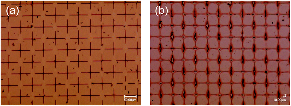
Aqueous solutions of 0.5 wt% PVA containing (5–7) × 10−4 wt% acrylic resin (PVA-based solution) were dropped over a 500-count screen mesh on a hydrophilic glass substrate and dried for 1 h at room temperature. The role of the acrylic resin additive is explained later. The removal of the mesh yielded a grid pattern of the polymer, as shown in Fig. 1(a). It was a grid line with a width of 3 μm and a height of 2.5 μm, with a diamond-shaped pattern at every other crossing point. The pattern formation mechanism is essentially the same as in a previous report,25 where a hydrophobic polymer was deposited on a glass substrate using a screen mesh. First, a drop of solution could penetrate along the mesh wire frame via capillary action (Fig. 2(1)). Then, evaporation of the solvent collects the concentrated solution at the contact points between the screen mesh and the glass surface, forming pendular rings together with liquid bridges between the neighbors (Fig. 2(2)). As the drying proceeds further, the polymer is solidified, which depends on the concentration and reflects the drying history (Fig. 2(3)). When the solution was diluted 10 times with water, a grid pattern with a narrower line of 1 μm was obtained (Fig. 1(b)). This indicates that although the solution movement could be the same as that described earlier, the polymer should be solidified at the final stage, where liquid bridges were nearly breaking because of the lower initial concentration. The narrow linewidth suggests that the liquid bridge could be stable, even at the final stage of the drying. This may be because PVA can serve as a surfactant to stabilize the interface, similar to a soap bubble, to prevent rupture even at the final stage of drying.26 A further 10 times dilution gave only dotted patterns without linking the lines (Fig. 1(c)). This means that eventually, the liquid was collected at the contact point of the mesh on the glass after the liquid bridges were broken, which is in a good agreement with our previous observation.25 When no acrylic resin was mixed, part of the diamond pattern was torn off the glass. Because the dried PVA was brittle due to its crystallinity, the contact point of the mesh on the glass where a strong force was applied was broken. The acrylic resin additive can work as an inhibiter for crystallization. In addition, we think that the additive can partially promote cross-linking of the PVA, thereby making it more difficult to wash away with H2O. Indeed, the partial PVA cross-linking was confirmed by a gel permeation chromatography analysis to compare the molecular weight distributions before and after the addition of the acrylic resin into the PVA solution (Fig. 1S†).
 |
| | Fig. 1 Optical microscopy images of PVA-based polymers on a glass fabricated through a screen mesh using aqueous solutions containing different concentrations of PVA: (a) 0.5 wt%, (b) 0.05 wt%, and (c) 0.005 wt%. | |
 |
| | Fig. 2 Schematic viewgraphs of a possible mechanism for the PVA pattern formation through a screen mesh. | |
Grid pattern formation of PVA on a sputtered Cu film
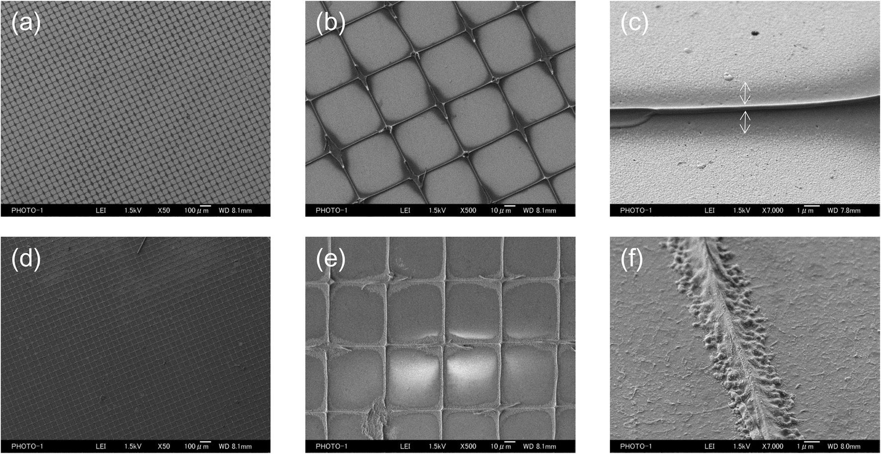
We then attempted to form the grid polymer pattern on a Cu sputtered film on a PEN substrate using a 0.5 wt% PVA-based solution, which gave a narrow, stable grid line on the glass. However, after removal of the screen mesh, the cross points of the polymer pattern, which could bind between the substrate and the screen mesh, disappeared (Fig. 3(a)). We thought that this was because of the difference between the surface properties of the Cu and glass substrates. Indeed, the contact angles were different between them. The cleaned glass substrate had a contact angle of <20°, whereas that for the as sputtered Cu surface was approximately 60°, probably owing to contaminations from the air. Therefore, the Cu surface was exposed to an alkali based solution containing a surfactant to remove them, resulting in a contact angle of <20°. The surfactant can also form a self-assembled layer on top of the cleaned Cu surface to enhance the wettability. The treatment worked quite well, yielding a grid pattern with a large area without significant defects, as shown in Fig. 3(b). This indicates that the adhesiveness of the PVA-based polymer patterns might be related to the surface hydrophilicity. Fig. 4(a)–(c) show SEM images of a PVA pattern on a Cu/PEN film. Essentially, the pattern is almost the same as that on a glass, as shown above. Examining the lines more closely, the difference in contrast between the PVA and the Cu surface in the SEM images could provide information about the structure. The PVA line fabricated through the liquid bridges between pendular rings as shown in Fig. 4(c) can be separated into two components: (1) a tube-shaped structure with a width of 0.25 μm in the middle and (2) a thin layer like bleeding extended approximately 1.75 μm from the edge of the tube at both sides (indicated by arrows in the figure). This suggested that the liquid bride maintained a homogeneous, stable line even after the solution reached the concentration where the PVA came out. This can be partially explained by the slow evaporation of water during drying, so as to give the polymer sufficient time to diffuse into the interior of the liquid line.27
 |
| | Fig. 3 Optical microscopy images of PVA-based polymers on Cu sputtered PEN film fabricated through a screen mesh using aqueous solutions containing 0.5 wt% of PVA, (a) without and (b) with the Cu surface cleaning. | |
 |
| | Fig. 4 SEM images of sputtered Cu surfaces before (a–c) and after (d–f) etched using a 0.01 M FeCl3 methanolic solution. | |
Cu etching with FeCl3
For Cu etching, the Cu film with a PVA-grid pattern deposited was dipped into the Cu etchant comprising 0.01 M FeCl3 methanolic solution, at room temperature. We used methanol instead of the more commonly used water as the solvent, because water would remove the PVA patterning from the surface, resulting in no Cu pattern left after etching. The etching time was 5–6 min to obtain transparent grid electrodes. This wet etching of Cu could proceed isotropically because the etchant was only gently stirred, so that the mass transportation of Fe3+ relied on the random diffusion in the vicinity of the Cu surface. Cross-sectional images of the Cu films were obtained during etching, as shown in Fig. 5. In order to make the insulating PVA layer visible in the images, a thin Au layer was deposited by a simple sputtering process before SEM observation. Therefore, the dark areas in between the top Au layer and the Cu surface should be occupied mainly by PVA in the images. This is corroborated by the fact that the widths of the PVA (approximately 4 μm) are consistent with those in the top view image of the PVA line in Fig. 4(c). It can be seen that the PVA layer could stick to the Cu surface throughout the process. The 6 min etching process yielded Cu grid lines with a width of 3 μm and a height of 0.8 μm together with the PVA coating on all the exposed Cu surfaces (Fig. 4(f) and 5(c)). Surprisingly, the Cu height decreased from 1.2 μm to 0.8 μm after etching. We assume that this could be occurred by the penetration of Fe3+ through the PVA film for two reasons. Firstly, there is a dependence of the etching rate on the PVA film thickness. More aggressive Cu etching through a spin-coated PVA (thickness: about 200 nm vs. ca. 1 μm for the grid electrode) was observed. The Cu height under the PVA film became from 1.4 μm to 0.4 μm when the bare Cu region was etched away. Secondly, there is no detached PVA film on the surface. The etching could proceed by the penetration of Fe3+ into the PVA layer to contact with the top of the Cu surface, rather than the penetration into the interface between the PVA film and the Cu surface from the edge. As for the undercut, it can also be mitigated by the PVA coating effect on the side, considering the long width as well as the square shape of the side wall of the Cu grid line. The undercut of the Cu did not proceed at the same rate as that of the bare Cu area (75 vs. 120 mm min−1) assuming that the PVA layer expanded to cover 4.5 μm of the length. The undercut through the isotropic etching often causes a trapezoidal shape of the metal under the resist, because the closer the metal is to the resist, the more etchant can access the metal earlier. After the etching, the surface was sufficiently cleaned with methanol. There was no significant signal due to Cl on the exposed PEN area, according to the SEM-EDS analysis (Fig. 2S†). This indicates that the etched Cu attained a form capable of being dissolved in methanol, such as CuCl2 rather than CuCl, although no additional Cl source such as HCl was added.28 A very small signal of Cl and Fe was observed in the Cu line covered with PVA patterns (Fig. 3S†). XPS spectra in the Fe (2p) region showed a small signal due to Fe(III) in the PVA coated Cu area (Fig. 2S†). This might be a trace revealing some FeCl3 penetration into the PVA resist. A Cu grid transparent electrode (6 cm × 10 cm) is shown in Fig. 4S.† A 5–6 min of etching time for the Cu thin films (thickness: 1–1.2 μm) on PEN substrates yielded a sheet resistance of 6.1 ± 5.3 Ω □−1 and transmittance of 87.2 ± 5.2%, averaged over 24 samples. Although there are some large deviations, the averaged parameters surpassed those of the conventional ITO (transmittance at 550 nm: 83%, and sheet resistance: 10 Ω □−1) in general. Because PVA is well known as a packaging polymer to prevent oxygen transmittance,29,30 we examined the effect of the PVA film over the etched Cu in terms of oxidation resistance.
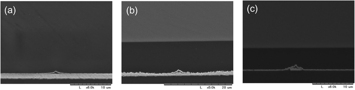 |
| | Fig. 5 Cross-sectional SEM images of Cu on PEN after (a) 0 min, (b) 3 min, and (c) 6 min etching. | |
For comparison, etched Cu samples without PVA were prepared: the PVA was removed by soaking the etched Cu in water for 5 h. The etched Cu samples with and without PVA coating were heated up to 150 °C to observe their oxidation resistance. As a result, the electric resistance of the sample without PVA increased significantly after 100 min, whereas that of the sample with PVA did not change much, even after 230 min (Fig. 6). This shows that the PVA almost completely covered the etched Cu surface to prevent oxidation. At 200 °C for less than 60 min the grid electrode without PVA became an insulator, whereas that with the polymer did not change significantly. X-ray photoelectron spectroscopy (XPS) results showed that the surface of the no-PVA Cu electrode was completely oxidized, whereas the PVA-covered Cu surface had the same XPS signals as before the heat treatment (Fig. 5S†). These results revealed that the PVA-coated Cu surface has high oxidation resistance.
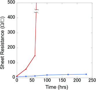 |
| | Fig. 6 Sheet resistance changes for grid Cu electrodes with (○) and without (△) PVA upon heating at 150 °C in the atmosphere as a function of time. | |
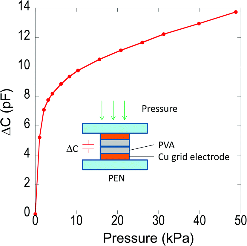
Finally, we applied the PVA-coated Cu grid electrodes for a capacitor sensor sensing pressure as a preliminary experiment. Basically, the whole sensor was fabricated just by putting two grid electrodes together so as to contact the both of PVA top layers as shown in the inset of Fig. 7. The PVA layers can serve as insulating layers. Therefore, the sensor is expected to detect the magnitude of the applied pressure by measuring the capacitance change (ΔC) generated in Cu/PVA/Cu stacked layers. Fig. 7 shows the capacitance changes as a function of applied pressure. For the pressures below 10 kPa, ΔC increases rapidly while ΔC increases in a gradually linear fashion for the pressures over 10 kPa. This result reveals that the PVA layers on Cu electrodes can work quite well as the insulating layer for the capacitor sensor.
 |
| | Fig. 7 Capacitance changes of the sensor made of grid Cu electrodes as a function of applied pressure. | |
Conclusions
A simple method to form a grid-pattern protecting layer on a Cu thin film was developed in order to obtain a transparent grid pattern by wet etching. It essentially relied on a capillary force generated between a screen mesh and the substrate when an aqueous solution containing a PVA-based polymer was introduced. The liquid bridges formed between the contacting points of the mesh and the substrate were stable enough to yield a fine-line network of solidified PVA-based polymers. A wet-etching process using FeCl3 proceeded isotropically to obtain a Cu-grid pattern thoroughly coated in the PVA-based polymer. The resulting Cu grid electrode showed good transparency and sufficiently low resistance. The PVA-based polymer coating on the Cu grid pattern efficiently protected from the Cu oxidation. This can be a good passivation to avoid decrease in the transparency due to filling all the surfaces with a passivation layer and their degradation. A preliminary result demonstrated that the PVA-coated electrode could work as a capacitor sensor sensing pressure.
Our method can be applied for nonflat surfaces, such as a cylindrical surface, because the screen mesh template is so flexible as to be easily conformable with the required surface.
Conflicts of interest
There are no conflicts to declare.
Acknowledgements
A part of this work was conducted at Tsukuba West and the Nano Processing Facility (NPF) of AIST.
References
- X. Wang, L. Zhi, N. Tsao, Ž. Tomović, J. Li and K. Müllen, Angew. Chem., Int. Ed., 2008, 47, 2990–2992 Search PubMed.
- J. Zou, H.-L. Yip, S. K. Hau and A. K.-Y. Jen, Appl. Phys. Lett., 2010, 96, 203301 Search PubMed.
- G. Gu, V. B. A. P. E. Burrows, S. R. Forrest and M. E. Thompson, Appl. Phys. Lett., 1996, 68, 2606–2608 Search PubMed.
- K. Han-Ki, D. G. Kim, K. S. Lee, M. S. Huh, S. H. Jeong, K. I. Kim and S. Tae-Yeon, Appl. Phys. Lett., 2005, 86, 183503 Search PubMed.
- M. J. Kim, D. W. Shin, J.-Y. Kim, S. H. Park, I. t. Han and J. B. Yoo, Carbon, 2009, 47, 3461–3465 CrossRef CAS.
- P. Blake, P. D. Brimicombe, R. R. Nair, T. J. Booth, D. Jiang, F. Schedin, L. A. Ponomarenko, S. V. Morozov, H. F. Gleeson, E. W. Hill, A. K. Geim and K. S. Novoselov, Nano Lett., 2008, 8, 1704–1708 CrossRef PubMed.
- S. Bae, H. Kim, Y. Lee, X. Xu, J.-S. Park, Y. Zheng, J. Balakrishnan, T. Lei, H. Ri Kim, Y. I. Song, Y.-J. Kim, K. S. Kim, B. Ozyilmaz, J.-H. Ahn, B. H. Hong and S. Iijima, Nat. Nanotechnol., 2010, 5, 574–578 CrossRef CAS PubMed.
- J. Wang, M. Liang, Y. Fang, T. Qiu, J. Zhang and L. Zhi, Adv. Mater., 2012, 24, 2874–2878 CrossRef CAS PubMed.
- D. S. Hecht, L. Hu and G. Irvin, Adv. Mater., 2011, 23, 1482–1513 CrossRef CAS PubMed.
- Z. Liu, J. Xu, D. Chen and G. Shen, Chem. Soc. Rev., 2015, 44, 161–192 RSC.
- F. Di Giacomo, A. Fakharuddin, R. Jose and T. M. Brown, Energy Environ. Sci., 2016, 9, 3007–3035 CAS.
- S. Ye, A. R. Rathmell, Z. Chen, I. E. Stewart and B. J. Wiley, Adv. Mater., 2014, 26, 6670–6687 CrossRef CAS PubMed.
- V. B. Nam and D. Lee, Nanomaterials, 2016, 6, 47 CrossRef PubMed.
- J. C. Yun, Adv. Funct. Mater., 2017, 27, 1606641 CrossRef.
- T. Sannicolo, M. Lagrange, A. Cabos, C. Celle, J.-P. Simonato and D. Bellet, Small, 2016, 12, 6052–6075 CrossRef CAS PubMed.
- M. Morales-Masis, S. De Wolf, R. Woods-Robinson, J. W. Ager and C. C. Ballif, Adv. Electron. Mater., 2017, 3, 1600529 CrossRef.
- H. Jin, S. Jung, J. Kim, S. Heo, J. Lim, W. Park, H. Y. Chu, F. Bien and K. Park, Sci. Rep., 2017, 7, 10854 CrossRef PubMed.
- K. Zilberberg and T. Riedl, J. Mater. Chem. A, 2016, 4, 14481–14508 CAS.
- A. R. Rathmell, S. M. Bergin, Y.-L. Hua, Z.-Y. Li and B. J. Wiley, Adv. Mater., 2010, 22, 3558–3563 CrossRef CAS PubMed.
- W.-K. Kim, S. Lee, D. Hee Lee, I. Hee Park, J. Seong Bae, T. Woo Lee, J.-Y. Kim, J. H. Park, Y. Cho, C. Cho and S.-Y. Jeong, Sci. Rep., 2015, 5, 10715 CrossRef CAS PubMed.
- J. H. Park, D. Y. Lee, Y.-H. Kim, J. K. Kim, J. H. Lee, J. H. Park, T.-W. Lee and J. H. Cho, ACS Appl. Mater. Interfaces, 2014, 6, 12380–12387 CAS.
- T. He, A. Xie, D. H. Reneker and Y. Zhu, ACS Nano, 2014, 8, 4782–4789 CrossRef CAS PubMed.
- S. Yang, I. Kymissis, E. Leland, S. Liu and S. O'Brien, J. Vac. Sci. Technol., B: Microelectron. Nanometer Struct., 2013, 31, 060603 Search PubMed.
- H. B. Huntington, Electromigration in Metals, in Diffusion in Solids, ed. A. S. Nowick and J. J. Burton, Academic Press, New York, 1975, ch. 6, pp. 303–352 Search PubMed.
- H. Tokuhisa, S. Tsukamoto, S. Morita, S. Ise, M. Tomita and N. Shirakawa, Appl. Surf. Sci., 2016, 400, 64–70 CrossRef.
- I. U. Vakarelski, J. O. Marston and S. T. Thoroddsen, Langmuir, 2013, 29, 4966–4973 CrossRef CAS PubMed.
- I. U. Vakarelski, J. W. Kwek, X. Tang, S. J. O'Shea and D. Y. C. Chan, Langmuir, 2009, 25, 13311–13314 CrossRef PubMed.
- Y. Xia, E. Kim, M. Mrksich and G. M. Whitesides, Chem. Mater., 1996, 8, 601–603 CrossRef CAS.
- M. Lim, H. Kwon, D. Kim, J. Seo, H. Han and S. B. Khan, Prog. Org. Coat., 2015, 85, 68–75 CrossRef CAS.
- M. Lim, D. Kim and J. Seo, Polym. Int., 2016, 65, 400–406 CrossRef CAS.
Footnote |
| † Electronic supplementary information (ESI) available. See DOI: 10.1039/c7ra11966f |
|
| This journal is © The Royal Society of Chemistry 2018 |
Click here to see how this site uses Cookies. View our privacy policy here. 
 Open Access Article
 This Open Access Article is licensed under a Creative Commons Attribution-Non Commercial 3.0 Unported Licence
 *,
S. Tsukamoto,
T. Nobeshima and
N. Yamamoto
*,
S. Tsukamoto,
T. Nobeshima and
N. Yamamoto