
 Open Access Article
 This Open Access Article is licensed under a
 Creative Commons Attribution 3.0 Unported Licence
A CH3NH3PbI3 film for a room-temperature NO2 gas sensor with quick response and high selectivity†
Xianwei Fua,
Shilong Jiaoa,
Ning Donga,
Gang Lian *a,
Tianyu Zhaoa,
Song Lva,
Qilong Wangb and
Deliang Cui*a
*a,
Tianyu Zhaoa,
Song Lva,
Qilong Wangb and
Deliang Cui*a
aState Key Lab of Crystal Materials, Shandong University, Jinan 250100, P.R. China. E-mail: liangang@sdu.edu.cn; cuidl@sdu.edu.cn
bKey Laboratory for Special Functional Aggregated Materials of Education Ministry, School of Chemistry & Chemical Engineering, Shandong University, Jinan 250100, P.R. China
First published on 2nd January 2018
Abstract
A room-temperature NO2 gas sensor with excellent performances is fabricated using an MAPbI3 (MA = CH3NH3+) thin film. It presents a high response even under extremely low NO2 concentrations. Its average response and recovery times are only ∼5 s and ∼25 s at room temperature, respectively, exhibiting its quick-responsive character. In addition, the MAPbI3-based NO2 sensor exhibits good selectivity. Interestingly, the sensitivity of the MAPbI3-based NO2 sensor is strikingly improved under high-pressure gas conditions. This phenomenon can be used for the online monitoring of chemical reaction processes and in situ detection of trace-level gas impurities under high-pressure conditions. Furthermore, based on theoretical calculations, a simple model is proposed to illustrate the corresponding gas-sensing mechanism.
1. Introduction
In modern industrialized society, the emission of harmful gases has increased substantially. Toxic gases are hazardous to human health and extremely dangerous air pollutants, among which NO2 is one of the most common harmful gases. The increasing concern for protecting the environment and biological systems has resulted in continuous endeavors in improving gas sensors.1–4 To date, many types of inorganic and organic compounds have been utilized as sensing materials.5,6 Although traditional metal oxides generally present high responses, they have an obvious disadvantage, which is the high working temperatures. For example, although CuO plates showed high sensitivity to NO2, the optimum operating temperature was 200 °C.7 A ZnO nanowire sensor exhibited high sensitivity and fast response to ethanol gas at a temperature as high as 300 °C.8 WO3 was believed to be a promising material for NO2 gas sensor, but it was typically used in the temperature range from 200 °C to 350 °C.9,10 This disadvantage severely limits their further applications in the field of gas sensors. To achieve the requirement of a low optimum working temperature, some organic compounds have been used as low-temperature gas sensing materials. However, quick response and recovery speed are other challenging issues for organic gas sensors. For instance, the response and recovery time of a lead phthalocyanine (PbPc) film sensor were about hundreds of seconds for NO2.11 The gas sensing behaviors of tetra-(tert-butyl) phthalocyanine copper (CuPc(t-Bu)4) films were investigated at room temperature, but their response and recovery speed were very slow.12 Therefore, based on the advantage of the low working temperature of organic gas sensors, how to greatly improve the response and recovery speed has been a great challenge to date.Organometallic halide perovskites MAPbX3 (X = Cl, Br, I) have attracted much attention due to their interesting and intriguing properties, including moderate bandgaps, large optical absorption coefficients,13,14 extraordinarily long carrier diffusion lengths and high carrier mobilities.15,16 They present some extensive applications in solar cells, light emitting diodes (LEDs),17 photodetectors,18 sensors,19 field effect transistors (FETs),20 lasers21 and so on. As a typical bipolar charge transport semiconductor,22 the electrical conductivity of MAPbX3 is greatly influenced by some oxidizing and reducing gases. For instance, ammonium gas could induce a quick reversible phase transformation in a perovskite film, resulting in an obvious decrease in its resistance.23,24 MAPbI3 was also sensitive to some polar organic compounds, such as 4-tert-butylpyridine25 and acetonitrile.26 MAPbI3−xClx films could absorb many types of gases, e.g. NO2, SO2, alcohol and acetone, which caused obvious changes in their conductivity.27 In addition, the resistance of an MAPbI3−xClx thin film also exhibited a quick reversible decrease in the presence of moisture. These quick room-temperature reversible behaviors of perovskite films indicate their potential application in the field of gas sensors. Thus, MAPbX3-based gas sensors with low working temperatures, and quick responses and recovery speeds can be expected. However, most research groups have focused on the photoelectric fields of MAPbI3−xClx and a few investigations have been reported on MAPbX3-based gas sensors. Furthermore, because the stability of organic–inorganic hybrid semiconductors is strikingly improved under a high-pressure atmosphere,28 it would be quite interesting to investigate the response performance of stabilized perovskite films to target gases under high pressure.
Herein, we prepare MAPbI3 thin film gas sensors and investigate their gas-sensing properties under both ambient and high pressure. Interestingly, the gas sensors exhibit rather quick responses and recovery speeds, excellent selectivity and high sensitivity to NO2 gas even at room temperature. Furthermore, the sensitivity of the prepared sensor is strikingly improved under high-pressure gas. Additionally, theoretical simulation of the adsorption of NO2 molecules on the surface of perovskite is conducted to illustrate the response mechanism of the sensor.
2. Experimental
2.1 Preparation of perovskite thin film and gas sensor devices
In a typical process, 1 mmol of methylammonium iodide (MAI, AR, Tokyo Chemical Industry Co., Ltd, Tokyo, Japan) and 1 mmol of PbI2 (AR, Aladdin Industrial Corporation, Shanghai, China) were successively dissolved in 1 mL N,N-dimethyl formamide (DMF, AR, Sinopharm Chemical Reagent Co., Ltd, China) at 65 °C under stirring for 12 h.29,30 Afterwards, the precursor solution was spin-coated on an alumina (Al2O3) ceramic substrate (10 × 14 mm) at 1500 rpm for 9 s, followed by spinning at 2000 rpm for another 10 s. The film was then dried under high purity argon gas at 100 °C for 30 min. Finally, gold interdigital electrodes were sputter-coated on the perovskite film (Fig. S1†). Then, the gas sensor was prepared for further characterization.2.2 Characterization of samples
Fourier transformation infrared (FTIR) absorption spectra were collected on a Thermo-Nicolet NEXUS 670 infrared spectrometer using the attenuated total reflection (ATR) mode, and the wavenumber resolution was 4 cm−1 (range 4000–650 cm−1). X-ray diffraction (XRD) patterns were recorded on a Bruker-AXS D8 Advance X-ray diffractometer with CuKα radiation (λ = 1.54186 Å) in the 2θ range of 10–60°. The morphology was observed via scanning electron microscopy (SEM, Hitachi S-4800) and scanning probe microscopy (SPM, Veeco Instruments Inc, Dimension Icon). The transient gas response characteristics (I–t curves) of the gas sensors were examined using a Keithley 4200-SCS semiconductor parameter analyzer at room temperature (25 ± 3 °C) in a specially designed gas cabinet with a volume of 180 mL, and the relative humidity was 25–30%.The high-pressure and atmosphere pressure gas-sensing performances of the sensors were examined using a specially designed chamber with a capacity of 180 mL (Fig. S2†), which was connected to the Keithley 4200-SCS semiconductor parameter analyzer. Before characterization, the air in the chamber was completely expelled with high-purity argon gas. Afterwards, a specific volume of target gas was stored in the target gas cylinder which was connected to the chamber. When the pressure inside the chamber was increased to designated pressures (1, 2, 3, 4, 5, 6, 7 and 8 MPa) by introducing high-pressure argon gas, the target gas stored in the cylinder was injected into the testing chamber. The variation in the resistance of the sensors was recorded simultaneously. When the measuring process was finished, the high-pressure gas was released from the chamber, which carries away the target gases. Then the resistance of the sensor recovered to its original value. Details of the operation process are presented in ESI Fig. S3.†
For oxidizing gases, we define the response R of a gas sensor as:
 | (1) |
 | (2) |
For both oxidizing and reducing gases, the sensitivity S is defined as:
 | (3) |
2.3 Theoretical calculation
To explain the gas-sensing experimental results, molecular dynamics simulation was conducted using the FORCITE package in the Materials Studio. The COMPASS (Condensed-phase Optimized Molecular Potentials for Atomistic Simulation Studies)31,32 force-field was performed to describe the interaction between NO2 and the surface atoms of perovskite. For the case in which NO2 interacted with perovskite, the (110) surface was created by periodical replication of an elementary cell in both x and y directions, where the periodical condition was applied. The thickness of the vacuum slab was set to be 15 Å in order to avoid unnecessary interactions between adjacent layers. The NVT ensemble with a simulation time of 5 ns was used to run the test, and the step was maintained at 1 fs.3. Results and discussion
Initially, the phase composition of the film was identified via XRD. In Fig. 1a, the peaks at 14.1, 28.4, 31.9 and 43.2° can be indexed to the (110), (220), (310) and (314) planes of tetragonal MAPbI3, respectively,33 while the other peaks originate from the Al2O3 substrate (JCPDS no. 46-1212). It was reported that the porous morphology plays an important role in the gas-sensing performance of a gas sensor.34 Fig. 1b presents the surface morphology of the MAPbI3 film, which was constructed by interconnected MAPbI3 nanoplates. The film has a large number of pores, which is also supported by the cross-section image (Fig. S4†). The MAPbI3 nanoplates were also measured via TEM (Fig. S5†). Furthermore, the height profile of the film recorded with AFM (within an area of 20 × 20 μm2, Fig. 1c and d) reveals a rough surface with a root mean square roughness (MRS) of ∼125 nm. This structural characteristic provides plentiful diffusion channels and active surface sites for the target gas molecules. Thus, a good gas-sensing performance can be anticipated.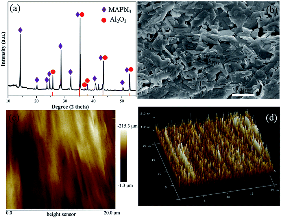 | ||
| Fig. 1 Characterization of the prepared MAPbI3 film. (a) XRD pattern, (b) SEM image and (c and d) AFM morphology profiles. | ||
Furthermore, the gas-sensing performance of the MAPbI3 film to NO2 gas at different concentrations was tested. The sensor response was then calculated using eqn (1), as plotted in Fig. 2. When NO2 gas was injected into the testing chamber, the resistance of the film sensor with NO2 adsorbed obviously decreased. This tendency was more prominent at higher concentrations of NO2 (Fig. 2a). The inset reveals an almost linear relationship between the sensor response and the concentration of NO2, and the average sensitivity was as high as 0.62 ppm−1 (Fig. 2a). Besides, the dynamic response curves and sensor response vs. NO2 concentration under different bias voltages are shown in Fig. S6.† The signal-to-noise ratio slightly increased with the improvement in bias voltage. More importantly, the detection concentration of NO2 gas was as low as 1 ppm, and a clear response was still presented (Fig. 2a and S6†). An extremely low detection limit of the MAPbI3 film sensor, which indicates rather high sensitivity at room temperature, could be undoubtedly expected. More interestingly, the room-temperature sensing performance of the MAPbI3 film sensor for NO2 strikingly surpassed the high-temperature performance of most conventional metal oxide sensors (Table 1).19,35–40 Compared to the room-temperature CuTAP(t-Bu)4 film sensors, the gas-sensing performance of the prepared MAPbI3 film is also superior (Table 1). In addition, the response–recovery curve of the film (Fig. 2b) exhibits a much quicker response and recovery speed than MAPbI3−x(SCN)x film sensors at room temperature. The average response and recovery times were ∼5 s and ∼25 s, respectively, which are preponderant for a room-temperature gas sensor.
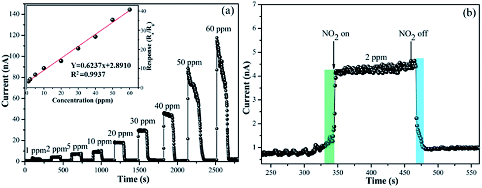 | ||
| Fig. 2 (a) Dynamic response curves of the MAPbI3 film sensor recorded in different concentrations NO2 (1–60 ppm), inset shows the response of the MAPbI3 film sensor vs. concentration of NO2. (b) Response and recovery processes in 2 ppm NO2. All the curves were recorded at room-temperature under a bias-voltage of 10 V. | ||
| Structure | Operating temperature | NO2 concentration (ppm) | Sensitivity | Response time (s) | Recovery time (s) | Detection of target gases | Ref |
|---|---|---|---|---|---|---|---|
| In2O3 nanowires | 250 °C | 1 | 2.57 | 20 | 40 | NO2 | 35 |
| SnO2–ZnO/polyaniline | 180 °C | 35 | 368.9 | 9 | 27 | NO2 | 36 |
| P3HT–SnO2 composite | 100 °C | 30 | 55 | 50 | 30 | NO2 | 37 |
| CuTAP(t-Bu)4 films | Room temperature | 50 | 5 | 270 | 540 | NO2 | 38 |
| ZnO-nanowire | 225 °C | 0.5 | 15 | 24 | 12 | NO2 | 39 |
| WO3 nanoplates | 100 °C | 5 | 10 | 50 | 500 | NO2 | 40 |
| MAPbI3−x(SCN)x | Room temperature | 0.2 | 3 | 222 | 360 | NO2 | 19 |
| Our work | Room temperature | 1 | 3.3 | 22 | 13 | NO2 |
Besides the sensor response, reproducibility and selectivity are also crucial for gas sensors. In order to investigate the reproducibility of the MAPbI3 film gas sensor, NO2 was repeatedly injected into and evacuated from the testing chamber. The sensor response of the film remained stable after more than 12 cycles (Fig. 3a). For comparison, the reproducibility of the MAPbI3 film sensor in ambient environment with a relative humidity of 35% was also examined (Fig. S7†). Compared with the situation in Ar atmosphere, although the current of this sensor slightly decreased, it still retained good stability after four cycles. To examine the selectivity of the sensor, NO2 (1% NO2 in Ar), SO2 (1% SO2 in Ar), HCHO (1% HCHO in Ar), CH4, CO, NH3 (1% NH3 in Ar), (CH3)3N, O2 (21% O2 in Ar) and H2O were selected as reference gases. According to the definition of sensitivity (eqn (3)), we calculated the sensitivities of the MAPbI3 film sensor to the abovementioned gases, which are presented in Fig. 3b. The sensitivity of the MAPbI3 film sensor to NO2 was 0.67 ppm−1, whereas that for the reference gases were rather low, such as 0.016 ppm−1 for SO2, 0.011 ppm−1 for NH3, 0.034 ppm−1 for HCHO, 0.0001 ppm−1 for CH4, 0.0001 ppm−1 for CO, 0.00005 ppm−1 for (CH3)3N, 0.0042 ppm−1 for H2O and 0.0001 ppm−1 for O2. The dynamic response and recovery curves are shown Fig. S8.† The MAPbI3 film sensor response to the reference gases was in striking contrast with its response to NO2, except for H2O and O2. The resistance increased when the reference gases were injected into the testing chamber. This characteristic caused the MAPbI3 film sensor to quite easily distinguish NO2 from the other gases.
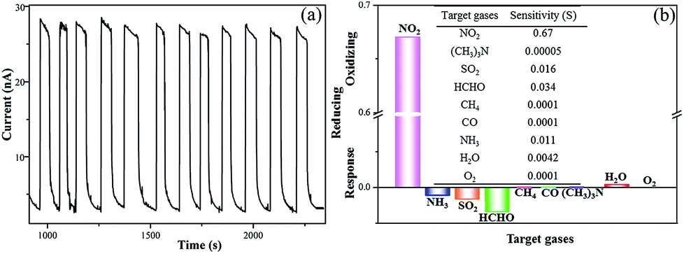 | ||
| Fig. 3 (a) Reproducibility of the MAPbI3 sensor exposed to 30 ppm NO2 and (b) sensitivity to a series reference gases. | ||
In order to analyze the gas-sensing mechanism, in situ FTIR measurements of the MAPbI3 film exposed to NO2 gas for different durations were conducted. The obtained spectrum (Fig. 4a) is in good accordance with the reported result.41 The bands at 3091, 2819, 1659, 1487, 1416, 1244 and 902 cm−1 are attributed to the N–H stretch, C–H stretch, N–H bend, C–H bend, C–N stretch, C–H twist and C–H rock vibration modes, respectively.42 It was worth noting that a new band appeared at 1325 cm−1 (Fig. 4b), which can be assigned to the surface bound NO2− ions formed by charge transfer chemisorption.43,44 When the film was exposed to NO2 for a longer time, more gas molecules were adsorbed on the active sites in the porous film. Therefore, this new band became stronger (Fig. 4c). The electron transfer process is also supported by the red-shift of the N–H stretching vibration band from 3091 cm−1 to 3076 cm−1. The corresponding increase in hole concentration of the P-type MAPbI3 film led to the resistance decreasing in the electrical field.
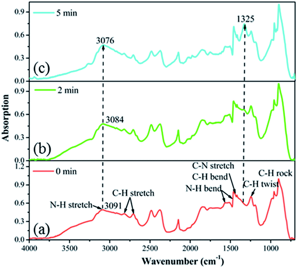 | ||
| Fig. 4 FTIR spectra of the MAPbI3 film sensor exposed to 1% NO2 for different durations. | ||
The interaction between the adsorbed NO2 molecules and MAPbI3 film was further investigated via computational simulations. Fig. 5a–c show the radial distribution functions (RDFs) of NO2–HMA+ on the typical (110) facet of perovskite, where, HMA+ includes two types of –CH3 and –NH3. The peaks at 2.50 Å and 2.63 Å (Fig. 5a) reveal a stronger hydrogen-bond interaction between –CH3 and NO2, compared to that between –NH3 and NO2 (the peaks at 3.53 Å and 2.94 Å, respectively (Fig. 5b)). This result is consistent with that of FTIR spectra quite well. Subsequently, a schematic illustrating the electron transfer process from perovskite to the NO2 molecule via the hydrogen-bond channel was proposed (Fig. 5c). According to the FTIR spectra and theoretical simulation results, the adsorbed NO2 molecules first interact with the –CH3 groups and then attract some electrons from the organic components. In fact, the inorganic Pb–I skeleton in the perovskite semiconductor serves as the major transportation path for the charge carriers.45 Thus some electrons on the Pb–I skeleton subsequently transfer to MA+ ions via the NH⋯I bonds (Fig. 5c). As a result, the hole concentration of the perovskite film is enhanced, leading to a striking decrease in the resistance of the film.
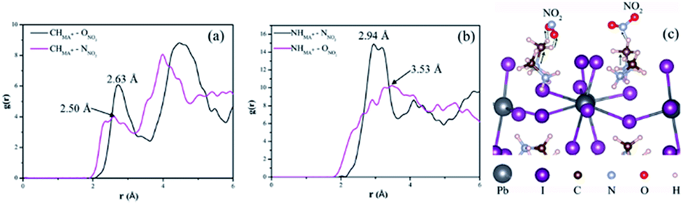 | ||
| Fig. 5 (a and b) Radial distribution functions of adsorbed NO2 molecules on the (110) face of MAPbI3. (c) Proposed model to explain the gas-sensing process of the perovskite film sensor to NO2 gas. | ||
In addition, based on the theoretical calculation (Fig. S9†), the interaction between the NO2 molecules and perovskite film is enhanced with the improvement in gas pressure due to the increase in adsorption energy. Consequently, more effective electron transfer can be expected between them under a high-pressure circumstance, which plays an important role in the excellent performance of this sensor. Therefore, the effect of pressure on the gas-sensing performance was investigated. In our experiments, V, R and T are all constants, thus the molar number of argon gas n is simply proportional to the pressure p. According to the ideal gas equation, n = p/p0 × n0 (where, n0 is the molar number of argon gas at atmospheric pressure and p0 is atmospheric pressure). Besides, the molar number of target gases nt is much less than n (Fig. S10†), thus the molecule number concentration of target gases at high pressure ct can be expressed as:
 | (4) |
According to the way that we ignore the molar number of target gases, the error was determined to be only 0.005‰ (Fig. S10†), thus this approach is feasible.
Fig. 6a shows the dynamic response of the MAPbI3 film sensor to NO2 gas at high pressures, where the molecule number concentration of NO2 remains constant for all the pressures, namely, 5 ppm. Obviously, the sensor response strikingly increased in a near-linear way with an increase in pressure, and the MAPbI3 film sensor still exhibited rather quick response and recovery times of 11–25 s and 20–60 s under high pressure. According to eqn (3) and (4), we calculated the sensitivity of the MAPbI3 film sensor under high pressure, and the results are presented in the inset in Fig. 6a. Interestingly, the sensitivity of the MAPbI3 film sensor strikingly increased under high pressure, which should be closely related with the fact that the adsorption energy of the NO2 molecules on the surface of the sensor increased (Fig. S9†) and more NO2 molecules were strongly absorbed the surface of MAPbI3 film under higher pressure,46 resulting in more effective electron transfer and an increase in hole concentration. Actually, in the ideal gas model, the adsorption of gas molecules is not only determined by the adsorption energy, but also depends on the partial pressure of the target gas. Therefore, the positive effect of the partial pressure of NO2 cannot be ignored for the enhanced sensitivity. Besides, the MAPbI3 film sensor still exhibited quite high selectivity towards NO2 even at high pressure (Fig. S11†). This phenomenon has potential applications in improving the performance of gas sensors when detecting ultra-low concentrations of target gases.
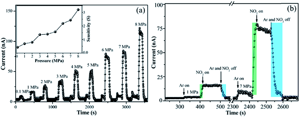 | ||
| Fig. 6 (a) Dynamic response curve of the MAPbI3 film sensor recorded in NO2 with the same molecule number concentration at different pressures, inset shows the sensitivity of the MAPbI3 film sensor vs. pressure under the same molecule number concentration of NO2. (b) Transient curve when high-pressure argon gas and NO2 are successively introduced into the testing chamber at 1 and 7 MPa. All the curves were recorded at room-temperature under a bias-voltage of 10 V. | ||
4. Conclusions
By utilizing an organic–inorganic hybrid semiconductor, a gas sensor with strikingly improved sensitivity and rather quick response and recovery speed was prepared at room temperature. Furthermore, the sensitivity of the gas sensor was greatly increased under high-pressure argon gas, providing the possibility of enabling the sensor to detect target gases with ultra-low concentrations by applying a high-pressure. These findings may provide a new route for the fabrication of ultra-sensitive gas sensors for the on-line monitoring of chemical reaction processes and in situ analyzing impurity gases under high-pressure circumstances.Conflicts of interest
There are no conflicts to declare.Acknowledgements
This work was supported by the Natural Science Foundation of China (NSFC 51372143, 51102151) and Natural Science Foundation of Shandong Province (ZR2011EMQ002).References
- D. Zhang, J. Liu, H. Chang, A. Liu and B. Xia, RSC Adv., 2015, 5, 18666–18672 RSC.
- D. Zhang, J. Wu, P. Li and Y. Cao, J. Mater. Chem. A, 2017, 5, 20666–20677 CAS.
- A. T. Mane, S. T. Navale and V. B. Patil, Org. Electron., 2015, 19, 15–25 CrossRef CAS.
- S. T. Navale, G. D. Khuspe, M. A. Chougule and V. B. Patil, Ceram. Int., 2014, 40, 8013–8020 CrossRef CAS.
- A. R. Jalil, H. Chang, V. K. Bandari, P. Robaschik, J. Zhang, P. F. Siles, G. Li, D. Bürger, D. Grimm, X. Liu, G. Salvan, D. R. T. Zahn, F. Zhu, H. Wang, D. Yan and O. G. Schmidt, Adv. Mater., 2016, 28, 2971–2977 CrossRef CAS PubMed.
- S. Capone, M. Benkovicova, A. Forleo, M. Jergel, M. G. Manera, P. Siffalovic, A. Taurino, E. Majkova, P. Siciliano, I. Vavra, S. Luby and R. Rella, Sens. Actuators, B, 2017, 243, 895–903 CrossRef CAS.
- Y. Li, J. Liang, Z. Tao and J. Chen, Mater. Res. Bull., 2008, 43, 2380–2385 CrossRef CAS.
- Q. Wan, Q. H. Li, Y. J. Chen, T. H. Wang, X. L. He, J. P. Li and C. L. Lin, Appl. Phys. Lett., 2004, 84, 3654–3656 CrossRef CAS.
- T. Kida, A. Nishiyama, M. Yuasa, K. Shimanoe and N. Yamazoe, Sens. Actuators, B, 2009, 135, 568–574 CrossRef CAS.
- C. Cantalini, H. T. Sun, M. Faccio, M. Pelino, S. Santucci, L. Lozzi and M. Passacantando, Sens. Actuators, B, 1996, 31, 81–87 CrossRef CAS.
- J. C. Hsieh, C. J. Liu and Y. H. Ju, Thin Solid Films, 1998, 322, 98–103 CrossRef CAS.
- B. Wang, X. Zuo, Y. Wu, Z. Chen, C. He and W. Duan, Sens. Actuators, B, 2011, 152, 191–195 CrossRef CAS.
- S. Sun, T. Salim, N. Mathews, M. Duchamp, C. Boothroyd, G. Xing, T. C. Sum and Y. M. Lam, Energy Environ. Sci., 2014, 7, 399–407 CAS.
- J. M. Ball, S. D. Stranks, M. T. Hörantner, S. Hüttner, W. Zhang, J. W. Crossland, I. Ramirez, M. Riede, M. B. Johnston, U. Steiner, J. Henry, E. J. W. Crossland, I. Ramirez, M. Riede, M. B. Johnston, R. H. Friend and H. J. Snaith, Energy Environ. Sci., 2015, 8, 602–609 CAS.
- F. Zhang, B. Yang, X. Mao, R. Yang, L. Jiang, Y. Li, J. Xiong, Y. Yang, R. He, W. Deng and K. Han, ACS Appl. Mater. Interfaces, 2017, 9, 14827–14832 CAS.
- Q. Dong, Y. Fang, Y. Shao, P. Mulligan, J. Qiu, L. Cao and J. Huang, Science, 2015, 347, 967–970 CrossRef CAS PubMed.
- A. B. Wong, M. Lai, S. W. Eaton, Y. Yu, E. Lin, L. Dou, A. Fu and P. Yang, Nano Lett., 2015, 15, 5519–5524 CrossRef CAS PubMed.
- G. Maculan, A. D. Sheikh, A. L. Abdelhady, M. I. Saidaminov, M. A. Haque, B. Murali, E. Alarousu, O. F. Mohammed, T. Wu and O. M. Bakr, J. Phys. Chem. Lett., 2015, 6, 3781–3786 CrossRef CAS PubMed.
- Y. Zhuang, W. Yuan, L. Qian, S. Chen and G. Shi, Phys. Chem. Chem. Phys., 2017, 19, 12876–12881 RSC.
- N. Cho, F. Li, B. Turedi, L. Sinatra, S. P. Sarmah, M. R. Parida, M. I. Saidaminov, B. Murali, V. M. Burlakov, A. Goriely, O. F. Mohammed, T. Wu and O. M. Bakr, Nat. Commun., 2016, 7, 13407 CrossRef CAS PubMed.
- G. Xing, M. H. Kumar, W. K. Chong, X. Liu, Y. Cai, H. Ding, M. Asta, M. Grätzel, S. Mhaisalkar, N. Mathews and T. C. Sum, Adv. Mater., 2016, 28, 8191–8196 CrossRef CAS PubMed.
- C. S. Ponseca, T. J. Savenije, M. Abdellah, K. Zheng, A. Yartsev, T. Pascher, T. Harlang, P. Chabera, T. Pullerits, A. Stepanov, J.-P. Wolf and V. Sundström, J. Am. Chem. Soc., 2014, 136, 5189–5192 CrossRef CAS PubMed.
- C. Bao, J. Yang, W. Zhu, X. Zhou, H. Gao, F. Li, G. Fu, T. Yu and Z. Zou, Chem. Commun., 2015, 51, 15426–15429 RSC.
- Y. Zhao and K. Zhu, Chem. Commun., 2014, 50, 1605–1607 RSC.
- W. Li, H. Dong, L. Wang, N. Li, X. Guo, J. Li and Y. Qiu, J. Mater. Chem. A, 2014, 2, 13587–13592 CAS.
- G. Niu, X. Guo and L. Wang, J. Mater. Chem. A, 2015, 3, 8970–8980 CAS.
- L. Hu, G. Shao, T. Jiang, D. Li, X. Lv, H. Wang, X. Liu, H. Song, J. Tang and H. Liu, ACS Appl. Mater. Interfaces, 2015, 7, 25113–25120 CAS.
- L. Cao, Z. Liu, T. Wang, H. Dai, L. Zhang, X. Tao and D. Cui, CrystEngComm, 2012, 14, 5795 RSC.
- Y. Zhou, H. F. Garces and N. P. Padture, Frontiers of Optoelectronics, 2016, 9, 81–86 CrossRef.
- N. Ahn, D. Y. Son, I. H. Jang, S. M. Kang, M. Choi and N. G. Park, J. Am. Chem. Soc., 2015, 137, 8696–8699 CrossRef CAS PubMed.
- H. Sun, J. Phys. Chem. B, 1998, 5647, 7338–7364 CrossRef.
- H. Sun, P. Ren and J. R. Fried, Comput. Theor. Polym. Sci., 1998, 8, 229–246 CrossRef CAS.
- Y. Zhao, A. M. Nardes and K. Zhu, Appl. Phys. Lett., 2014, 104, 213906 CrossRef.
- V. B. Raj, A. T. Nimal, M. Tomar, M. U. Sharma and V. Gupta, Sens. Actuators, B, 2015, 220, 154–161 CrossRef CAS.
- P. Xu, Z. Cheng, Q. Pan, J. Xu, Q. Xiang, W. Yu and Y. Chu, Sens. Actuators, B, 2008, 130, 802–808 CrossRef CAS.
- H. Xu, X. Chen, J. Zhang, J. Wang, B. Cao and D. Cui, Sens. Actuators, B, 2013, 176, 166–173 CrossRef CAS.
- T. Zhao, X. Fu, X. Cui, G. Lian, Y. Liu, S. Song, Q. Wang, K. Wang and D. Cui, Sens. Actuators, B, 2017, 241, 1210–1217 CrossRef CAS.
- B. Wang, X. Zuo, Y. Wu, Z. Chen, C. He and W. Duan, Sens. Actuators, B, 2011, 152, 191–195 CrossRef CAS.
- M. W. Ahn, K. S. Park, J. H. Heo, J. G. Park, D. W. Kim, K. J. Choi, J. H. Lee and S. H. Hong, Appl. Phys. Lett., 2008, 93, 263103 CrossRef.
- S. S. Shendage, V. L. Patil, S. A. Vanalakar, S. P. Patil, N. S. Harale, J. L. Bhosale, J. H. Kim and P. S. Patil, Sens. Actuators, B, 2017, 240, 426–433 CrossRef CAS.
- A. Halder, D. Choudhury, S. Ghosh, A. S. Subbiah and S. K. Sarkar, J. Phys. Chem. Lett., 2015, 6, 3180–3184 CrossRef CAS.
- P. Bhatt, K. Pandey, P. Yadav, B. Tripathi, C. K. P. Kanth, M. K. Pandey and M. Kumar, Sol. Energy Mater. Sol. Cells, 2015, 140, 320–327 CrossRef CAS.
- T. V. Basova, E. K. Kol'Tsov and I. K. Igumenov, Sens. Actuators, B, 2005, 105, 259–265 CrossRef CAS.
- A. Capobianchi, A. M. Paoletti, G. Pennesi and G. Rossi, Sens. Actuators, B, 1998, 48, 333–338 CrossRef CAS.
- Z.-J. Zhang, S.-C. Xiang, G.-C. Guo, G. Xu, M.-S. Wang, J.-P. Zou, S.-P. Guo and J.-S. Huang, Angew. Chem., Int. Ed., 2008, 47, 4149–4152 CrossRef CAS PubMed.
- S. Himeno, T. Komatsu and S. Fujita, J. Chem. Eng. Data, 2005, 50, 369–376 CrossRef CAS.
Footnote |
| † Electronic supplementary information (ESI) available. See DOI: 10.1039/c7ra11149e |
| This journal is © The Royal Society of Chemistry 2018 |