
 Open Access Article
 This Open Access Article is licensed under a Creative Commons Attribution-Non Commercial 3.0 Unported Licence
Role of annealing temperature on the sol–gel synthesis of VO2 nanowires with in situ characterization of their metal–insulator transition†
Y.-R. Jo,
S.-H. Myeong and
B.-J. Kim *
*
School of Materials Science and Engineering, Gwangju Institute of Science and Technology (GIST), 123 Cheomdangwagi-ro, Buk-gu, Gwangju, Korea. E-mail: kimbj@gist.ac.kr; Tel: +82-062-715-2341
First published on 30th January 2018
Abstract
Among the techniques to create VO2 nanostructures, the sol–gel method is the most facile and benefits from simple, manipulable synthetic parameters. Here, by utilizing various TEM techniques, we report the sequential morphological evolution of VO2 nanostructures in a sol–gel film spin-coated on a customized TEM grid, which underwent oxygen reduction as the annealing temperature increased. In situ TEM dark-field imaging and Raman spectroscopy allowed us to confirm the sharp phase transition behavior of an individual nanowire by illustrating the effect of electrode-clamping-induced tensile stress on the nucleation of the R phase from the M1 phase. The electrical transport properties of a single-nanowire device fabricated on a customized TEM grid showed excellent control of the stoichiometry and crystallinity of the wire. These results offer critical information for preparing tailored VO2 nanostructures with advanced transition properties by the sol–gel method to enable the fabrication of scalable flexible devices.
1. Introduction
The most well-known strongly correlated material, VO2, has received considerable attention for its potential applications, such as in Mott field transistors,1,2 thermochromic glazing,3 electrical-optical switching devices,4,5 memory devices,6 flat panel displays7 and lithium batteries.8 This material has been highly recognized because of its first-order metal-insulator transition (MIT), accompanied by a reversible structural phase transition from a high-temperature tetragonal rutile phase to a low-temperature monoclinic phase at a critical temperature of ∼68 °C.9,10 Although the MIT mechanism in VO2 is under intense debate, it is believed that the transition is driven by either strong electron–electron interactions (Mott transition),11,12 electron–phonon interactions (Peierls transition),13 or a combination of both.11,14,15 Moreover, the MIT properties in VO2 can be easily controlled by the stoichiometry,16–18 doping,19–21 size effects,22 external stress,23,24 and interfacial stress.10,25,26Owing to the capability of tuning the phase transition temperature and avoiding the creation of complicated multiple phases, considerable effort has been devoted to synthesizing VO2 nanostructures with specific crystal structures, morphologies, sizes, and dopants using growth methods such as vapor transport,5,27,41 sol–gel,28,29 hydrothermal synthesis,8,42,43 chemical vapor deposition,30 and pulsed laser ablation.31 Among these techniques, sol–gel is the simplest because its process can be easily controlled by parameters such as the concentration of the vanadium precursor, the solvent, the aging time and the reaction temperature, which make it desirable for large-scale, faster, cheaper, and low-temperature synthesis. Although a recent report demonstrated the successful synthesis of various morphologies and crystal structures of VO2 nanostructures using different sol–gel conditions32 such as varying precursor aging time and using secondary annealing, the role of annealing temperature in determining the morphology, stoichiometry and phase of the VO2 nanostructures remains elusive. Moreover, the MIT properties of individual nanowires, synthesized by the sol–gel method have not been inspected due to the small lengths of the wires and their tendency to aggregate during synthesis.32 Additionally, simultaneous examination of structural, chemical, and electrical properties with the identical single nanowire grown by sol–gel methods has not been carried out.
Here, exploiting a customized TEM grid with Si3N4 membranes on which a sol–gel film was spin-coated and examined using various TEM techniques, we thoroughly analyzed the temperature dependence of the aforementioned properties of VO2 nanostructures. We found that the annealing temperature is a crucial parameter to control the morphology of VO2 nanostructures via coarsening phenomenon, and it determines the stoichiometry of the vanadium oxide nanostructure via oxygen reduction: as the temperature increased (up to 550 °C), the solvent was removed, and the precursors agglomerated. Subsequently, VO2 nanoparticles were formed and then they were converted to nanowires via particle coarsening. In company with this, our nanoprobe EDS analysis interpreted the reaction mechanism by quantifying the V/O ratio and indicated that the oxygen in the film was reduced during annealing until the ratio reached to V/O = 1![[thin space (1/6-em)]](https://www.rsc.org/images/entities/char_2009.gif) :2. The sol–gel spin-coating on customized Si3N4 TEM grids with annealing allowed us to form the VO2 nanowires which were sufficiently long (up to 10 μm) and widely distributed to fabricate individual nanowire devices, and provided a platform to directly correlate the structural, chemical, and electrical properties of identical single nanowires. The phase transition characteristics of the individual nanowires were examined by in situ TEM DF imaging and Raman spectroscopy, revealing that both the electrode-free and electrode-clamped VO2 nanowires underwent abrupt phase transitions (i.e. the former occurred at 69 °C over a span of ∼0.1 °C and the latter, at 75.5 °C over a span of ∼1.0 °C) during temperature cycling, demonstrating that our sol–gel method excellently controls the stoichiometry and crystallinity of the wire. The tensile stress occurring from the latter delayed the transition temperature by slightly extending its span for M1 to R transition. In situ TEM DF allowed us to observe that this transition was initiated from multiple nucleation of the R phase to effectively relax the tensile stress resulting from electrode-clamping. Consecutively, the resistance vs. temperature plot of the electrode-clamped wire was acquired, which demonstrated the electrical band gap of the wire to be approximately 600 mV, which is consistent with the optical band gap of VO2, showing the optimized stoichiometric control and high crystallinity.
:2. The sol–gel spin-coating on customized Si3N4 TEM grids with annealing allowed us to form the VO2 nanowires which were sufficiently long (up to 10 μm) and widely distributed to fabricate individual nanowire devices, and provided a platform to directly correlate the structural, chemical, and electrical properties of identical single nanowires. The phase transition characteristics of the individual nanowires were examined by in situ TEM DF imaging and Raman spectroscopy, revealing that both the electrode-free and electrode-clamped VO2 nanowires underwent abrupt phase transitions (i.e. the former occurred at 69 °C over a span of ∼0.1 °C and the latter, at 75.5 °C over a span of ∼1.0 °C) during temperature cycling, demonstrating that our sol–gel method excellently controls the stoichiometry and crystallinity of the wire. The tensile stress occurring from the latter delayed the transition temperature by slightly extending its span for M1 to R transition. In situ TEM DF allowed us to observe that this transition was initiated from multiple nucleation of the R phase to effectively relax the tensile stress resulting from electrode-clamping. Consecutively, the resistance vs. temperature plot of the electrode-clamped wire was acquired, which demonstrated the electrical band gap of the wire to be approximately 600 mV, which is consistent with the optical band gap of VO2, showing the optimized stoichiometric control and high crystallinity.
2. Experimental section
2.1. Synthesis of VO2 nanostructures using sol–gel spin-coating
The synthetic procedure to fabricate VO2 nanostructures is described in Fig. 1. First, vanadium oxyacetylacetone (VO(acac)2, 99%, Aldrich, 0.335 g) and methanol (99.8%, Aldrich, 5 g) were ultrasonically mixed to prepare a 0.25 m precursor solution for film coating. The well-mixed precursor solution was aged in a glove box (N2, 99.999%) at room temperature for 25 days. Then, the aged precursor solution (30 μL) was dropped onto plasma-treated (50 W, 10 minutes) Si3N4 membranes (50 nm thick) on a customized transmission electron microscopy (TEM) sample grid, followed by spin-coating the solution at 3000 rpm for 20 seconds in a glove box. The spin-coating was repeated three times over the resulting layers. The coated film was dried at 80 °C for 20 minutes to evaporate the excess solvent using a hot-plate. Afterwards, the sample was annealed for 30 minutes at various temperatures in a tube furnace to form VO2 nanostructures. The temperature ramping rate was 20 °C min−1. During annealing, the sample was under Ar gas flow (760 Torr, 100 sccm).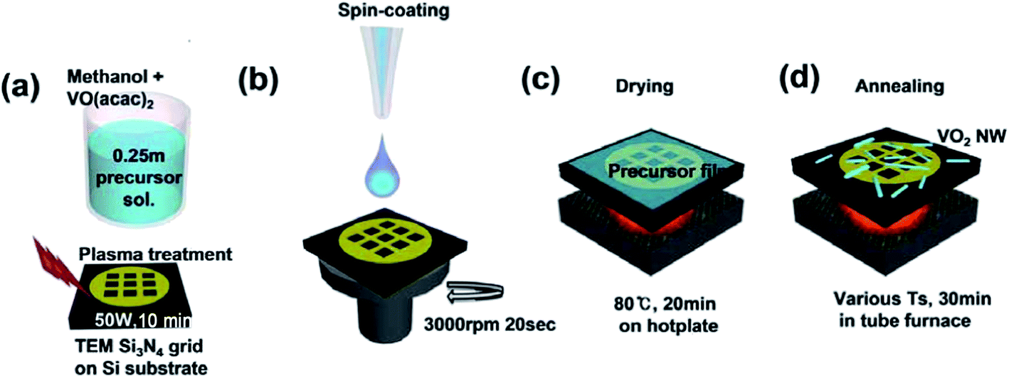 | ||
| Fig. 1 Schematic describing the synthetic procedure to fabricate VO2 nanostructures on a customized Si3N4 TEM grid. | ||
2.2. Structural, morphological, and chemical characterizations
The evolution of the nanostructure morphology was examined by a field-emission TEM (Tecnai G2 F30 S-Twin, 300 KeV, FEI). Additionally, the compositions of the structures were measured using a scanning transmission electron microscope (STEM) and an energy-dispersive X-ray spectroscope (EDS) that were installed in the TEM. To confirm the composition, auger electron spectroscopy (AES) was utilized. The crystalline structure of the individual VO2 nanowires was investigated using a high-resolution Raman spectroscope in a back scattering geometry using a laser operating at 488 nm excitation with a spatial resolution of 500 nm and spectral resolution of 0.7 cm−1. A laser power of approximately 30 μW was used to avoid heating effects of the samples under the focused laser beam. The incident light was polarized along the parallel length of the wire (CR) to yield a superposition the Ag and Bg mode in the interaction between the polarized and un-polarized signal. In addition, X-ray diffraction studies were performed using a Rigaku D/max-2500 diffractometer with Cu-Kα radiation (λ = 1.54 Å) at 40 kV and 100 mA.2.3. Electrical characterization
To directly compare the electronic MIT properties of the individual VO2 nanowires with their structural characteristics, which can only be examined using TEM due to the small diameters of the wires, we exploited the focused ion beam (FIB) technique to deposit metal (Pt) electrodes to fabricate individual nanowire devices directly on the customized grids. The electrical properties of the individual nanowire devices were measured by a semiconductor characterization system (Keithley 4200 SCS) on a temperature-controlled heating stage, whose resolution was within 0.1 °C (Linkam LTS420). Note that we performed the measurements with an upper current compliance of 200 μA to limit the Joule heating caused by excessive current.3. Results and discussion
3.1. Effects of temperature on morphological transition of VO2 nanostructures
The morphological change and development of the VO2 nanostructures spin-coated from the sol–gel solution during annealing under Ar gas flow were investigated using several TEM techniques, including bright-field (BF) imaging, selected-area electron diffraction (SAED), high-resolution TEM (HRTEM) imaging, and fast Fourier transformation (FFT). Fig. 2(a–t) show the measured images and patterns of the sample after annealing at various temperatures (80, 300, 400, 450, 500, and 550 °C) for 30 minutes. At each temperature, we assembled a set of BF and HRTEM images with their corresponding SAED and FFT patterns.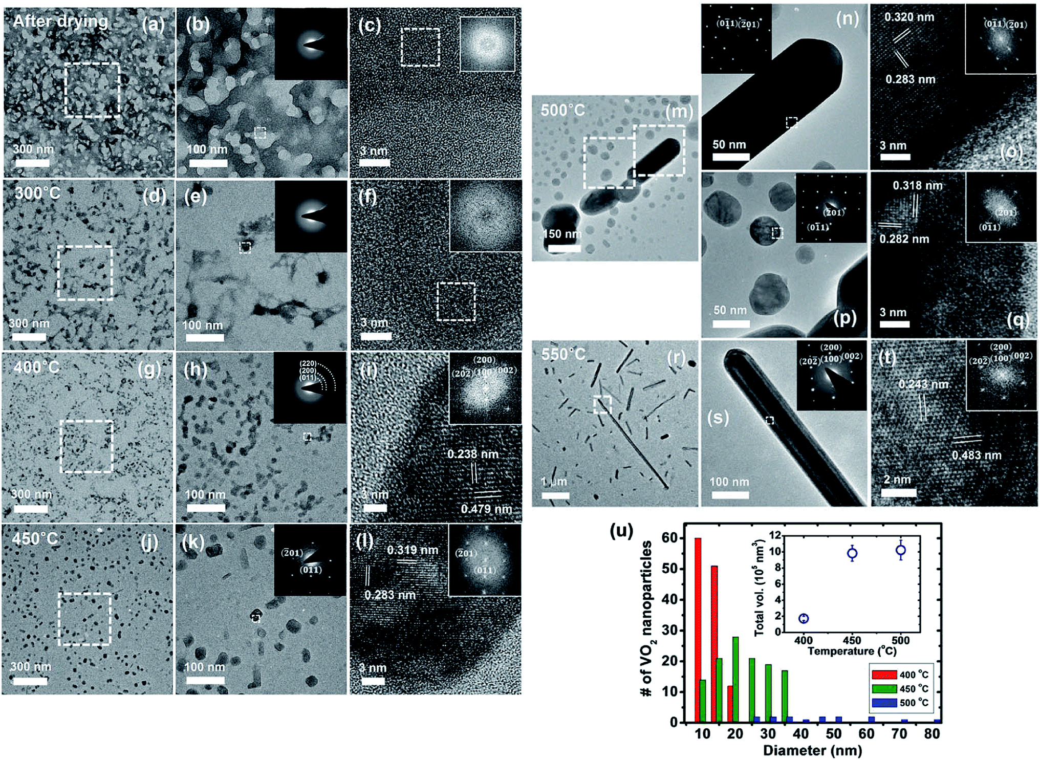 | ||
| Fig. 2 TEM images of the spin-coated sol–gel film during annealing and analysis of the particle distribution. (a and b) BF images of a broad view of the sample annealed at 80 °C for 30 minutes and a magnified view of the dotted box in (a). (Inset of (b)) The selected-area electron diffraction (SAED) pattern of the sample. (c) The high-resolution TEM (HRTEM) image of the box in (b). (Inset of (c)) The fast Fourier transformation (FFT) of the dotted box in (c). This sequence of images and patterns are repeated for the samples annealed at temperatures of (d–f) 300 °C, (g–i) 400 °C, (j–l) 450 °C, (m–q) 500 °C, and (r–t) 550 °C with identical annealing durations. An exception exists for (m–q): (m–o) the initial growth of the nanowire and (m, p and q) the coarsened nanoparticle. (u) Number of particles versus diameter at 400, 450, and 500 °C. | ||
Fig. 2a and b present broad and magnified views of the coated film after annealing at 80 °C. The brighter and darker contrasts represent the Si3N4 membrane and the film, respectively. The HRTEM image and the FFT pattern in Fig. 2c, obtained from a portion of the film (the dotted box), demonstrate that the film consists of an amorphous phase and provides evidence that organic components were present after evaporation of the solvent (methanol), which has a boiling point of 64.7 °C. The organic precursors agglomerated at 300 °C, as identified in the HRTEM image of the amorphous pattern taken from the area of the dotted box in Fig. 2f. Annealing at 400 °C accelerated the removal of the organics and promoted the evolution of a few VO2 nanoparticles, as shown in Fig. 2g–i. In detail, the SAED pattern in the inset of Fig. 2h reveals polycrystalline rings that correspond to the (011), (200) and (220) lattice planes, which are in agreement with the JCPDS34 data for monoclinic-phase VO2 (M1) (see the magnified index pattern in ESI Fig. S1†). This is confirmed by the HRTEM image in Fig. 2i taken at [010], which provided lattice spacings of 0.479 nm and 0.227 nm for the (100) and (002) planes, respectively.
The BF image in Fig. 2j exhibits the complete removal of organic components and the spatial distributions of the VO2 nanoparticles in the M1 phase after annealing at 450 °C. The diameters of the particles are in a range of 12.5–35.0 nm (see Fig. 2u). Again, the crystalline structure of the VO2 particles is monoclinic (M1), given that the measured values of the lattice spacings of the (0![[1 with combining macron]](https://www.rsc.org/images/entities/char_0031_0304.gif) 1) and (
1) and (![[2 with combining macron]](https://www.rsc.org/images/entities/char_0032_0304.gif) 01) planes from the HRTEM image and the FFT pattern taken at [122] in Fig. 2l are 0.319 nm and 0.283 nm, respectively. At 500 °C, the BF image in Fig. 2m shows an increased size distribution of the particles, ranging from 24.7 to 83.5 nm, compared to that at 450 °C (see the data for the number of particles versus the diameter in Fig. 2u). This phenomenon can be attributed to the coarsening of the particles during annealing. Additionally, the inset of Fig. 2u presents the temperature dependence of the total volume of the particles, indicating that no additional conversion from the organic precursor to the crystalline particle occurs over 450 °C. We also observed the initial moment when the particles transformed into nanowires through the preferential attachment of diffused atoms to the [100] growth direction, in comparison with the sidewall [01] direction, as presented in the BF image and the SAED pattern (see Fig. 2n). Both the particles and wires were found to be in the M1 phase, as shown in the SAED and FFT patterns in Fig. 2n and o. When the temperature was increased to 550 °C, most of the nanoparticles were converted to nanowires, and the length of the wire became much longer than those at 500 °C, as exhibited in Fig. 2r. The SAED pattern and the HRTEM image taken along the [010] direction of an individual nanowire indicate that it is single crystalline with interplanar spacings of 0.483 nm and 0.226 nm for the (100) and (002) planes, respectively.33 Consequently, the annealing data provide evidence that the annealing temperature is a crucial parameter to control the morphology of VO2 nanostructures.
01) planes from the HRTEM image and the FFT pattern taken at [122] in Fig. 2l are 0.319 nm and 0.283 nm, respectively. At 500 °C, the BF image in Fig. 2m shows an increased size distribution of the particles, ranging from 24.7 to 83.5 nm, compared to that at 450 °C (see the data for the number of particles versus the diameter in Fig. 2u). This phenomenon can be attributed to the coarsening of the particles during annealing. Additionally, the inset of Fig. 2u presents the temperature dependence of the total volume of the particles, indicating that no additional conversion from the organic precursor to the crystalline particle occurs over 450 °C. We also observed the initial moment when the particles transformed into nanowires through the preferential attachment of diffused atoms to the [100] growth direction, in comparison with the sidewall [01] direction, as presented in the BF image and the SAED pattern (see Fig. 2n). Both the particles and wires were found to be in the M1 phase, as shown in the SAED and FFT patterns in Fig. 2n and o. When the temperature was increased to 550 °C, most of the nanoparticles were converted to nanowires, and the length of the wire became much longer than those at 500 °C, as exhibited in Fig. 2r. The SAED pattern and the HRTEM image taken along the [010] direction of an individual nanowire indicate that it is single crystalline with interplanar spacings of 0.483 nm and 0.226 nm for the (100) and (002) planes, respectively.33 Consequently, the annealing data provide evidence that the annealing temperature is a crucial parameter to control the morphology of VO2 nanostructures.
3.2. Effects of temperature on compositional transition of VO2 nanostructures
To clearly correlate the surface morphology and crystalline structure with the composition of the sol–gel film, we performed STEM and EDS analyses of the sample at room temperature after annealing at different temperatures. Fig. 3a–f display a series of high-angle annular dark field (HAADF) STEM images, which correspond to the morphological transition obtained from the TEM measurements discussed in Fig. 2. Using the spot EDS measurement based on the STEM images, we determined the V/O compositional ratios with respect to the annealing temperature, as well as the three regimes classified by the morphology of the film (see Fig. 3g). For the samples annealed at each temperature, we selected more than 10 different locations to acquire the average composition (see the representative EDS data in ESI Fig. S2†). In regime I (below 80 °C), where only the solvent was evaporated, the V/O ratio was nearly 0.2, which is consistent with the V/O molar ratio of the precursor (VO(acac)2, C10H14O5V) used for spin-coating. In regime II, we discovered that the V/O ratio of the coated film increased from 0.2 to 0.5 as the temperature increased, implying that oxygen reduction progressed until the film transformed to VO2, as the valence of vanadium in VO(acac)2 is four.34 Finally, in regime III (over 400 °C), the stoichiometry for VO2 remained constant during the morphological transition, as droplet coarsening was active.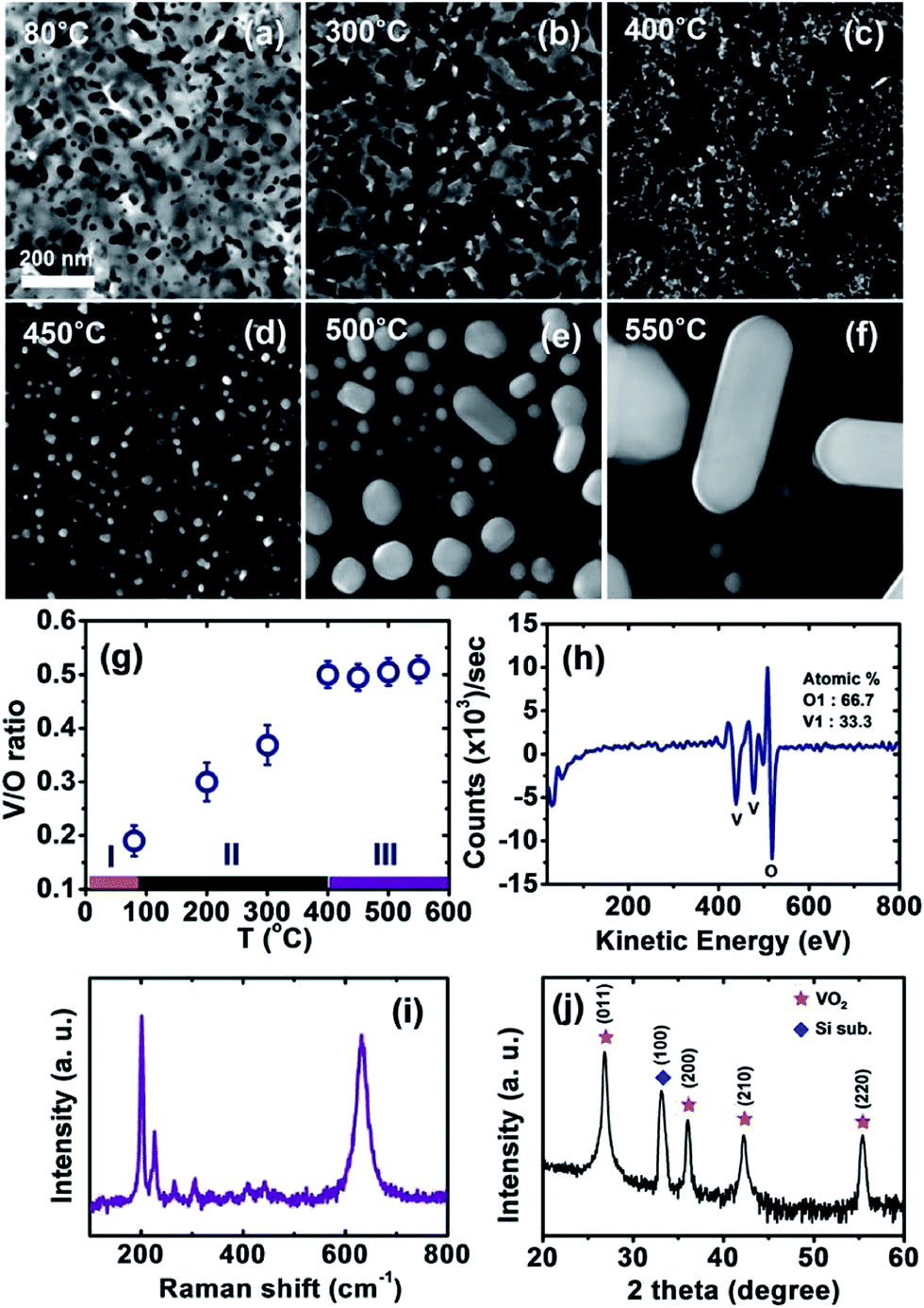 | ||
| Fig. 3 STEM and EDS analyses of the spin-coated sol–gel film and other characterizations to identify the crystalline structure of the VO2 nanowire. (a–f) A series of HAADF STEM images of the sequential morphological transitions obtained from the TEM measurements shown in Fig. 2. (g) Spot EDS measurements to obtain the V/O compositional ratios with respect to the annealing temperature in comparison with the three regimes classified by the film morphology. (h–j) AES spectroscopy, Raman spectroscopy, and XRD measurements of the nanowire annealed at 550 °C, respectively. | ||
We confirmed using AES spectroscopy that the composition of the nanowires after annealing at 550 °C was V:O = 1:2, as exhibited in Fig. 3h. Moreover, the crystalline structure of the VO2 nanowires was characterized by Raman spectroscopy (see Fig. 3i), which showed the typical features of the M1 phase. This was also verified by high-resolution XRD (where λ = 1.541 Å), which showed the indexed diffraction peaks of the M1 phase (i.e., (011), (200), (210), and (220))34 and the silicon substrate, as shown in Fig. 3j.
3.3. In situ Raman and TEM analyses of metal–insulator transition (MIT) in VO2 nanowires
To directly compare the phase transition behaviors of individual VO2 nanowires, we first formed VO2 nanowires on the Si3N4 membrane of a TEM grid through annealing, as mentioned above. Fig. 4a presents the Raman spectra acquired from an individual VO2 nanowire as a function of temperature across the metal–insulator transition. The Raman spectroscopy data show the characteristic features of the M1 phase up to 69 ± 0.1 °C. Thereafter, VO2 was quickly transformed into the metallic R phase, as evidenced by an abrupt loss of all Raman-active modes. Then, the sample cooled, the M1 phase was recovered at 64 ± 0.1 °C, displaying a temperature hysteresis. The hysteresis may be related to the nucleation energy barrier to transform to the M1 phase from the R phase and possibly to the friction between the wire and the substrate. In contrast to the VO2 nanowires grown on crystalline substrates via the vapor transport method, which accumulates tensile stress from the lattice mismatch with the substrate,35 our nanowires, fabricated by a solution process, did not enter the M2 phase (which is normally determined by a shift of the peak at 607 cm−1 to 649 cm−1) during the phase transition. | ||
| Fig. 4 In situ TEM and Raman spectroscopy examinations. (a) In situ Raman spectra acquired from an electrode-free VO2 nanowire as a function of temperature across the metal–insulator transition. (b) A sequence of in situ TEM DF images of the electrode-free VO2 nanowire during temperature cycling: the brighter area is the M1 phase, while the darker area is the R phase. The scale bar is 1 μm. (c) In situ Raman spectra acquired from an electrode-clamped VO2 nanowire as a function of temperature across the metal–insulator transition. (d) A sequence of in situ TEM DF images of the electrode-clamped VO2 nanowire during temperature cycling: the brighter area is the M1 phase, while the darker area is the R phase. The scale bar is 1 μm. (e) The SAED pattern of the nanowire. | ||
A temperature cycling experiment of an individual nanowire was conducted by TEM DF imaging to quantitatively identify the proportion of each phase during the metal–insulator transition. Fig. 4b shows a sequence of DF images taken using the () diffracted spot close to the [01] zone axis in the monoclinic structure (M1) with respect to the temperature (see the SAED pattern of the wire in Fig. 4e). At room temperature, the whole wire was in the M1 phase, as reflected by the bright contrast in the wire. As the temperature increased, the nanowire remained in the M1 phase until it suddenly transformed to the R phase, as shown by the completely dark contrast, at 69 °C over a span of ∼0.1 °C. We increased temperature by 0.1 °C at each step for accurate measurements of the transition temperatures. After each step of temperature increase, we confirmed the identity of the phase by using the SAED with a small aperture (250 nm in diameter), as we moved the aperture with a distance of 50 nm over the entire wire, and the HRTEM. This ensures the reliability of identifying the phase of the domain.
Considering such transition properties of the nanowires, obtained from the two in situ instruments under the synthetic conditions, we assume that the nanowire is stress-free with high single crystallinity and excellent stoichiometric homogeneity across the wire. This postulation may be reasonable because the adhesion at the interface between the nanowire and the substrate is not strong enough to prevent the wire from sliding on the substrate during the transition. Otherwise, the wire would have transformed over a much wider temperature range and may create M2 phase due to the tensile stress from the interface.36 We believe that this situation can be ascribed to the relatively low annealing temperature used to create the nanowires. After this event, lowering the temperature drove the wire to quickly recover the M1 phase at nearly 64 °C over a span of ∼0.1 °C.
To further understand the phase transition behavior of the nanowire examined above, we fabricated a two-terminal individual-wire device. The overview of the device was taken by SEM as shown in ESI Fig. S3.† FIB allowed us to deposit Pt electrodes on both ends of the wire with a channel length of ∼6 μm. Similar to the measurement of the electrode-free wire, we first investigated the wire using Raman spectroscopy during temperature cycling, as shown in Fig. 4c. As the temperature increased, the wire remained in the M1 phase up to 74.7 °C, which is significantly higher than that of the electrode-free wire, followed by a transition to the R phase at 75.5 °C. Then, the wire returned to the M1 phase at 66.0 °C.
The results of the corresponding in situ TEM DF imaging measurements of the temperature dependence of the phase transition of the nanowire in the device, as shown in Fig. 4d, were mostly consistent with the Raman spectroscopy results, with approximately the same transition temperature. However, we identified that the transition from the M1 phase to the R phase included a mixed phase regime from 74.7 to 75.4 °C, where the M1 and R phases coexist. This phenomenon could not be detected by Raman spectroscopy due to its spatial resolution limit. Interestingly, this regime began with the multiple nucleation of the R phase from the M1 phase, as shown by the dark contrasted segments spread on the bright background in the DF image taken at 74.9 °C, forming a roughly periodic domain distribution across the wire. This can be explained by the reasonable assumption that the wire was subjected to tensile stress resulting from the champed electrode when the temperature was higher than the transition temperature (∼69 °C) of the electrode-free wire. Generally, a nanowire can relax stored stress by forming multiple R phase domains, which creates an increased total interfacial area between the M1 and R phases in the wire.36 Upon cooling, the M1 phase was suddenly restored at approximately 66.0 °C, similar to the result obtained by Raman spectroscopy. We note that the other TEM analyses using BF, SAED patterns, HRTEM imaging, and FFT patterns of the VO2 nanowire in the device confirm the phase transition as shown in ESI Fig. S4.†
Fig. 5a presents the temperature dependence of the resistance (R) for the individual nanowire device discussed in Fig. 4c and d. The varying resistance during the heating and cooling cycle corresponds to the common behavior of VO2, which exhibits a slow decrease in the insulating state of the monoclinic phase M1 followed by an abrupt decrease in the metallic state of the rutile phase; when the temperature is reversed, hysteresis occurs. This is a pronounced switching characteristic of stoichiometric VO2via its first-order transition.9,10 The R vs. T curve during heating illustrates that the transition from the insulating to the metallic phase is characterized by a nearly three orders of magnitude decrease in the resistance within a span of 0.7 °C (beginning at 74.5 °C and ending at 75.2 °C). The transition back to the insulating phase is similarly abrupt, occurring across a span of ∼0.2 °C (beginning at 66.2 °C and ending at 66 °C) with a hysteresis of approximately 8.7 °C. We note that of the 8 individual nanowire devices tested, the insulator-to-metal transition occurred at a temperature of 75 ± 2 °C, with the transition occurring within 1 °C.
 | ||
| Fig. 5 Electrical transport properties of the individual nanowire device. (a) The temperature dependence of the resistance (R) for the individual-nanowire device discussed in Fig. 4c and d. (b) The temperature-dependent current–voltage measurements of the same device and (c) a plot of Vthvs. Vth ∝ (Tc − T)1/2 to clarify the mechanism of the IMT phenomenon. | ||
Normally, during heating, the nanowire shows a slight discontinuous jump in resistance in the insulating state, indicating that the M1 phase in the wire transforms into the M2 phase, which typically occurs prior to the transformation to the metallic R phase, typically owing to the internal stress in the wire occurring during growth and/or the external stress from electrodes during the phase transition.35 However, the nanowire prepared by sol–gel spin-coating does not exhibit this jump, although the electrodes at both ends of the wire provide tensile stress during the transition. From this, we could postulate that the high crystallinity of the wire limits the number of possible nucleation sites and thereby can kinetically prevent the wire from transforming to the M2 phase, allowing it to directly convert to the R phase with a larger hysteresis than observed in the Raman data of the electrode-free wire.37 Therefore, we can assume that at temperatures up to 69 °C, at which the electrode-free wire began to transform from the M1 phase to the R phase, the wire in a device would not be subjected to any stress from the electrodes. This can be simply confirmed by fitting the data of the M1 phase up to 69 °C, which presents Arrhenius behavior, with R(T) = R0exp(Eg/2kT), where k is Boltzmann's constant and T is the temperature, as shown in the inset of Fig. 5a. This yielded a thermal activation energy of 0.295 ± 0.05 eV, which is consistent with the optical band gap energy of 0.60 eV of a stress-free single-crystalline VO2 nanowire.38
Fig. 5b exhibits the temperature-dependent current–voltage measurements of the same device as in Fig. 4c and d and 5a. For temperatures below Tc, the current increases slowly as the voltage increases, and upon reaching a specific threshold voltage (Vth), a discontinuous increase in the current is evidenced, indicating an insulator-to-metal transition (IMT). Above Vth, the I–V curves become flat as the current reaches the compliance limit. It is clearly observed that the Vth for the IMT decreases with increasing temperature. In the transition from the insulating phase to the metallic phase, the threshold voltage for the transition shows an approximately Vth ∝ (Tc − T)1/2 dependence (see Fig. 5c), revealing that the Joule heating that leads to a local temperature increase may be the primary mechanism driving the IMT in the VO2 nanowire device.39,40
4. Conclusion
In conclusion, we demonstrated the morphological transition of VO2 nanostructures in a sol–gel film spin-coated on a customized TEM grid, as well as illustrated the reaction mechanism driven by oxygen reduction during annealing. In situ TEM DF imaging and Raman spectroscopy allowed us to verify the outstanding phase transition properties of individual nanowires and examined the effect of the tensile stress from electrode-clamping on the formation of R phase domains. Furthermore, we measured the resistance of the electrode-clamped wire as a function of temperature and found that the approximately 600 mV electrical band gap of the wire, which is close to the optical band gap of VO2, can be attributed to the superior control of the stoichiometry and crystallinity of the wire. We also identified that the temperature dependence of the threshold voltage (Vth) can be associated with the Joule heating. The data shown here provide us with important information for controlling the morphology, size, dimensions, uniformity, crystallinity and stoichiometry of VO2 nanostructures synthesized by the sol–gel method, as well as suggest a novel route to fabricate VO2 nanowires with clear MIT properties. Moreover, a direct comparison between the structural, chemical and electrical aspects of individual nanowires would significantly enhance the advancements of VO2 applications.Conflicts of interest
The authors declare no competing financial interest.Acknowledgements
This work was supported by the Samsung Research Funding Center of Samsung Electronics under Project Number SRFC-MA1402-10.References
- Z. Yang, C. Ko and S. Ramanathan, Oxide Electronics Utilizing Ultrafast Metal-Insulator Transitions, Annu. Rev. Mater. Res., 2011, 41, 337 CrossRef.
- D. Ruzmetov, G. Gopalakrishnan, C. Ko, V. Narayanamurti and S. Ramanathan, Three-Terminal Field Effect Devices Utilizing Thin Film Vanadium Oxide as the Channel Layer, J. Appl. Phys., 2010, 107, 114516 CrossRef.
- S. Y. Li, K. Namura, M. Suzuki, G. A. Niklasson and C. G. Granqvist, Thermochromic VO2 Nanorods Made by Sputter Deposition: Growth Conditions and Optical Modeling, J. Appl. Phys., 2013, 114, 033516 CrossRef.
- A. Gentle, A. I. Maaroof and G. B. Smith, Nanograin VO2 in the metal phase: a plasmonic system with falling dc resistivity as temperature rises, Nanotechnology, 2007, 18, 025202 CrossRef.
- J. I. Sohn, H. J. Joo, A. E. Porter, C. J. Choi, K. Kim, D. J. Kang and M. E. Welland, Direct Observation of the Structural Component of the Metal–Insulator Phase Transition and Growth Habits of Epitaxially Grown VO2 Nanowires, Nano Lett., 2007, 7, 1570 CrossRef PubMed.
- M. J. Lee, Y. Park, D. S. Suh, E. H. Lee, S. Seo, D. C. Kim, R. Jung, B. S. Kang, S. E. Ahn, C. B. Lee, D. H. Seo, Y. K. Cha, I. K. Yoo, J. S. Kim and B. H. Park, Two Series Oxide Resistors Applicable to High Speed and High Density Nonvolatile Memory, Adv. Mater., 2007, 19, 3919 CrossRef.
- M. Gurvitch, S. Luryi, A. Polyakov, A. Shabalov, M. Dudley, G. Wang, S. Ge and V. Yakovlev, VO2 films with strong semiconductor to metal phase transition prepared by the precursor oxidation process, J. Appl. Phys., 2007, 102, 033504 CrossRef.
- G. Armstrong, J. Canales, A. R. Armstrong and P. G. Bruce, The synthesis and lithium intercalation electrochemistry of VO2(B) ultra-thin nanowires, J. Power Sources, 2008, 178, 723 CrossRef.
- F. J. Morin, Oxides Which Show a Metal-to-Insulator Transition at the Neel Temperature, Phys. Rev. Lett., 1959, 3, 34 CrossRef.
- J. I. Sohn, H. J. Joo, K. S. Kim, H. W. Yang, A. R. Jang, D. C. Ahn, H. H. Lee, S. N. Cha, D. J. Kang and J. M. Kim, Stress-induced domain dynamics and phase transitions in epitaxially grown VO2 nanowires, Nanotechnology, 2012, 23, 205707 CrossRef PubMed.
- M. M. Qazilbash, M. Brehm, B. G. Chae, P. C. Hol, G. O. Andreev, B. J. Kim, S. J. Yun, A. V. Baltatsky, M. B. Maple, F. Keilmann, H. T. Kim and D. N. Basov, Mott transition in VO2 revealed by infrared spectroscopy and nano-imaging, Science, 2007, 318, 1750 CrossRef PubMed.
- M. M. Qazilbash, K. S. Burch, D. Whisler, D. Shrekenhamer, B. G. Chae, H. T. Kim and D. N. Basov, Correlated metallic state of vanadium dioxide, Phys. Rev. B, 2006, 74, 205118 CrossRef.
- A. Cavalleri, M. Rini, H. H. W. Chong, S. Fourmaux, T. E. Glover, P. A. Heimann, J. C. Kieffer and R. W. Schoenlein, Band-selective measurements of electron dynamics in VO2 using femtosecond near-edge X-ray absorption, Phys. Rev. Lett., 2005, 95, 067405 CrossRef PubMed.
- S. Biermann, A. Poteryaev, A. I. Lichtenstein and A. Georges, Dynamical singlets and correlation-assisted Peierls transition in VO2, Phys. Rev. Lett., 2005, 94, 026404 CrossRef PubMed.
- M. M. Qazilbash, A. Tripathi, A. A. Schafgans, B. J. Kim, H. T. Kim, Z. Cai, M. V. Holt, J. M. Maser, F. Keilmann, O. G. Shpyrko and D. N. Basov, Nanoscale imaging of the electronic and structural transitions in vanadium dioxide, Phys. Rev. B, 2011, 83, 165108 CrossRef.
- S. Zhang, I. S. Kim and L. J. Lauhon, Stoichiometry engineering of monoclinic to rutile phase transition in suspended single crystalline vanadium dioxide nanobeams, Nano Lett., 2011, 11, 1443–1447 CrossRef PubMed.
- C. Ko, Z. Yang and S. Ramanathan, Work function of vanadium dioxide thin films across the metal–insulator transition and the role of surface nonstoichiometry, ACS Appl. Mater. Interfaces, 2011, 3, 3396–3401 CrossRef PubMed.
- Z. Zhang, Y. Gao, L. Kang, J. Du and H. Luo, Effects of a TiO2 buffer layer on solution-deposited VO2 films: enhanced oxidization durability, J. Phys. Chem. C, 2010, 114, 22214–22220 CrossRef.
- J. Zhou, Z. Zhou, Y. Gao, X. Liu, Z. Chen, L. Dai, C. Cao, H. Luo, M. Kanahira, C. Sun and L. Yan, Mg-doped VO2 nanoparticles: hydrothermal synthesis, enhanced visible transmittance and decreased metal–insulator transition temperature, Phys. Chem. Chem. Phys., 2013, 15, 7505–7511 RSC.
- L. Dai, S. Chen, J. Liu, Y. Gao, J. Zhou, Z. Chen, C. Cao, H. Luo and M. Kanehira, F-doped VO2 nanoparticles for thermochromic energy-saving foils with modified color and enhanced solar-heat shielding ability, Phys. Chem. Chem. Phys., 2013, 15, 11723 RSC.
- Y. Gao, C. Cao, L. Dai, H. Luo, M. Kanehira, Y. Ding and Z. L. Wang, Phase and shape controlled VO2 nanostructures by antimony doping, Energy Environ. Sci., 2012, 5, 8708 RSC.
- L. Dai, C. Cao, Y. Gao and H. Luo, Synthesis and phase transition behavior of undoped VO2 with a strong nano-size effect, Sol. Energy Mater. Sol. Cells, 2011, 95, 712 CrossRef.
- J. Cao, E. Ertekin, V. Srinivasan, W. Fan, S. Huang, H. Zheng, J. W. L. Yim, D. R. Khanal, D. F. Ogletree, J. C. Grossman and J. Wu, Strain engineering and one-dimensional organization of metal–insulator domains in single-crystal vanadium dioxide beams, Nat. Nanotechnol., 2009, 4, 732 CrossRef PubMed.
- J. M. Atkin, S. Berweger, E. K. Chavez, M. B. Raschke, J. Cao, W. Fan and J. Wu, Strain and temperature dependence of the insulating phases of VO2 near the metal–insulator transition, Phys. Rev. B, 2012, 85, 020101 CrossRef.
- J. Wu, Q. Gu, B. S. Guiton, N. P. D. Leon, L. Ouyang and H. K. Park, Strain-Induced Self Organization of Metal–Insulator Domains in Single-Crystalline VO2 Nanobeams, Nano Lett., 2006, 6, 2313 CrossRef PubMed.
- Y. Cheng, T. Zhang, Y. Cai, K. M. Ho, K. K. Fung and N. Wang, Structure and metal-to-insulator transition of VO2 nanowires grown on sapphire substrates, Eur. J. Inorg. Chem., 2010, 4332 CrossRef.
- B. S. Guiton, Q. Gu, A. L. Prieto, M. S. Gudiksen and H. Park, Single-Crystalline Vanadium Dioxide Nanowires with Rectangular Cross Sections, J. Am. Chem. Soc., 2005, 127, 498 CrossRef PubMed.
- L. Q. Mai, B. Hu, T. Hu, W. Chen and E. D. J. Gu, Electrical Property of Mo-Doped VO2 Nanowire Array Film by Melting-Quenching Sol–Gel Method, J. Phys. Chem. B, 2006, 110, 19083 CrossRef PubMed.
- E. Baudrin, G. Sudant, D. Larcher and B. Dunn, Tarascon, Preparation of Nanotextured VO2[B] from Vanadium Oxide Aerogels, J. Mater. Chem., 2006, 18, 4369 CrossRef.
- R. Binions, G. Hyett, C. Piccirillo and I. P. Parkin, Doped and un-doped vanadium dioxide thin films prepared by atmospheric pressure chemical vapour deposition from vanadyl acetylacetonate and tungsten hexachloride: the effects of thickness and crystallographic orientation on thermochromic properties, J. Mater. Chem., 2007, 17, 4652 RSC.
- R. Lopez, R. F. Haglund and L. C. Feldman, Two-dimensional current percolation in nanocrystalline vanadiumdioxide films, Appl. Phys. Lett., 2006, 88, 081902 CrossRef.
- Y. T. Wang and C. H. Chen, Facile Growth of Thermochromic VO2 Nanostructures with Greatly Varied Phases and Morphologies, Inorg. Chem., 2013, 52, 2550 CrossRef PubMed.
- JCPDS of monoclinic-phase (M1) VO2: No. 72-0514.
- M. Pan, H. Zhong, S. Wang, J. Liu, Z. Li, X. Chen and W. Lu, Properties of VO2 thin film prepared with precursor VO(acac)2, J. Cryst. Growth, 2004, 265, 121 CrossRef.
- M. W. Kim, S. S. Ha, O. K. Seo, D. Y. Noh and B. J. Kim, Real-Time Structural and Electrical Characterization of Metal–Insulator Transition in Strain-Modulated Single-Phase VO2 Wires with Controlled Diameters, Nano Lett., 2016, 16, 4074 CrossRef PubMed.
- J. Wu, Q. Gu, B. S. Guiton, N. P. D. Leon, L. Ouyang and H. K. Park, Strain-Induced Self Organization of Metal–Insulator Domains in Single-Crystalline VO2 Nanobeams, Nano Lett., 2006, 6, 2313 CrossRef PubMed.
- G. A. Horrocks, S. Singh, M. F. Likely, G. Sambandamurthy and S. Banerjee, Scalable Hydrothermal Synthesis of Free-Standing VO2 Nanowires in the M1 Phase, ACS Appl. Mater. Interfaces, 2014, 6, 15726 CrossRef PubMed.
- Z. Wei, Z. Wang, W. Chen and D. H. Cobden, New aspects of the metal–insulator transition in single-domain vanadium dioxide nanobeams, Nat. Nanotechnol., 2009, 4, 420 CrossRef PubMed.
- Y. R. Jo, M. W. Kim and B. J. Kim, Direct correlation of structural and electrical properties of electron-doped individual VO2 nanowires on devised TEM grids, Nanotechnology, 2016, 27, 435704 CrossRef PubMed.
- M. W. Kim, W. G. Jung, H. Cho, T. S. Bae, S. J. Chang, J. S. Jang, W. K. Hong and B. J. Kim, Substrate-mediated strain effect on the role of thermal heating and electric field on metal–insulator transition in vanadium dioxide nanobeams, Sci. Rep., 2015, 5, 10861 CrossRef PubMed.
- C. Cheng, K. Liu, B. Xiang, J. Suh and J. Wu, Ultra-long, free-standing, single-crystalline vanadium dioxide micro/nanowires grown by simple thermal evaporation, Appl. Phys. Lett., 2012, 100, 103111 CrossRef.
- S.-H. Bae, S. Lee, H. Koo, L. Lin, B. H. Jo, C. Park and Z. L. Wang, The Memristive properties of a single VO2 nanowire with switching controlled by self-heating, Adv. Mater., 2013, 25, 5098 CrossRef PubMed.
- H. Zhang, Q. Li, P. Shen, Q. Dong, B. Liu, R. Liu, T. Cui and B. Liu, The structural phase transition process of freestanding monoclinic vanadium dioxide micronsized rods: temperature-dependent Raman study, RSC Adv., 2015, 5, 83139 RSC.
Footnote |
| † Electronic supplementary information (ESI) available. See DOI: 10.1039/c7ra10865f |
| This journal is © The Royal Society of Chemistry 2018 |