
 Open Access Article
 This Open Access Article is licensed under a Creative Commons Attribution-Non Commercial 3.0 Unported Licence
Oxygen vacancy and doping atom effect on electronic structure and optical properties of Cd2SnO4
Mei Tang ab,
JiaXiang Shanga and
Yue Zhang*a
ab,
JiaXiang Shanga and
Yue Zhang*a
aSchool of Materials Science and Engineering, Beihang University, Beijing 100191, China. E-mail: zhangy@buaa.edu.cn
bJournal Publishing Center of Tsinghua University Press, Beijing 100084, China
First published on 2nd January 2018
Abstract
The electronic structure and optical properties of oxygen vacancy and La-doped Cd2SnO4 were calculated using the plane-wave-based pseudopotential method based on the density functional theory (DFT) within the generalized gradient approximation (GGA). The formation energy of different oxygen vacancies showed that the VO2 oxygen vacancy was easy to obtain in experiments. The Bader charge analysis is implemented to directly observe the electron transfer and distribution for each atom. The calculated band structures show that when the oxygen vacancy was introduced, the impurity energy level appeared in the band gap. The impurity levels induced by oxygen vacancies were mainly composed of O 2p orbits and a very small amount of Cd 4s orbits. After La doping based on the VO2 oxygen vacancy of Cd2SnO4, the Fermi energy level entered the conduction band and overlapped with the conduction band which increased the conductivity, and the band gap value increased to above 3.0 eV. The optical calculation results showed that the transmittance of the VO2 oxygen vacancy of Cd2SnO4 increased in short wavelength (<600 nm), the reflectivity increased in the infrared region compared with Cd2SnO4, and the transmittance increased to 90% in visible light region after La doping.
I. Introduction
Cadmium stannate (CTO), first discovered in 1960 by Smith, is an important transparent conductive material with great potential to be applied in thin film solar cells and other devices that require low resistance transparent conductive films.1–3 After grinding cadmium carbonate and tin oxide powder, the powder was sintered at high temperature, and the obtained cadmium stannate powder was determined by X-ray diffraction measurement. The Cd2SnO4 was light yellow and had an orthorhombic crystal structure, and the crystal lattice constant was also listed by Smith.4 Since then, researchers in the 1960s studied Cd2SnO4, and Smith's work was repeated. In 1972, a Cd2SnO4 film was prepared by radioactive magnetron sputtering of a cadmium stannate ceramic target for the first time by Nozik.5 The sputtering atmosphere was mixed with argon and argon–oxygen atmosphere, and the film was annealed at low temperature for a long time. The optical bandgap and mobility of the film were measured to obtain a conductivity of 1.33 × 10³ Ω−1 cm−1. In 2000, after the use of CTO films for CdTe solar cells, Cd2SnO4 was gaining wide attention.6 In 2001, Wu used CTO thin film as the transparent electrode of CdTe solar cells, and obtained 16.5% solar cell photoelectric conversion efficiency, the world's highest from CdTe.7A variety of methods for preparing the Cd2SnO4 film were then attempted, including chemical vapor deposition (CVD) method,8 pulsed laser deposition (PLD) method,9 spray pyrolysis method,10 sol–gel method,11,12 electron beam evaporation method,13 DC sputtering14–17 and RF sputtering.18–21 In many of the preparation methods, the CTO films prepared by magnetron sputtering had the lowest resistivity, and the resistivity of films prepared by various magnetron sputtering methods was much lower compared with other methods. In all experiments using magnetron sputtering to deposit CTO thin films, we found that most of the deposited films were heat treated,22–24 and when the deposition atmosphere contained oxygen, the CTO film can be a low resistance film after heat treatment. The resistivity of the film deposited in the oxygen-containing atmosphere was higher, and the resistivity of the film after annealing in rare gas and reducing hydrogen was lower, and the resistivity of the film was higher after annealing in an oxygen-containing atmosphere. The resistivity of the films deposited in the argon atmosphere was low, but the resistivity results of different films obtained by different researchers after annealing in different atmospheres were different.
However, there were only a few detailed studies of the conductive mechanism of oxygen vacancy of the CTO thin films in the literature.25 For example, Stapiński et al.26 prepared Cd2SnO4 thin films by DC reactive sputtering, analyzed the types of carriers in the films, it is considered that the carriers in the Cd2SnO4 film was oxygen vacancy or cadmium gap atom. But, oxygen vacancies or cadmium gap atoms provided more carriers that had not been studied. It had been suggested that cadmium atoms were occupied by tin atoms, which were also sources of carriers.27 Ion doping is a method to improve the optical absorption characteristics of materials by introducing different impurity ions, controlling the micro crystal structure and changing the band structure. The rare earth elements possess many special photoelectric properties because of their incomplete occupied 4f electron orbits and empty 5d electron orbits, with rich electronic energy levels and long-lived excited states. They have become one of the new hotspots in the study of wide band gap semiconductor doping systems. By far, there have been no reports on La-doped Cd2SnO4 in experiments, and no profound theoretical calculation has been performed on the electronic structure and optical properties of Cd2SnO4 in compliance with the density function theory (DFT). In this study, we mainly calculated the effect of oxygen vacancy and doping atoms on the electronic and optical properties of CTO, and the obtained results can provide guidance for preparing Cd2SnO4 with high transparent conductive performance.
II. Calculation methods
The formation energy, electronic structure characteristics and optical properties were calculated by using the pseudopotential plane wave based on the density functional theory (DFT) incorporated in the VASP.28,29 The exchange and correlation energy was approximated by generalized gradient approximation (GGA).30 The valence electrons that make up the atoms were processed by the projector augment wave (PAW) scheme.31 Using the special k point generated by the Monk-horst Pack method,32 the integral of the reciprocal lattice space was calculated. In order to overcome the band gap underestimation drawback of density function theory calculation, the calculation adopted the first-principle calculation with GGA+U method.33 Through a series of tests, an effective Ueff of 10, 9 and 8 eV was applied for Cd, Sn and O, which were adjusted to reach an agreement with the experimental band gap data.34 The plane wave cutoff energy is 500 eV and the Monkhorst–Pack k-point sampling is 10 × 6 × 3 for conventional cell of the Cd2SnO4.III. Results and discussion
A. The formation energy
Cd2SnO4 possesses a space group of Pbam (No. 55) and an orthorhombic structure.35 The experimental lattice parameters of Cd2SnO4 are as follows: α = β = γ = 90°, a = 3.24937, b = 5.66477, c = 10.12710, and the relaxed lattice parameters of pure Cd2SnO4 are a = 3.24928, b = 5.66404, c = 10.12371, which are close to the experimental values. There are two oxygen sites in single Cd2SnO4 unit cell labeled as O1 and O2. VO1 and VO2 indicate the case where the different site oxygen atom is removed to form an oxygen vacancy. The 2 × 2 × 1 supercell containing VO1 and VO2 oxygen vacancy of Cd2SnO4 are built, using the 5 × 5 × 5 k-points optimized structure. The convergence standard is set as the force on all atoms being less than 0.01 eV Å−1. The optimized structure is used for the subsequent electronic structure and optical properties calculations.The formation energy of VO1 and VO2 models is calculated according to the formula:
| Ef = Edefect − Eperfect + μO. |
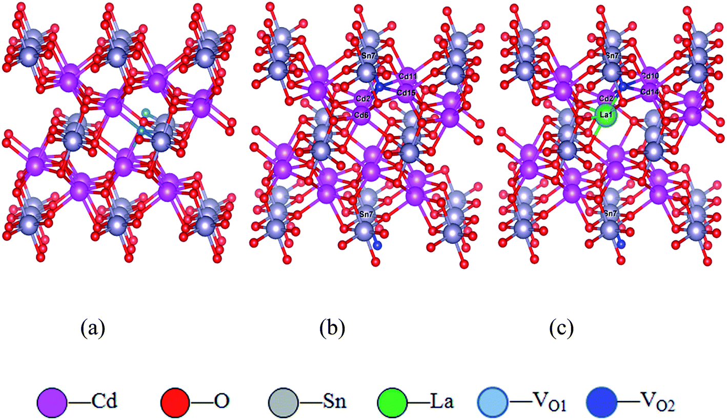 | ||
| Fig. 1 The supercell models. (a) VO1 oxygen vacancy of Cd2SnO4 supercell; (b) VO2 oxygen vacancy of Cd2SnO4 supercell; (c) La-doped Cd2SnO4 of VO2 oxygen vacancy supercell. | ||
The La doping in Cd2SnO4 has been considered in different cases, including Cd-substituted (LaCd) and charge-compensated complex 4LaCd3VSn (where V is denoted as vacancy). The calculated formation energies are 8.39, 1.58 and −3.97 eV for LaCd in charge states +1, +2, +3, respectively. The formation energy decreases as the entity charge state increases. The negative value means that LaCd3+ formation is more energetically favorable than the other native point defects formed in the host lattice. Clearly, the formation energy of LaCd3+ is the lowest, indicating that the LaCd3+ has more stable energetic configuration with local lattice relaxation. To compensate the +3 charge, a (3/4)VSn4− with opposite charge should be formed in order to keep the local neutrality. In consequence, a charge-compensated complex 4LaCd3VSn is possibly formed. The formation energy is −9.56 eV for 4LaCd3VSn.
Calculation results show that if only formation energy is considered, a charge-compensated complex 4LaCd3VSn should be most stable species after La is doped into Cd2SnO4 since its energy is the lowest among all possible types of defects. Nevertheless, the rest of defects may also become stable as temperature or the dopant concentration increases, and oxygen vacancies are easily generated in the reducing atmosphere during the preparation of oxides at high temperature. Therefore, it is necessary to investigate the coexistence of La atom and oxygen vacancies in theoretical calculations, the related research on charge compensation in unequal doping has been reported in the literature,37 so in the next calculation, we only assume one particular type of defect compensation mechanism (i.e. localised electronic compensation).
B. Bader analysis
In order to directly observe the distribution and transfer of electrons in each atom, the Bader charge analysis on the atoms around oxygen vacancy and La doping were investigated. As seen in Fig. 1, the electrotransferred from Cd and Sn atoms to O atoms in VO2 and doped systems. Table 1 shows the total charge and charge transfer of the nearest atoms of oxygen vacancy. For CTO system, O atoms are oxidized and the negative charges in O positions are −1.18. The Cd atoms and Sn atoms are reduced, and the positive charge numbers are 1.22 and 2.32 respectively. Moreover, Cd and Sn atoms are hybridized with O atoms to a certain extent, which makes the outer electrons of Cd and Sn atoms transfer to the O atoms, resulting in Cd and Sn atoms losing electrons and behaving in their reduction state, while O atoms getting electrons with oxidation state.| Materials | Atoms | Total Bader charge | Net charge number |
|---|---|---|---|
| CTO | O | 7.175 | −1.175 |
| Cd | 10.776 | 1.224 | |
| Sn | 11.683 | 2.317 | |
| O-CTO | O | 7.198 | −1.198 |
| Cd2 | 10.952 | 1.048 | |
| Cd6 | 10.952 | 1.048 | |
| Cd11 | 11.026 | 0.974 | |
| Cd15 | 11.000 | 1.000 | |
| Sn7 | 11.843 | 2.157 | |
| O-LaCTO | O | 7.210 | −1.210 |
| Cd2 | 10.982 | 1.018 | |
| Cd10 | 10.916 | 1.084 | |
| Cd14 | 10.901 | 1.099 | |
| Sn7 | 12.430 | 1.570 | |
| La | 9.017 | 1.983 |
For the VO2 oxygen vacancy of Cd2SnO4, the net charge value of the O atom varies little with an average of about −1.20. The number of electrons lost by the Cd atoms is less than that without oxygen vacancies, the transfer electrons numbers approximately equal to 1.048, 1.048, 0.97, 1.00 and the number of electrons of Sn atom lost decreases to 2.16. For the La doped of Cd2SnO4, the net charge of O atoms is −1.21, the number of electrons lost by the Cd atoms is 1.018, 1.084, 1.100, the number of electrons lost by Sn atom is 1.57 and the number of electrons lost by La atom is 1.98. After La doping, the O 2p orbital is hybridized with the La 5d orbital, a large charge transfer of 1.98e is found between La3+ and O2− in the La–O interaction. The net charge number of Sn atom is reduced, which indicates that there is a weaker interaction between Sn–O. In general, the charge analysis provides a picture of ionic interactions between the Cd, Sn cations and O anions.
C. Band structure and density of states
Using the GGA+U method, the calculated band gap value of Cd2SnO4 is 2.22 eV, which is in good accordance with the experimental band gap of the Cd2SnO4 (Eg = 2.3–2.5 eV).38,39 Thus, the theoretical value agrees well with the experimental data and the selected U values are reasonable. Fig. 2(a) shows the energy band dispersion curves along with six special k points in the Brillouin zone of Cd2SnO4. The valence band maximum (VBM) and the conduction band minimum (CBM) are located at Γ point of the Brillouin zone, which indicates that the Cd2SnO4 is a direct band-gap semiconductor. Fig. 2(b) and (c) show the band structure of the VO2 oxygen vacancy and La doped of Cd2SnO4. After the oxygen vacancy is introduced, the Fermi energy level is removed from the top of the valence band, and an impurity energy level caused by an oxygen vacancy in the forbidden zone is close to the Fermi energy level. After the introduction of La doping based on the VO2 oxygen vacancy of Cd2SnO4, the Fermi energy level enters the conduction band and overlaps with the conduction band which increases the conductivity and the band gap value increases to above 3.0 eV. The impurity energy level caused by oxygen vacancy in the forbidden zone is moved toward the valence band. The extreme values between local energy states above VBM and below CBM are placed in the different points, which means that the valence band and the local O 2p states of electronic transition can directly or indirectly move to the local Cd 4s, Sn 4d and La 5d or CBM, and these transitions lead to the change of the optical properties.40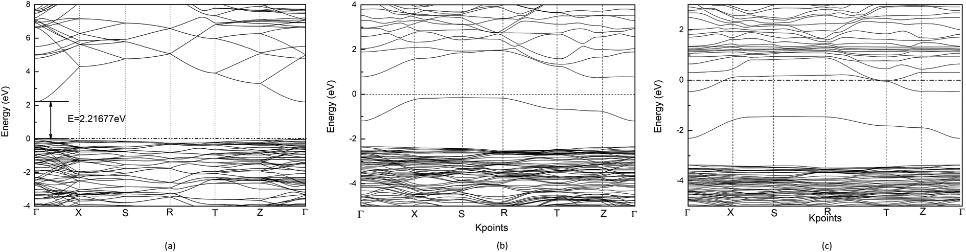 | ||
| Fig. 2 (a) The band structure of the Cd2SnO4 using the GGA+U; (b) the band structure of the VO2 oxygen vacancy of Cd2SnO4; (c) the band structure of the La doped Cd2SnO4 based on the VO2 oxygen vacancy. | ||
The total and partial density of states (DOS) of the perfect Cd2SnO4 supercell crystal is presented in Fig. 3. The conduction band is mainly composed of Cd 5s, Sn 5s and Sn 5p orbits, and the overlapping of Cd 4d with O 2p makes up the valence band top. In contrast to Cd2SnO4, for VO2 oxygen vacancy and La doped of Cd2SnO4, some new local energy levels appear in the forbidden zone. The localized energy level of the under and near conduction band is mainly composed of Cd 4s, Sn 4d and La 5d. The above and near valence bands are mainly composed of O 2p states. The local energy level caused by oxygen vacancy is mainly composed of O 2p orbital, with a very small amount of Cd 4s states. The local energy levels caused by La doped oxygen vacancy of Cd2SnO4 are mainly composed of O 2p orbitals, with a very small amount of Cd 4s, Sn 4d and La 5d states. The local energy level above the valence band influences the conductivity.41,42
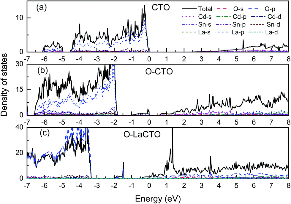 | ||
| Fig. 3 Total and partial density of states of (a) perfect Cd2SnO4 and (b) the VO2 oxygen vacancy of Cd2SnO4 and (c) La-doped Cd2SnO4 based on the VO2 oxygen vacancy, respectively. | ||
D. Optical properties
It is known that the optical properties are determined by the dielectric function ε(ω) = ε1(ω) + iε2(ω), which is mainly contributed from the electronic structures.43,44 The real part of this function, ε1(ω) represents the dispersion of the incident photons by the materials, while the imaginary part ε2(ω) results from the inter-band transition between the occupied state below Fermi level and the unoccupied state above top Fermi level due to the photon absorption. The real part of dielectric function ε1(ω) can be evaluated from imaginary part ε2(ω) through Kramer–Kronig relationship, where ε2(ω) can be treated as detailing the real transitions between occupied and unoccupied electronic states for any materials.45–48 All other optical constants, such as the absorption coefficient, refractive index and reflectivity can be derived from ε1(ω) and ε2(ω).Therefore, the imaginary part of the dielectric function ε2(ω) of perfect and VO2 oxygen vacancy and La doped of Cd2SnO4 is calculated, which is presented in Fig. 4. Considering the tensor nature of the dielectric function, the imaginary parts of the dielectric function are averaged over three polarization vectors (x, y, and z) in our calculations. The peaks of the imaginary part of the dielectric function are related to the electron excitation. From Fig. 4, it can be seen that there are two major peaks located at 7.70 and 10.24 eV for perfect Cd2SnO4. Combined with the density of states and electronic band structure analysis, the peaks in perfect Cd2SnO4 are mainly owing to the contribution of the direct electron transitions between the O 2p states in the upper valence band and Cd 4d, Sn 4s states in the conduction band. As for VO2 oxygen vacancy and La doped of Cd2SnO4, the trend is similar with perfect Cd2SnO4, the main peaks of the VO2 oxygen vacancy of Cd2SnO4 locate at 1.80, 2.30, 10.10 and 15.76 eV. In the visible part there are two new peak positions of 1.8 and 2.3 eV, respectively. The first peak mainly comes from within the O 2p local energy states in forbidden band transition to the conduction band; and the second peak is caused by the valence band O 2p state transition to the conduction band. After the doped La atom, the main peaks are located at 2.00, 9.31 and 14.28 eV. The new peak in the visible part of the spectrum is at 2.0 eV, and the peak value is smaller compared with the VO2 oxygen vacancy of Cd2SnO4. A new peak is also found in the low energy around 0.40 eV for the La-doped is originated by the excitation of O 2p electron from the top of valence band to the impurity energy level which is located at the bottom of the conduction band. Because of the introduction of local energy level, the electron transition between the deep valence band and the conduction band decreases, while the electron transition between the local energy level and the conduction band increases.
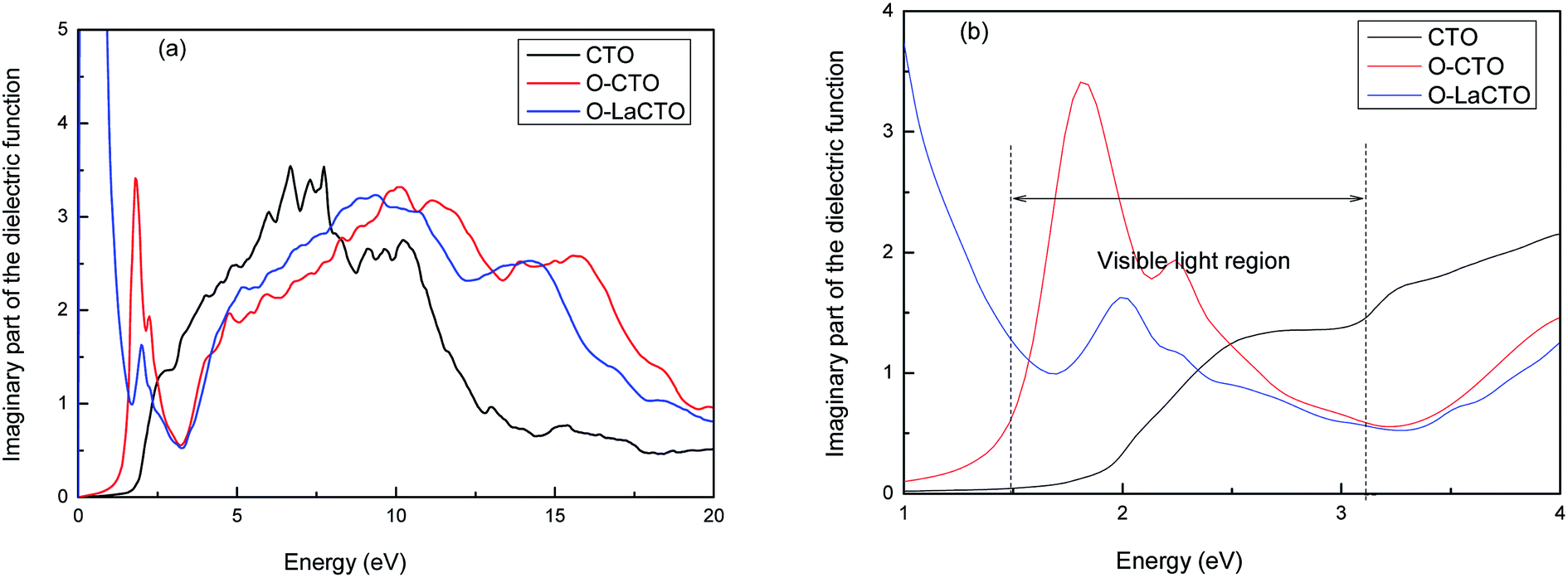 | ||
| Fig. 4 The imaginary part of the dielectric function of perfect and VO2 oxygen vacancy and La doped of Cd2SnO4 (a); the visible light region part (b). | ||
Transparent conducting materials require low absorption and reflectivity coefficient but high transmittance in the visible light region, so we calculated the absorption, reflectivity, refractive and transmittance. As is shown in Fig. 5(a), the absorption edge of perfect Cd2SnO4 in the visible light region is about 500 nm, which is in conformity with experimental studies, while the optical absorption edge is about 800 nm for VO2 oxygen vacancy of Cd2SnO4 which is red shifted compare with the perfect Cd2SnO4. Oxygen vacancy enables the conduction band to move towards the lower energy, so that the electron transition can be completed by absorbing only a smaller amount of energy, which eventually leads to the tendency of the absorption spectrum to move to the lower energy (red shift). After the doping of the La atom, the optical absorption coefficient decreases in the visible light region but increases in the infrared region compare with VO2 oxygen vacancy of Cd2SnO4. The reason why La doped Cd2SnO4 increases the absorption in infrared region is that the occupied states close to CBM are shallow donor states, and when the electrons in the local energy level transit to the bottom of the conduction band, these states induce a significant absorption in IR region.
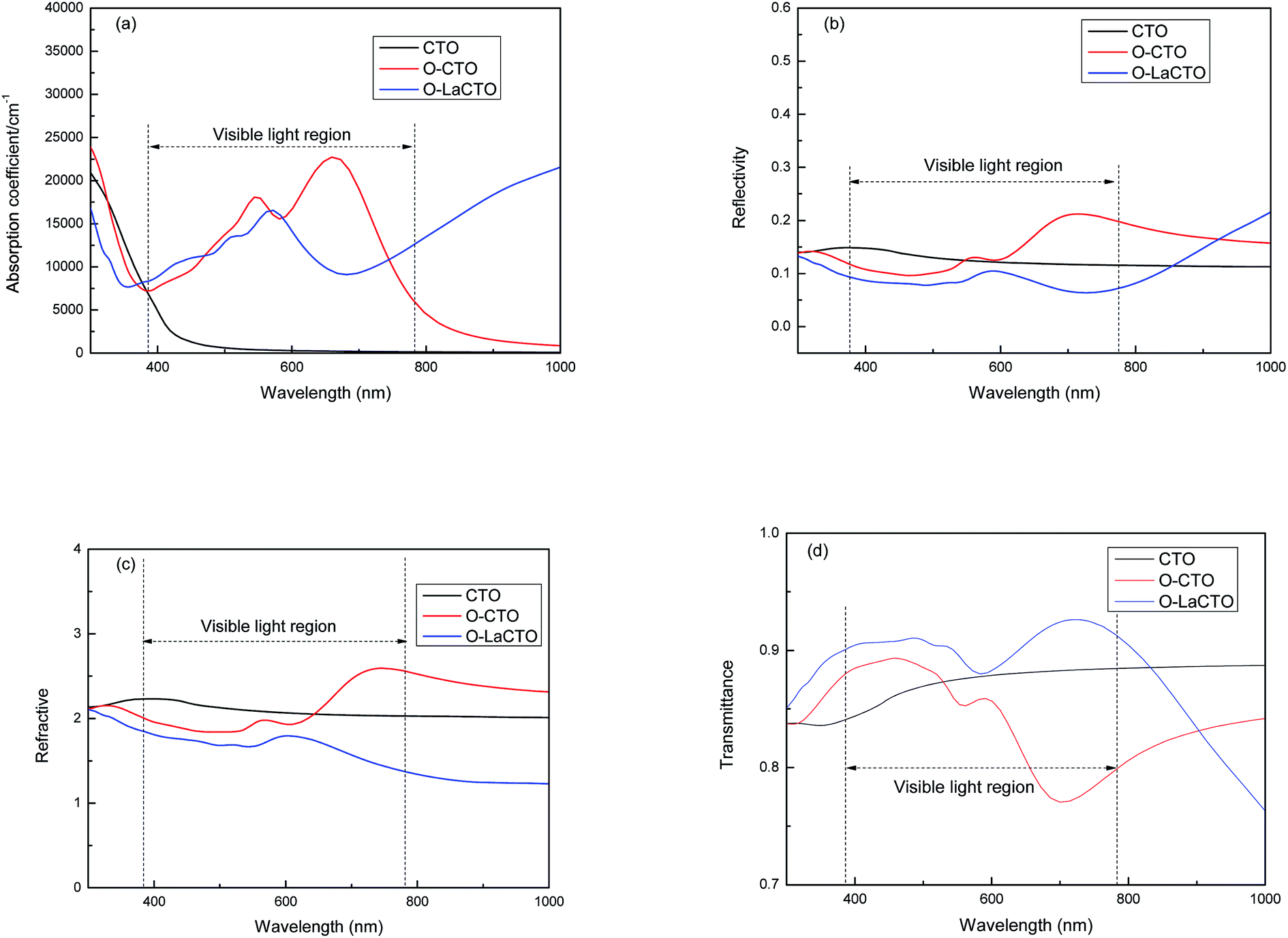 | ||
| Fig. 5 The variation of the (a) absorption, (b) reflectivity, (c) refractive and (d) transmittance as a function of the wavelength of perfect and VO2 oxygen vacancy and La doped of Cd2SnO4. | ||
In the visible light region of the spectrum as is shown in Fig. 5(b), it is clear that the perfect Cd2SnO4 has a low reflectivity (less than 15%) in the visible and IR regions. However, this reflectivity is decreased in short wavelength (<600 nm) in visible light region and is significantly increased in long wavelength (>600 nm) up to infrared region for VO2 oxygen vacancy of Cd2SnO4. The reflectivity is the smallest (less than 10%) after doping La atom. As for the refractive index, the trend is similar with reflectivity, as is shown in Fig. 5(c). The refractive index of CTO is about 2.1, and in the short wavelength (<600 nm) for VO2 oxygen vacancy of Cd2SnO4 the refractive index decreases. After La doping, the refractive index further decreases and the average value is 1.4.
The average transmittance (T) equals to 100% subtract the average reflectance (R) and average absorption (A) (T = 100% − R − A). From Fig. 5(d) it can be concluded that the transmittance of CTO in the visible light region is about 85%. The transmittance of the VO2 oxygen vacancy of Cd2SnO4 is increased in short wavelength (<600 nm) in visible light region but significantly decreased in long wavelength (>600 nm). After La doped, the transmittance increased to about 90% compared with CTO and VO2 oxygen vacancy of Cd2SnO4. It is indicated that the presence of oxygen vacancies is not conducive to the enhancement of the optical properties of transparent conducting materials. Therefore, it is necessary to control the occurrence of oxygen vacancies in the experiment and increase the transmittance by doping different atoms.
IV. Conclusions
The electronic structure and optical properties of oxygen vacancy and La-doped Cd2SnO4 were calculated using the GGA+U method based on the first principles calculations. It was found that the impurity levels appeared in the forbidden band for Cd2SnO4 with oxygen vacancies, and the impurity levels caused by oxygen vacancy mainly were composed by O 2p orbital, mixed with a small amount of Cd 4s orbital. After La doping, the Fermi level entered the conduction band, overlapping with the conduction band and the conductivity being improved. The results of Bader charge analysis showed that there was a slightly stronger interaction between La and O atoms but a weaker interaction between Sn and O atoms after La atom doping. The results of optical performance analysis showed that the transmittance caused by oxygen vacancy increased in short wavelength but decreased in long wavelength up to infrared region, and the transmittance of La atom doping increased in visible light region compared with Cd2SnO4. Therefore, it was necessary to increase the transmittance by doping different atoms in the experiment.Conflicts of interest
There are no conflicts to declare.Acknowledgements
This project was financially supported by the National Natural Science Foundation of China under Grants 51672014.References
- D. S. Ginley and C. Bright, MRS Bull., 2000, 25, 15–18 CrossRef CAS.
- T. Minami, MRS Bull., 2000, 25, 38–44 CrossRef CAS.
- T. J. Coutts, D. L. Young and X. N. Li, MRS Bull., 2000, 25, 58–65 CrossRef CAS.
- A. J. Smith, Acta Crystallogr., 1960, 13, 749–752 CrossRef CAS.
- A. J. Nozik, Phys. Rev. B: Condens. Matter Mater. Phys., 1972, 6, 453–459 CrossRef CAS.
- X. Wu, R. Ribelin, R. G. Dhere, D. S. Albin, T. A. Gessert, S. Asher, D. H. Levi, A. Mason, H. R. Moutinho and P. Sheldon, Proceedings of the 28th IEEE Photovoltaic Specialists Conference, IEEE, 2000, pp. 470–474 Search PubMed.
- X. Z. Wu, Sol. Energy, 2004, 77, 803–814 CrossRef CAS.
- A. W. Metz, M. A. Lane, C. R. Kannewurt, K. R. Poeppelmeier and T. J. Marks, Chem. Vap. Deposition, 2004, 6, 297–300 CrossRef.
- R. A. Ismail, S. A. Tawfiq, R. Hababa, R. S. Sabry and O. A. Abdulraza, e-J. Surf. Sci. Nanotechnol., 2007, 5, 152–154 CrossRef CAS.
- R. Kumaravel, V. Krishnakumar, V. Gokulakrishnan, K. Ramamurthi and K. Jeganathan, Thin Solid Films, 2010, 518, 2271–2274 CrossRef CAS.
- C. J. D. Godines, C. G. T. Castanedo, R. C. Pérez, G. T. Delgado and O. Z. Ángel, Sol. Energy Mater. Sol. Cells, 2014, 128, 150–155 CrossRef.
- B. Schumm, P. Wollmann, J. Fritsch, J. Grothe and S. Kaskel, J. Mater. Chem., 2011, 21, 10697–10704 RSC.
- H. M. Ali, H. A. Mohamed, M. M. Wakkad and M. F. Hasaneen, Jpn. J. Appl. Phys., 2009, 48, 041101 CrossRef.
- N. Miyata, K. Miyake and S. Nao, Thin Solid Films, 1979, 58, 385–389 CrossRef CAS.
- N. Miyata, K. Miyake and Y. Yamaguchi, Appl. Phys. Lett., 1980, 37, 180–182 CrossRef CAS.
- A. M. Al-Baradi, M. M. El-Nahass, M. M. A. El-Raheem, A. A. Atta and A. M. Hassanien, Radiat. Phys. Chem., 2014, 103, 227–233 CrossRef CAS.
- M. M. El-Nahass, A. A. Atta, M. M. A. El-Raheem and A. M. Hassanien, J. Alloys Compd., 2014, 585, 1–6 CrossRef CAS.
- R. Mamazza Jr, D. L. Morel and C. S. Ferekides, Thin Solid Films, 2005, 484, 26–33 CrossRef.
- K. Jeyadheepan, M. Thamilselvan, K. Kim, J. Yi and C. Sanjeeviraja, J. Alloys Compd., 2015, 620, 185–191 CrossRef CAS.
- S. M. Al-Sofiany and H. E. Hassan, J. Alloys Compd., 2015, 651, 149–156 CrossRef CAS.
- S. H. Lee, E. W. Lee, S. Y. Park and C. W. Jeon, Mol. Cryst. Liq. Cryst., 2010, 532, 106–111 Search PubMed.
- D. L. Peng, S. R. Jiang and W. L. Wang, Chin. Phys. Lett., 1993, 10, 189–192 CrossRef CAS.
- W. L. Wang, K. J. Liao, C. Z. Cai, G. B. Liu and Y. Ma, Surf. Coat. Technol., 2003, 167, 284–287 CrossRef CAS.
- S. Y. Sun, J. L. Huang and D. F. Lii, J. Mater. Res., 2005, 20, 2030–2037 CrossRef CAS.
- T. J. Coutts, D. L. Young, X. Li and X. Wu, J. Vac. Sci. Technol., A, 2000, 18, 2646–2660 CAS.
- T. Stapiński, E. Leja and T. Pisarkiewicz, J. Phys. D: Appl. Phys., 1984, 17, 407–413 CrossRef.
- G. Haacke, W. E. Mealmaker and L. A. Siegel, Thin Solid Films, 1978, 55, 67–81 CrossRef CAS.
- G. Kresse and J. Furthmuller, Phys. Rev. B: Condens. Matter Mater. Phys., 1996, 54, 11169–11186 CrossRef CAS.
- G. Kresse and J. Furthmuller, Comput. Mater. Sci., 1996, 6, 15–50 CrossRef CAS.
- J. P. Perdew, K. Burke and M. Ernzerhof, Phys. Rev. Lett., 1996, 77, 3865–3868 CrossRef CAS PubMed.
- G. Kresse and D. Joubert, Phys. Rev. B: Condens. Matter Mater. Phys., 1999, 59, 1758–1775 CrossRef CAS.
- H. J. Monkhorst and J. D. Pack, Phys. Rev. B: Condens. Matter Mater. Phys., 1976, 13, 5188–5192 CrossRef.
- X. G. Ma, Y. Wu, Y. H. Lv and Y. F. Zhu, J. Phys. Chem. C, 2013, 117, 26029–26039 CAS.
- S. J. Wang, X. B. Shi and J. M. Li, RSC Adv., 2016, 6, 107865–107870 RSC.
- X. L. Huang, J. Lv, Z. S. Li and Z. G. Zhou, ChemInform, 2010, 41, 341–344 Search PubMed.
- C. G. Van de Walle and J. Neugebauer, J. Appl. Phys., 2004, 95, 3851–3879 CrossRef CAS.
- J. Han, L. J. Li, M. Y. Peng, B. L. Huang, F. J. Pan, F. W. Kang, L. Y. Li, J. Wang and B. F. Lei, Chem. Mater., 2017, 29, 8412–8424 CrossRef CAS.
- G. M. Zhang, Z. Y. Fu, Y. C. Wang, H. Wang and Z. Xie, RSC Adv., 2015, 5, 83922–83930 RSC.
- S. Dinesh, M. Anandan, V. K. Premkumar, S. Barathan, G. Sivakumar and N. Anandhan, Mater. Sci. Eng., B, 2016, 214, 37–45 CrossRef CAS.
- D. Steiauf, J. L. Lyons, A. Janotti and C. G. Van de Walle, APL Mater., 2014, 2, 52 Search PubMed.
- A. Janotti and C. G. Van de Walle, Appl. Phys. Lett., 2005, 87, 122102 CrossRef.
- M. Choi, A. Janotti and C. G. Van de Walle, J. Appl. Phys., 2013, 113, 044501 CrossRef.
- A. Slassi, Optik, 2015, 126, 4751–4756 CrossRef CAS.
- J. F. Guo, W. Zhou, P. F. Xing, P. Q. Yu, Q. G. Song and P. Wu, Solid State Commun., 2012, 152, 924–928 CrossRef CAS.
- S. A. Kelkar, P. A. Shaikh, P. Pachfule and S. B. Ogale, Energy Environ. Sci., 2012, 5, 5681–5685 CAS.
- A. Slassi, S. Naji, A. Benyoussef, M. Hamedoun and A. El Kenz, J. Alloys Compd., 2014, 605, 118–123 CrossRef CAS.
- R. S. Zhang, Y. Liu, Q. Gao, F. Teng, C. L. Song, W. Wang and G. R. Han, J. Alloys Compd., 2011, 509, 9178–9182 CrossRef CAS.
- H. Y. Yan, Y. R. Guo, Q. G. Song and Y. F. Chen, Phys. B, 2014, 434, 181–184 CrossRef CAS.
| This journal is © The Royal Society of Chemistry 2018 |