DOI:
10.1039/C7RA10425A
(Paper)
RSC Adv., 2018,
8, 10828-10835
ZnO/MoX2 (X = S, Se) composites used for visible light photocatalysis
Received
20th September 2017
, Accepted 8th March 2018
First published on 19th March 2018
Abstract
Hybrid density functional has been adopted to investigate the structural, electronic, and optical properties of ZnO/MoS2 and ZnO/MoSe2 composites as compared with the results of ZnO, MoS2, and MoSe2 monolayers. The results indicate that MoS2 and MoSe2 monolayers could contact with monolayer ZnO to form ZnO/MoS2 and ZnO/MoSe2 heterostructures through van der Waals (vdW) interactions. The calculated bandgap of ZnO/MoS2 (ZnO/MoSe2) is narrower than that of ZnO or MoS2 (MoSe2) monolayers, facilitating the shift of light absorption edges of the composites towards visible light in comparison with bare ZnO and MoX2 monolayers. Through the application of strain, the ZnO/MoS2 and ZnO/MoSe2 composites which own suitable bandgaps, band edge positions, efficient charge separation, and good visible light absorption will be promising for visible light photocatalytic water splitting. These results provide a route for design and development of efficient ZnO/MoS2 and ZnO/MoSe2 photocatalysts for water splitting.
1 Introduction
Monolayer MoS2 has drawn much attention owing to its intriguing electronic, optical, and mechanical properties, and MoS2 monolayer could be peeled off from the bulk or grown by chemical vapor deposition,1,2 similar to the methods for graphene production. MoS2 monolayer is a direct bandgap semiconductor with the bandgap of 1.90 eV,3 which makes it favorable for visible light absorption. Therefore, many studies have focused on the photocatalytic water splitting of monolayer MoS2 under visible light irradiation.4,5 Due to its layered nature and high surface energy, MoS2 monolayers tend to stack together through π–π interaction during the preparation process. This would block a substantial amount of catalytic edge sites, resist the electron transfer and molecules diffusion, and retard the catalytic reaction.6,7 For effective photocatalytic water splitting, the valence and conduction bands for semiconductors must straddle the water redox levels, i.e., the conduction band minimum (CBM) must be higher than the water reduction potential and the valence band maximum (VBM) must be lower than the water oxidation potential.8,9 As additional overpotential associated with each electron transfer and gas evolution steps in the process of photocatalytic water splitting, a bandgap larger than 1.23 eV is demanded for effective photocatalysis.10,11 To achieve high photocatalytic activity, the MoS2 monolayer should be tuned with its bandgap larger than 1.23 eV and band edge positions straddling the water redox levels.
Substantial MoS2-based composites, such as MoS2/BiVO4,12 MoS2/Ag3PO4,13 MoS2/SrZrO3,14 MoS2/Cu2O,15 MoS2/CdS,16 MoS2/TiO2,17 MoS2/SnO2,18 MoS2/Bi2S3,19 MoS2/g-C3N4,20,21 and MoS2/graphene22 etc. have been found experimentally to extend the absorption of light to visible light region and exhibit higher visible photocatalytic activities for water splitting or organic degradation as compared to MoS2. In particular, recent experimental report23 suggests that MoS2/ZnO exhibits higher photocatalytic efficiency in degradation of methylene blue as compared to the pure MoS2. Another experiment24 has reported the MoS2 nanosheet-coated ZnO heterostructure could be successfully fabricated through a simple hydrothermal method, and the 1.00 wt% MoS2/ZnO composite has shown obviously higher photocatalytic activity for water splitting as compared to that of pure ZnO as the hydrogen production rate of MoS2/ZnO composite is 14.8 times higher than that of pure ZnO. Some studies have reported that the graphene-like ZnO nanosheet25–27 has been successfully prepared and exhibits excellent photocatalytic activity. We may wonder that if the two dimensional ZnO/MoS2 composite consisting of a ZnO monolayer and a MoS2 monolayer will be suitable photocatalyst for water splitting, but there in no related experimental and theoretical report. The photocatalytic properties of two-dimensional ZnO/MoS2 composite remains unclear, as the electronic structures including density of states (DOS), band structures, charge transfer, and interface interaction have not been comprehensively studied. The redox ability of two-dimensional ZnO/MoS2 heterostructure may be influenced by the valence and conduction band edge positions, which will change with the Fermi level change before and after MoS2 and ZnO monolayers contacting with each other. These have not been studied. Therefore, to understand the photocatalysis properties of ZnO/MoS2 heterostructure, these problems mentioned earlier should been investigated. Besides, as the geometric and electronic structures of MoSe2 is similar to those of MoS2, we wonder if the construction of heterostructure between MoSe2 and ZnO monolayers will improve the photocatalytic activity of MoSe2.
In this work, the structural, electronic, and optical properties of two dimensional ZnO/MoS2 and ZnO/MoSe2 heterostructures have been calculated in contrast with those of ZnO, MoS2, and MoSe2 monolayers to investigate whether or not the ZnO/MoSe2 will exhibit high visible photocatalytic activity on hydrogen production. The structure of this work is organized as follows. Section 2 displays the computational method and details we adopted in this study, while Section 3 gives the calculated results and discussion about the structural, electronic, and optical properties of ZnO/MoS2 and ZnO/MoSe2 heterostructures, and finally some concluding remarks based on the calculated results are offered in Section 4.
2 Computational details
The geometric model of the ZnO/MoS2 (ZnO/MoSe2) heterostructure is constructed by loading a 2 × 2 supercell of ZnO monolayer on a 2 × 2 supercell of MoS2 (MoSe2) monolayer. The thickness of vacuum space of 18 Å between neighboring nanocomposites has been adopted to avoid their interactions. For convenience, all the heterojunction models are fixed to the same lattice constants (a = b = c = 6.58 Å) as those of optimized 2 × 2 supercell of ZnO monolayer. All the density functional calculations by utilization of generalized gradient approximation (GGA)28 of the Perdew–Burke–Ernzerhof (PBE)29 form to treat the exchange correlation contribution have been performed in the Vienna ab initio simulation (VASP) package.30 The projected augmented wave (PAW)31 method has been adopted to describe the pseudo-potential, and the valence states adopted for construction the PAW potentials are Zn (3d104s2), Mo (4p65s24d4), O (2s22p4), S (3s23p4), and Se (4s24p4). In addition, the DFT-D3 (ref. 32) van der Waals (vdW) correction proposed by Grime is utilized to describe the weak vdW interactions. The Heyd–Scuseria–Ernzerhof (HSE06)33,34 hybrid density functional with 25% Hartree–Fock exchange energy has been utilized to obtain accurate electronic structures. The energy cutoff of 500 eV, the energy convergence tolerance of 1.0 × 10⁻⁵ eV, the convergence thresholds for atomic force of 10−2 eV Å−1, and the k-point of 13 × 13 × 1 for 1 × 1 unit of ZnO and MX2 monolayers and 7 × 7 × 1 for 2 × 2 units of ZnO/MX2 systems are found sufficient for geometrical optimization and electronic structure calculations. Finally, the absorption curves are obtained from the imaginary part of the dielectric constant by utilization of Kramers–Kronig dispersion relation.35 In addition, the absolute band edge positions with reference to the vacuum level are obtained through shifting the band structure by subtracting the calculated vacuum level through averaging the LOCPOT file along the specified plane.
3 Results and discussion
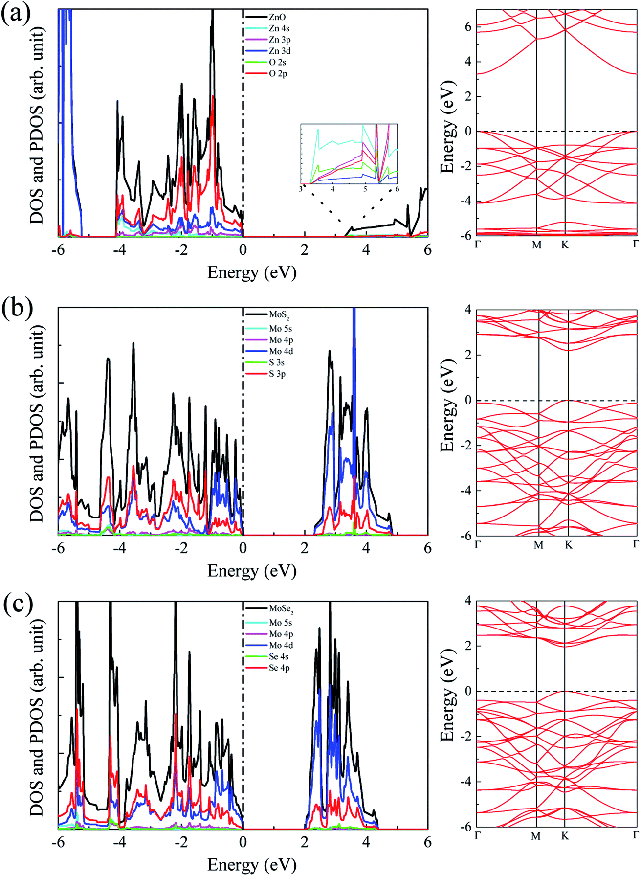
The calculated lattice constants for ZnO, MoS2, and MoSe2 monolayers are respectively 3.290, 3.174, and 3.304 Å, the calculated Zn–O, Mo–S, and Mo–Se bond lengths are respectively 1.900, 2.413, and 2.540 Å, and the obtained bandgaps for ZnO, MoS2, and MoSe2 monolayers by utilization of HSE06 with the mixing coefficient of 25% are respectively 3.30, 2.20, and 1.90 eV. These results are in good agreement with the previous studies.36–38 The small lattice mismatch of −3.5% (+0.4%) between ZnO and MoS2 (MoSe2) makes it beneficial for construction of ZnO/MoS2 (ZnO/MoSe2) composite. The electronic properties including DOS, project density of states (PDOS), and band structures of ZnO, MoS2, and MoSe2 monolayers are depicted in Fig. 1. ZnO monolayer is a direct bandgap semiconductor with the VBM and CBM locating at the same k-point of Γ, and the MoS2 and MoSe2 monolayers are also direct bandgap semiconductors with the VBM and CBM locating at the same k-point of K. The VBM of monolayer ZnO is mainly contributed by Zn 3d and O 2p states, whereas the CBM is comprised of Zn 4s. For monolayer MoS2, the VBM is dominated by the mixing of Mo 4d and S 3p states, and the CBM mainly originates from Mo 4d states. For the case of monolayer MoSe2, the VBM is predominately composed of Mo 4d and Se 4p states, whereas the CBM mainly originates from Mo 4d states.
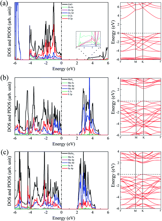 |
| | Fig. 1 DOS, PDOS, and band structures for (a) ZnO, (b) MoS2, and (c) MoSe2 monolayers. The Fermi level is set to zero. | |
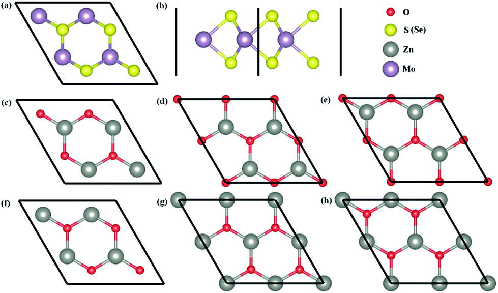
The top and side views of MoS2 (MoSe2) monolayers are shown in Fig. 2a and b, and six possible configurations of ZnO monolayers with the rotation angles of 0°, 60°, 120°, 180°, 240°, and 300° are considered to establish six possible models of ZnO/MoS2 (ZnO/MoSe2) composites with the MoS2 (MoSe2) monolayer. For convenience, these heterostructures are called as ZnO/MoS2 (ZnO/MoSe2) (i), (ii), (iii), (iv), (v), and (vi). Table 1 lists the calculated total energy difference between various configurations and the lowest energy configuration, the interlayer distances between ZnO and MoS2 (MoSe2) layers, the Zn–O and Mo–S (Mo–Se) bond lengths for monolayers and heterostructures. The energy difference ΔE is the total energy difference between the different ZnO/MoS2 (ZnO/MoSe2) configurations and the most stable configuration:
 |
| | Fig. 2 Schematic views of MoS2 (MoSe2) monolayer (a) and (b) and various ZnO monolayers (c)–(h) with different rotation angles. When the rotation angle of configuration (c) is set to be 0°, then the rotations for the rest of configurations are (d) 60°, (e) 120°, (f) 180°, (g) 240°, and (h) 300°. | |
Table 1 Calculated energy difference ΔE (eV) between various configurations and the lowest energy configuration, the layer distance d (Å) for ZnO/MoS2 (ZnO/MoSe2) composites, the Zn–O and Mo–S (Mo–Se) bond lengths for monolayers and composites
| Systems |
ΔE (eV) |
Layer distance (Å) |
LZn–O (Å) |
LMo–S(Mo–Se) (Å) |
| ZnO |
|
|
1.900 |
|
| MoS2 |
|
|
|
2.412 |
| MoSe2 |
|
|
|
2.540 |
| ZnO/MoS2 (i) |
0.035 |
2.900 |
1.900 |
2.436 (2.440) |
| ZnO/MoS2 (ii) |
0.002 |
2.831 |
1.900 |
2.435 (2.440) |
| ZnO/MoS2 (iii) |
0 |
2.870 |
1.900 |
2.437 (2.440) |
| ZnO/MoS2 (iv) |
0.309 |
3.290 |
1.900 |
2.439 (2.440) |
| ZnO/MoS2 (v) |
0.321 |
3.286 |
1.900 |
2.439 (2.440) |
| ZnO/MoS2 (vi) |
0.047 |
2.931 |
1.900 |
2.438 (2.440) |
| ZnO/MoSe2 (i) |
0.049 |
3.025 |
1.900 |
2.533 (2.538) |
| ZnO/MoSe2 (ii) |
0.048 |
2.979 |
1.900 |
2.531 (2.538) |
| ZnO/MoSe2 (iii) |
0 |
3.010 |
1.900 |
2.534 (2.538) |
| ZnO/MoSe2 (iv) |
0.273 |
3.358 |
1.900 |
2.537 (2.537) |
| ZnO/MoSe2 (v) |
0.279 |
3.354 |
1.900 |
2.537 (2.537) |
| ZnO/MoSe2 (vi) |
0.014 |
3.028 |
1.900 |
2.537 (2.537) |
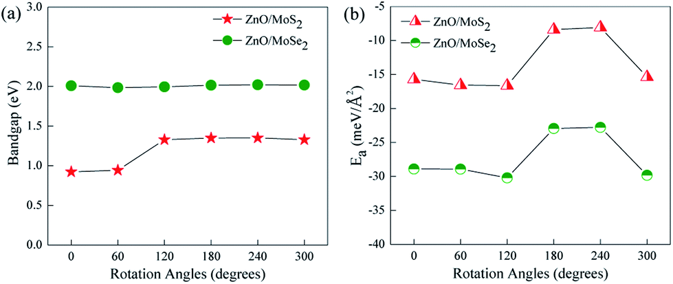
The most stable configurations for ZnO/MoS2 and ZnO/MoSe2 with ΔE = 0 are both configuration (iii), which is quite similar to the case of MoS2/GaN heterostructure but quite different from the case of MoS2/AlN heterostructure.39 The lowest energy configurations of ZnO/MoS2 and ZnO/MoSe2 do not have the smallest interlayer distances, which is quite different from the cases of MoS2/AlN and MoS2/GaN heterostructures39 where the lowest energy structure has the smallest interlayer distance. Herein ZnO/MoS2 (ii) and ZnO/MoSe2 (ii) have the smallest interlayer distances. For all the configurations, the Zn–O bond length in ZnO/MoS2 and ZnO/MoSe2 composites are all 1.900 Å, as all the lattice constants of a, b are fixed as the values of 2 × 2 supercell of ZnO monolayer in our calculations and in the heterostructures the ZnO layer is almost unaffected by the MoS2 and MoSe2 layers due to the weak vdW interactions. In ZnO/MoS2 composite the Mo–S bond length is slightly larger than that in MoS2 monolayer while in ZnO/MoSe2 composite the Mo–Se bond length is lightly smaller than that in MoSe2 monolayer. These differences of Mo–S and Mo–Se bond lengths in heterostructures and monolayers are due to the small atomic adjustments to accommodate the strain energy caused by the lattice mismatch. Nevertheless, the bond length changes are very small, suggesting there only small rearrangements in the heterostructures. It should be mentioned that practically there could be some rotational component to the stacking in order to accommodate the small strain energy. It could be seen from Fig. 3a, the bandgaps of ZnO/MoS2 composites with the rotational angles of 0° and 60° are quite different from those of ZnO/MoS2 composites with the rotational angles of 120°, 180°, 240°, and 300°, which suggests that the rotational component has some impact on the electronic structures of ZnO/MoS2 composites. However, the bandgaps of ZnO/MoSe2 composites does not change with the rotation angle changes, which means that the rotational component has almost no affect on the electronic structures of ZnO/MoSe2 composites because of the weak vdW interaction between ZnO and MoSe2 layers.
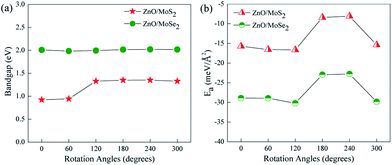 |
| | Fig. 3 (a) Varied bandgaps and (b) interface adhesion energies (Ea) for ZnO/MoS2 and ZnO/MoSe2 composites with different rotation angles. | |
To discuss the relative stability of these heterostructures, the interface adhesion energies are calculated by the following relationship:
| | |
Ea = [EZnO/MoS2(MoSe2) − EZnO − EMoS2(MoSe2)]/S
| (2) |
where
EZnO/MoS2(MoSe2),
EZnO, and
EMoS2(MoSe2) are the total energies of optimized ZnO/MoS
2 (ZnO/MoSe
2) heterostructures, monolayer ZnO, monolayer MoS
2 (MoSe
2), and
S denotes the area of the heterostructure supercell perpendicular to
z direction. The interface adhesion energies of ZnO/MoS
2 and ZnO/MoSe
2 heterostructures with different rotation angles are displayed in
Fig. 3b, the change trends of interface adhesion energies for ZnO/MoS
2 and ZnO/MoSe
2 heterostructures are almost the same. ZnO/MoS
2 (iii) and ZnO/MoSe
2 (iii) respectively have the smallest interface adhesion energies of −16.63 and −30.20 meV Å
−2 in the corresponding heterostructures, and the negative values suggest that these two interface formations are exothermic and could be easily obtained. Furthermore, these two interface adhesion energies are very close to the type vdW interface adhesion energy of around −20 meV Å
−2 by the DFT calculation,
40 implying that both ZnO/MoS
2 and ZnO/MoSe
2 composites are vdW heterostructures. The latter calculation and discussion are focused on the heterostructures of ZnO/MoS
2 (iii) and ZnO/MoSe
2 (iii) which are energetically more favorable in the considered configurations.
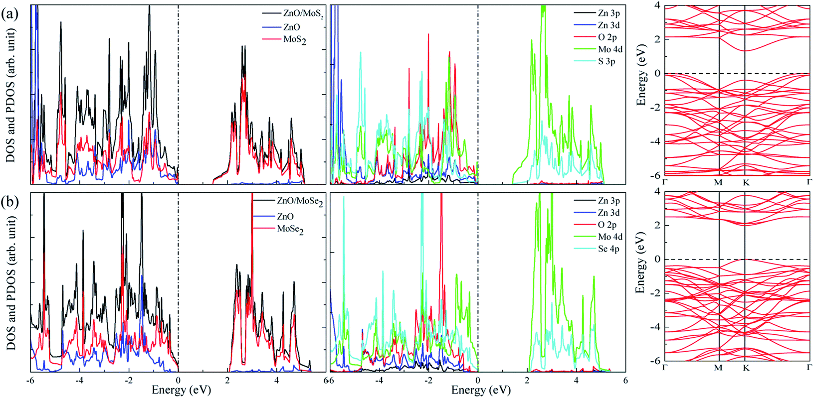
The band structures for ZnO/MoS2 and ZnO/MoSe2 are plotted in Fig. 4a and b, the obtained bandgaps for ZnO/MoS2 and ZnO/MoSe2 are respectively 1.33 and 2.01 eV. The ZnO/MoS2 is an indirect bandgap semiconductor with VBM locating at the k-point around Γ and CBM locating at the k-point of K, while the ZnO/MoSe2 is a direct bandgap semiconductor with VBM and CBM locating at the same k-point of K. The DOS and PDOS of ZnO/MoS2 and ZnO/MoSe2 are depicted in Fig. 4a and b. For the ZnO/MoS2 composite, the top of the valence band is contributed by the mixing of Mo 4d, O 2p, Zn 3d, S 3p, and Zn 3p states, whereas the bottom of the conduction band is mainly comprised of Mo 4d and S 3p states. Under light irradiation, the electrons below the Fermi level will absorb photo energy and jump to the conduction band. Considering the electronic transition of angular momentum selection rules (Δl = ±1), the electrons mainly jump from O 2p states to Mo 4d states, which means that during the photocatalysis process the photoexcited electrons will transfer from ZnO layer to MoS2 layer. The water oxidation process mainly happens in the ZnO layer, whereas the water reduction process mainly takes place in MoS2 layer. These will facilitate the electron–hole separation and achieve efficient photocatalysis. For ZnO/MoSe2 system, the VBM is mainly contributed by Mo 4d and Se 4p states, whereas the CBM is dominated by Mo 4d and Se 4p states. Under light irradiation most electrons under the Fermi level jump from Mo 4d (Se 4p) states to Se 4p (Mo 4d) states.
 |
| | Fig. 4 DOS, PDOS, and band structures for (a) ZnO/MoS2 and (b) ZnO/MoSe2 composites. | |
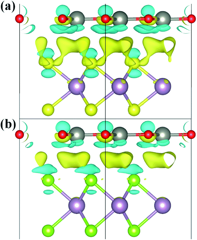
To explore the charge redistribution across the ZnO/MoS2 (MoSe2) heterostructures, the charge density differences (Δρ) are obtained by the following relationship:
| | |
Δρ = ρZnO/MoS2(MoSe2) − ρZnO − ρMoS2(MoSe2)
| (3) |
where
ρZnO/MoS2(MoSe2),
ρZnO, and
ρMoS2(MoSe2) are respectively the charge densities of ZnO/MoS
2(MoSe
2) composites, monolayer ZnO, and monolayer MoS
2(MoSe
2). The three-dimensional charge density differences of ZnO/MoS
2 and ZnO/MoSe
2 composites are plotted in
Fig. 5, where the yellow and cyan regions respectively indicate charge accumulation and depletion. The charge redistribution mostly happens at the ZnO layer and the side of MoS
2 (MoSe
2) which is adjacent to the ZnO layer, while there is almost no charge transfer on the side of MoS
2 (MoSe
2) far away from the interface because of the weak interaction between them. Generally, both the charge depletion and accumulation constitute the interface charge redistribution behavior between the ZnO and MoS
2 (MoSe
2) layers, which causes the interface electric dipole formation and promote the electron–hole separation. The Bader analysis also indicates that the electrons transfer from the ZnO side to MoS
2 (MoSe
2) side across the interface.
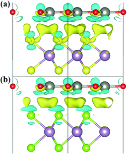 |
| | Fig. 5 Side views of the charge density differences of (a) ZnO/MoS2 and (b) ZnO/MoSe2 composites. The yellow region represents charge accumulation and the cyan region indicates charge depletion; the isosurface value is 0.0003 e bohr−3. | |
Generally, the optical absorption properties of the photocatalysts closely related to their electronic structures are also important to affect the photocatalytic activity. The optical absorbance curves of ZnO, MoS2, MoSe2 monolayers, ZnO/MoS2, and ZnO/MoSe2 composites are plotted in Fig. 6a. The large bandgap of monolayer ZnO limits the monolayer ZnO only response to ultraviolet light, whereas MoS2 and MoSe2 monolayers absorb visible light because of their narrow bandgaps. The optical absorbance edge of the ZnO/MoS2 composite moves to a longer wavelength region in contrast with those of ZnO and MoS2 monolayers. The visible light absorption of ZnO/MoSe2 composite is not improved as compared to the MoSe2 monolayer but obviously enhanced in contrast with the ZnO monolayer. Besides, the formation of ZnO/MoS2 (ZnO/MoSe2) composites will prevent the MoS2(MoSe2) monolayers from stacking to form MoS2(MoSe2) multilayer, which will be favorable for photocatalytic reaction.
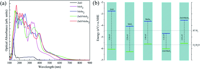 |
| | Fig. 6 (a) Calculated optical absorption curves and (b) band edge positions for ZnO, MoS2, MoSe2 monolayers, ZnO/MoS2, and ZnO/MoSe2 composites. The horizontal dotted lines indicate the energy levels of redox potentials of H+/H2 (−4.44 eV) and O2/H2O (−5.67 eV). The blue and green colors denote CBM and VBM, respectively. | |
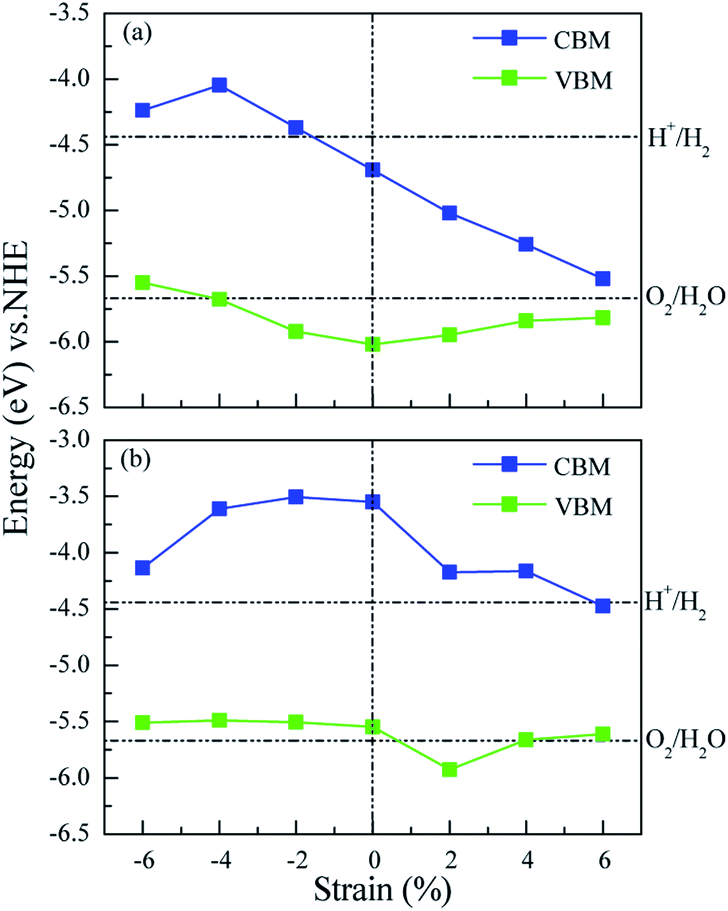
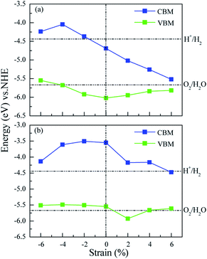
The improvement of visible light absorption may not always result in the enhancement of photocatalytic activity, and the band edge positions with respect to the water redox levels (−4.44 eV for H+ to H2 and –5.67 eV of H2O to O2)41 are important to ensure the photooxidation and photoreduction processes thermodynamically allowed. The VBM and CBM potentials of ZnO, MoS2, MoSe2 monolayers, ZnO/MoS2, and ZnO/MoSe2 composites with respect to the water reduction and oxidation potentials are shown in Fig. 6b. For ZnO and MoS2 monolayers, the VBM and CBM straddle the water oxidation and reduction potentials, which is energetically favorable for oxidation and reduction processes. While for monolayer MoSe2, the VBM is higher than the water oxidation potential, so it is thermodynamically unfavorable for oxygen production. For ZnO/MoS2 composite, the VBM is more lower than the water oxidation potential and the CBM is more lower than the hydrogen reduction potential, which is suitable for photooxidation process but not suitable for photoreduction process. This result could not give a reasonable explanation about the high hydrogen production rate of MoS2 nanosheet-ZnO heterostructure,24 which is due to the fact that the ZnO/MoS2 we studied is constructed by ZnO and MoS2 monolayers and the ZnO/MoS2 heterostructure reported by experiment is MoS2 nanosheet-coated on ZnO multilayers. For ZnO/MoSe2 composite, the VBM is more higher than the water oxidation potential and the CBM is more higher than hydrogen reduction potential, which is unfavorable for photooxidation process.
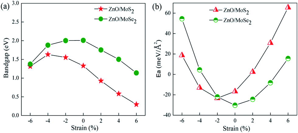
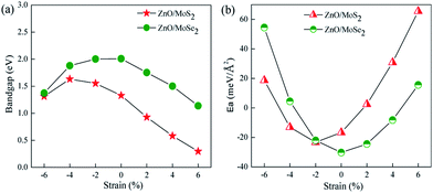
Many studies42–44 have proved that the application of strain is a useful method to adjust the band structures and band edge positions with respect to water redox levels. The biaxial strain applied in the x and y directions with the range from −6% to 6% has been adopted to tune the electronic structures of ZnO/MoS2 and ZnO/MoSe2 heterostructures, the varied bandgaps for ZnO/MoS2 and ZnO/MoSe2 composites with different strains are displayed in Fig. 7a. The bandgaps for ZnO/MoS2 composites increase with the strain from −6% to −4% and decrease with the strain from −4% to +6%. But for ZnO/MoSe2 composites, the bandgaps increase with the strain from −6% to 0 and decrease with the strain from 0 to +6%. The interface adhesion energies for ZnO/MoS2 and ZnO/MoSe2 composites with different strains are shown in Fig. 7b, the interface adhesion energies for ZnO/MoS2 composites decrease with the strain from −6% to −2% and increase with the strain from −2% to +6%. But for ZnO/MoSe2 composites, the interface adhesion energies decrease with the strain from −6% to 0 and increase with the strain from 0 to +6%. The ZnO/MoS2 composite with the strain of −2% and the ZnO/MoS2 composite without strain are energetically favorable in our considered composites. The band edge positions for ZnO/MoS2 and ZnO/MoSe2 with different biaxial strains are plotted in Fig. 8. The bandgaps for ZnO/MoS2 heterostructures applied the strain with the range from −6% to 6% are respectively 1.31, 1.63, 1.55, 1.33, 0.93, 0.58, and 0.30 eV, whereas the bandgaps for ZnO/MoSe2 heterostructures applied the strain with the range from −6% to 6% are respectively 1.37, 1.88, 2.00, 2.01, 1.75, 1.50, and 1.14 eV. It can been seen clearly that the ZnO/MoS2 heterostructure with the strain of −2% and ZnO/MoSe2 heterostructure with the strain of +2% have proper bandgaps with the band edge positions straddling the water redox levels, so it is thermodynamically favorable for water photooxidation and photoreduction processes.
 |
| | Fig. 7 (a) Varied bandgaps and (b) interface adhesion energies (Ea) for ZnO/MoS2 and ZnO/MoSe2 composites with different strains. | |
 |
| | Fig. 8 Band edge positions of (a) ZnO/MoS2 and (b) ZnO/MoSe2 composites as a function of biaxial strain as compared with the water redox potentials of H+/H2 and O2/H2O. The vertical lines represent unstrained ZnO/MoS2 or ZnO/MoSe2 composites. | |
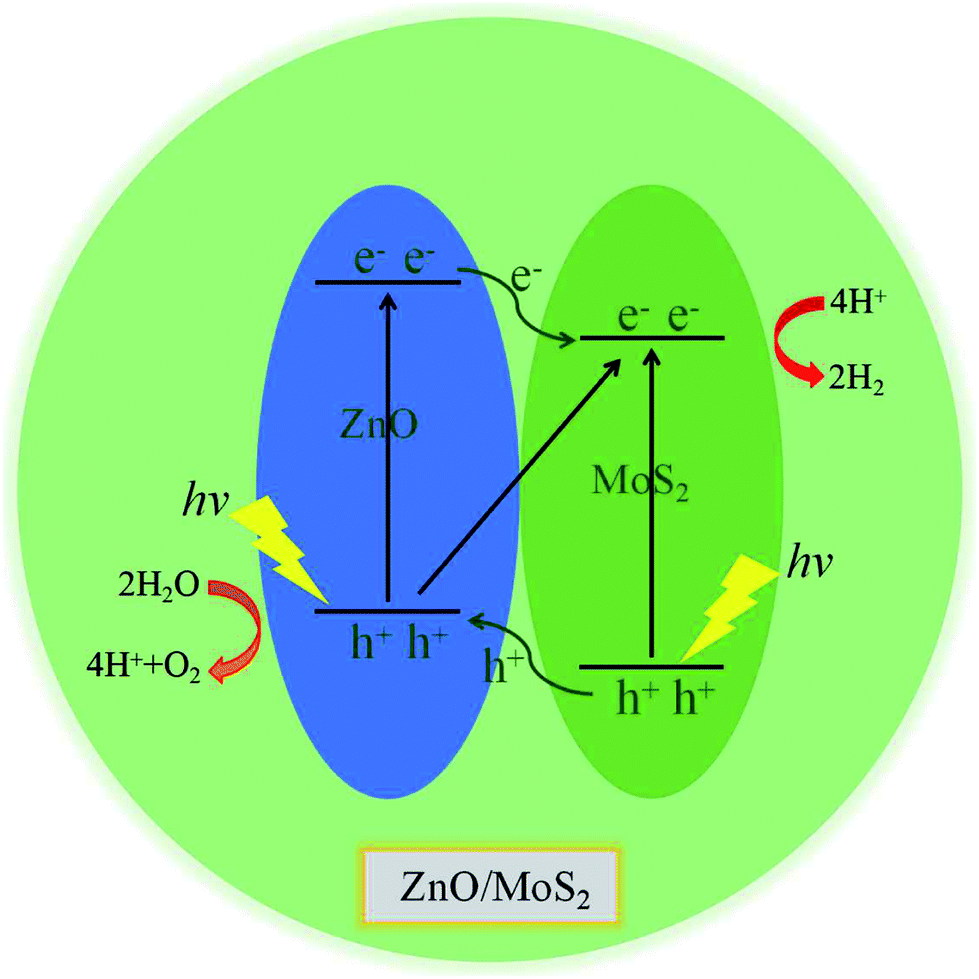
We have gives the DOS, PDOS, and band structures for ZnO/MoS2 with the strain of −2% and ZnO/MoSe2 with the strain of +2% in Fig. 9 to further understand the photocatalytic mechanism of these heterostructures. The ZnO/MoS2 with the strain of −2% is an indirect bandgap semiconductor with the VBM and CBM respectively locating on the k-point of Γ and K. The VBM is mainly comprised of Zn 3d, O 2p states, while the CBM is dominated by Mo 4d states. Considering the electronic transition of angular momentum selection rules (Δl = ±1), the electrons below the Fermi level will absorb photo energy and jump from O 2p states to Mo 4d states, suggesting the photoexcited electrons will transfer from ZnO layer to MoS2 layer. Therefore, the oxygen release mainly takes place in ZnO layer, and the hydrogen production locates at the MoS2 layer. These will be favorable for electron–hole separation and efficient photocatalysis. Fig. 10 also gives the schematic illustration of the carrier transfer and separation in the ZnO/MoS2 composite. The CBM and VBM of the ZnO layer are energetically higher than those of MoS2 layer, meaning that ZnO and MoS2 form a type-II heterostructure. Under irradiation, the electrons in valence band of both ZnO and MoS2 layers could be photoexcited. Ascribed to the conduction band offset, the photogenerated electrons in the CBM of ZnO layer can migrate fast to the VBM of MoS2 layer. Meanwhile, the valence band offset promotes the photogenerated holes to transfer from the VBM of MoS2 layer to the VBM of ZnO layer. Both the valence bans offset and conduction band offset promote the redistribution of photogenerated carriers. The ZnO/MoSe2 system with the strain of +2% has direct bandgap with VBM and CBM locating at the same k-point of K. The VBM is mainly contributed by Mo 4d and Se 4p states, whereas the CBM is dominated by Mo 4d states. Under light irradiation most electrons under the Fermi level jump from Se 4p states to Mo 4d states. The Bader analysis also suggests that electrons transfer from ZnO side to MoS2 (MoSe2) side after applying biaxial strain, which is favorable for separation of electron holes. Therefore, the photocatalytic ability of ZnO/MoS2 and ZnO/MoSe2 composites could be improved through mechanical strain.
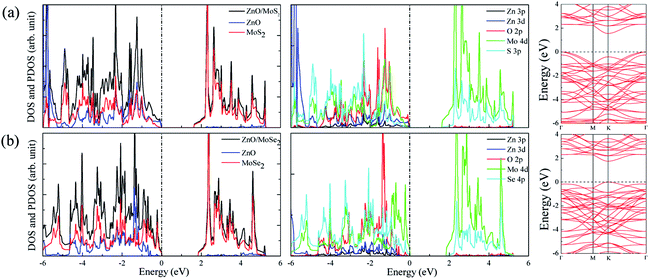 |
| | Fig. 9 DOS, PDOS, and band structures for (a) ZnO/MoS2 with the strain of −2% and (b) ZnO/MoSe2 with the strain of +2%. | |
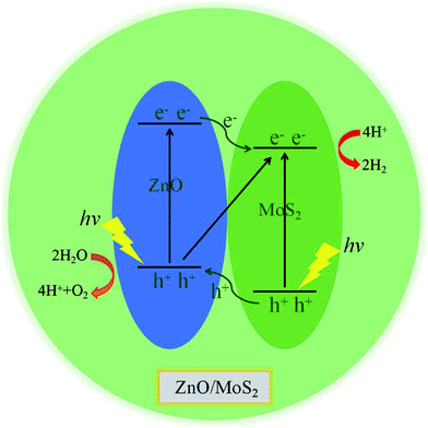 |
| | Fig. 10 Schematic illustration of the carrier transfer and separation in the ZnO/MoS2 composite. | |
4 Conclusions
In this study, the structural, electronic, and optical properties of ZnO/MoS2 and ZnO/MoSe2 composites have been investigated by utilization of hybrid density functional as compared to those of ZnO, MoS2, and MoSe2 monolayers. The ZnO/MoS2 (ZnO/MoSe2) heterostructure is easy to be synthesized because of the negative interface adhesion energies and the weak vdW interactions between the ZnO and MoS2 (MoSe2) monolayers. The charge density difference and Bader charge analysis indicate that electrons transfer from ZnO side to MoS2 (MoSe2) side, and this character will promote the efficient separation and transportation of photo-generated carriers and thus is favorable for improving the photocatalytic efficiency. Besides, the ZnO/MoS2 and ZnO/MoSe2 composites could absorb enough visible light. Through the application of strain, the ZnO/MoS2 and ZnO/MoSe2 composites could own suitable bandgap with proper VBM and CBM for visible light photocatalytic water splitting. The above findings suggest ZnO/MoS2 and ZnO/MoSe2 composites are promising photocatalysts for water splitting.
Conflicts of interest
There are no conflicts to declare.
Acknowledgements
This work was supported by the Natural Science Foundation of Chongqing under Grant No. CSTC-2011BA6004 and CSTC-2008BB4253.
References
- Q. H. Wang, K. Kalantar-Zadeh, A. Kis, J. N. Coleman and M. S. Strano, Nat. Nanotechnol., 2012, 7, 699–712 CrossRef PubMed.
- F. A. Rasmussen and K. S. Thygesen, J. Phys. Chem. C, 2015, 119, 13169–13183 CrossRef.
- T. Cheiwchanchamnangij and W. R. Lambrecht, Phys. Rev. B: Condens. Matter Mater. Phys., 2012, 85, 205302 CrossRef.
- A. B. Laursen, S. Kegnæs, S. Dahl and I. Chorkendorff, Energy Environ. Sci., 2012, 5, 5577–5591 Search PubMed.
- X. Yang, J. Li, T. Liang, C. Ma, Y. Zhang, H. Chen, N. Hanagata, H. Su and M. Xu, Nanoscale, 2014, 6, 10126–10133 RSC.
- H. Wan, L. Xu, W. Q. Huang, J. H. Zhou, C. N. He, X. Li, G. F. Huang, P. Peng and Z. G. Zhou, RSC Adv., 2015, 5, 7944–7952 RSC.
- N. Singh, G. Jabbour and U. Schwingenschlögl, Eur. Phys. J. B, 2012, 85, 1–4 CrossRef.
- G. Wang, Y. Huang, A. Kuang, H. Yuan, Y. Li and H. Chen, Inorg. Chem., 2016, 55, 9620–9631 CrossRef PubMed.
- G. Wang, H. Chen, Y. Li, A. Kuang, H. Yuan and G. Wu, Phys. Chem. Chem. Phys., 2015, 17, 28743–28753 RSC.
- Y. Qu and X. Duan, Chem. Soc. Rev., 2013, 42, 2568–2580 RSC.
- G. Z. Wang, S. Dang, P. Zhang, S. Xiao, C. Wang and M. Zhong, J. Phys. D: Appl. Phys., 2017, 51, 025109 CrossRef.
- H. Li, K. Yu, X. Lei, B. Guo, H. Fu and Z. Zhu, J. Phys. Chem. C, 2015, 119, 22681–22689 CrossRef.
- P. Wang, P. Shi, Y. Hong, X. Zhou and W. Yao, Mater. Res. Bull., 2015, 62, 24–29 CrossRef.
- B. Han and Y. H. Hu, Energy Environ. Sci., 2016, 4, 285–304 Search PubMed.
- Y. F. Zhao, Z. Y. Yang, Y. X. Zhang, L. Jing, X. Guo, Z. Ke, P. Hu, G. Wang, Y. M. Yan and K. N. Sun, J. Phys. Chem. C, 2014, 118, 14238–14245 CrossRef.
- X. Zong, H. Yan, G. Wu, G. Ma, F. Wen, L. Wang and C. Li, J. Am. Chem. C, 2008, 130, 7176–7177 CrossRef PubMed.
- Q. Xiang, J. Yu and M. Jaroniec, J. Am. Chem. C, 2012, 134, 6575–6578 CrossRef PubMed.
- J. Li, K. Yu, Y. Tan, H. Fu, Q. Zhang, W. Cong, C. Song, H. Yin and Z. Zhu, Dalton Trans., 2014, 43, 13136–13144 RSC.
- B. Weng, X. Zhang, N. Zhang, Z.-R. Tang and Y.-J. Xu, Langmuir, 2015, 31, 4314–4322 CrossRef PubMed.
- Q. Li, N. Zhang, Y. Yang, G. Wang and D. H. Ng, Langmuir, 2014, 30, 8965–8972 CrossRef PubMed.
- L. Ge, C. Han, X. Xiao and L. Guo, Int. J. Hydrogen Energy, 2013, 38, 6960–6969 CrossRef.
- K. Chang, Z. Mei, T. Wang, Q. Kang, S. Ouyang and J. Ye, ACS Nano, 2014, 8, 7078–7087 CrossRef PubMed.
- Y.-H. Tan, K. Yu, J.-Z. Li, H. Fu and Z.-Q. Zhu, J. Appl. Phys., 2014, 116, 064305 CrossRef.
- Y.-J. Yuan, F. Wang, B. Hu, H.-W. Lu, Z.-T. Yu and Z.-G. Zou, Dalton Trans., 2015, 44, 10997–11003 RSC.
- J. Lee, D. C. Sorescu and X. Deng, J. Phys. Chem. Lett., 2016, 7, 1335–1340 CrossRef PubMed.
- S. Kang, T. Wu, X. Li and J. Mu, Colloids Surf., A, 2010, 369, 268–271 CrossRef.
- T. Kaewmaraya, A. De Sarkar, B. Sa, Z. Sun and R. Ahuja, Comput. Mater. Sci., 2014, 91, 38–42 CrossRef.
- J. P. Perdew, K. Burke and M. Ernzerhof, Phys. Rev. Lett., 1996, 77, 3865 CrossRef PubMed.
- M. Ernzerhof and G. E. Scuseria, J. Chem. Phys., 1999, 110, 5029–5036 CrossRef.
- G. Kresse and J. Furthmüller, Phys. Rev. B: Condens. Matter Mater. Phys., 1996, 54, 11169 CrossRef.
- P. E. Blöchl, Phys. Rev. B: Condens. Matter Mater. Phys., 1994, 50, 17953 CrossRef.
- S. Grimme, J. Antony, S. Ehrlich and H. Krieg, J. Chem. Phys., 2010, 132, 154104 CrossRef PubMed.
- J. Heyd, G. E. Scuseria and M. Ernzerhof, J. Chem. Phys., 2003, 118, 8207–8215 CrossRef.
- J. Heyd, G. E. Scuseria and M. Ernzerhof, J. Chem. Phys., 2006, 124, 219906 CrossRef.
- S. Saha, T. Sinha and A. Mookerjee, Phys. Rev. B: Condens. Matter Mater. Phys., 2000, 62, 8828 CrossRef.
- H. Guo, Y. Zhao, N. Lu, E. Kan, X. C. Zeng, X. Wu and J. Yang, J. Phys. Chem. C, 2012, 116, 11336–11342 CrossRef.
- H.-P. Komsa and A. V. Krasheninnikov, Phys. Rev. B: Condens. Matter Mater. Phys., 2015, 91, 125304 CrossRef.
- J. Kang, S. Tongay, J. Zhou, J. Li and J. Wu, Appl. Phys. Lett., 2013, 102, 012111 CrossRef.
- J. Liao, B. Sa, J. Zhou, R. Ahuja and Z. Sun, J. Phys. Chem. C, 2014, 118, 17594–17599 CrossRef.
- T. BjöRkman, A. Gulans, A. V. Krasheninnikov and R. M. Nieminen, Phys. Rev. Lett., 2012, 108, 1577–1581 CrossRef PubMed.
- X. Li, J. Zhao and J. Yang, Sci. Rep., 2013, 3, 1858 CrossRef PubMed.
- J. Feng, X. Qian, C. W. Huang and J. Li, Nat. Photonics, 2012, 6, 865–871 CrossRef.
- N. Lu, H. Guo, L. Li, J. Dai, L. Wang, W. N. Mei, X. Wu and X. C. Zeng, Nanoscale, 2013, 6, 2879–2886 RSC.
- W. S. Yun, S. W. Han, S. C. Hong, I. G. Kim and J. D. Lee, Phys. Rev. B: Condens. Matter Mater. Phys., 2012, 85, 033305 CrossRef.
|
| This journal is © The Royal Society of Chemistry 2018 |
Click here to see how this site uses Cookies. View our privacy policy here. 
 Open Access Article
 This Open Access Article is licensed under a Creative Commons Attribution-Non Commercial 3.0 Unported Licence
 a,
Junli Changa,
Biao Wanga,
Anlong Kuanga and
Hong Chen
a,
Junli Changa,
Biao Wanga,
Anlong Kuanga and
Hong Chen