
High-performance organic field-effect transistors based on organic single crystal microribbons fabricated by an in situ annealing method†
Ji
Zhang‡
a,
Zhaoguang
Li‡
b,
Weifeng
Zhang
a,
Man Shing
Wong
 *b and
Gui
Yu
*ac
*b and
Gui
Yu
*ac
aCAS Key Laboratory of Organic Solids, CAS Research/Education Center for Excellence in Molecular Sciences, Institute of Chemistry, Chinese Academy of Sciences, Beijing 100190, P. R. China. E-mail: yugui@iccas.ac.cn
bInstitute of Molecular Functional Materials, Department of Chemistry, and Institute of Advanced Materials, Hong Kong Baptist University, Kowloon Tong, Hong Kong SAR, P. R. China. E-mail: mswong@hkbu.edu.hk
cSchool of Chemical Sciences, University of Chinese Academy of Sciences, Beijing 100049, P. R. China
First published on 4th September 2018
Abstract
In situ fabrication of microribbon transistors has been considered an efficient and facile approach compared with normal solution method or physical vapor transport techniques, and could also prevent the introduction of impurities. Herein, the naphtho[2,1-b:3,4-b′]bisthieno[3,2-b][1]benzothiophene derivative (NBTBT-6) with two alkoxy-side chains was used to fabricate single crystal microribbon-based transistors by in situ annealing of the NBTBT-6 thin films. Carrier mobilities of transistors based on the NBTBT-6 microribbons were one order of magnitude higher than those of thin film devices. Related characterizations of the NBTBT-6 microribbon showed its single crystalline structure with good directionality. Furthermore, the process of crystal formation is discussed.
Introduction
Since the fabrication of the first organic field-effect transistor (OFET),1 30 years have passed, and there has been tremendous progress in both areas of organic/polymer semiconducting materials and devices.2–6 Numerous organic semiconductors with film mobility exceeding 1 cm2 V−1 s−1 have been synthesized. However, the microstructures of amorphous films deposited by vapor-evaporation or solution method can easily trap and scatter charge carriers, resulting in relatively poor performance. Therefore, the enhancement of molecular packing order in semiconductors is considered an effective way to optimize the charge carrier mobility.7,8Single crystal formation has proven to be an appropriate solution to avoid massive disorders in the organic layer.9,10 As an example, the charge carrier mobility of single crystal pentacene is about 40 cm2 V−1 s−1, which is one order of magnitude higher than that of the vapor-evaporated pentacene film with mobility of up to 6.5 cm2 V−1 s−1.11 Additionally, with a microribbon-shape semiconductor, the single-crystal device may be smaller and easy to integrate while the consumption of the semiconductor materials is reduced, thus making microribbons a hot area of research and a promising candidate for future applications.12,13 There are numerous research studies on organic single-crystal microribbon transistors, focusing on the preparation of high quality crystals,14,15 the detailed study of the charge transport mechanism16 and the applications including sensors,17–19 optical switch devices20 and several microstructure-induced techniques.21
Nowadays, the physical vapor transport (PVT) technique is considered the best way to obtain high-quality single crystals with the least number of defects and highest order. Moreover, the conditions of evaporation are easy to control in order to get a different shape and size of single crystal. However, the PVT technique with its cumbersome process relies on an expensive vacuum instrument. In addition, the organic materials should be stable enough to be evaporated and recrystallized, which restricts the application of polymers and unstable small molecules. The solution-process method is another widely used way to obtain high-quality microribbon crystal.22,23 For example, the first solution-processed OFET device with mobility exceeding 1 cm2 V−1 s−1 was fabricated based on microribbons of tetrathiafulvalene derivatives by Torrent et al.24 Nevertheless, the solution process also faces adverse conditions, sometimes. The materials should show good solubility and easily precipitate and the as-prepared crystal should be transferable to the substrate. However, contamination and breakage of crystal samples of organic semiconductors often occurs on employing the solution process. Moreover, it is difficult to obtain high-quality single crystals by the in situ direct-growth solution process method.
In this study, we developed an in situ method to fabricate high mobility organic microribbon transistors via annealing of a thin film sample. A 2 nm ultra-thin layer was first deposited by spin-coating or vacumm-evaporation based on NBTBT-6 that has been reported in our previous study.25 Then, annealing at 230 °C was performed to facilitate the self-assembling of NBTBT-6 molecules and the formation of single-crystal microribbons. Due to the better molecular packing order, which was proved by detailed characterizations, carrier mobilities of transistors based on single crystal microribbons of NBTBT-6 were one order of magnitude higher than those of thin film devices. At last, the formation process of microribbons is discussed based on atomic force microscopy (AFM) images.
Results and discussion
The molecular structure of the organic semiconductor NBTBT-6 is shown in Fig. 1. The NBTBT-6 molecule contains two alkoxy-side chains, which have more degrees of freedom to rotate compared with normal alkyl-side chains, which are crucial to the morphology and crystallinity transformation of thin films at higher temperatures.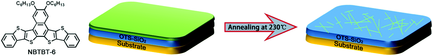 | ||
| Fig. 1 Molecular structure of organic semiconductor NBTBT-6 and in situ annealing of the NBTBT-6 thin films to fabricate the microribbons. | ||
Differential scanning calorimetry (DSC) measurements were performed and the heat flow as a function of the temperature is shown in Fig. 2a. Generally, the two endothermic peaks at 154.4 and 249.1 °C indicate the movement of the long side-chains and the melting point, respectively. In Fig. S1 (ESI†), AFM images of 35 nm NBTBT-6 film after annealing at different temperatures reveal that the thin film tends to be more well-organized with higher annealing temperature. Compared with amorphous films obtained below 160 °C, small crystalline grains begin to form over 160 °C, and the grains become larger and higher in order until 240 °C. Then, the film will melt over 240 °C, which is consistent with the variation trend of charge carrier mobility of an organic thin film transistor (OTFT). As shown in Fig. 2b, the mobility as a function of the annealing temperature increases at temperatures over 120 °C. In order to better investigate the variation trend of crystallinity of the thin film, both out-of-plane and in-plane XRD were performed (Fig. S2, ESI†). The strongest diffraction patterns appear after annealing at a temperature of around 230–240 °C, which is also in accordance with the carrier mobility results.
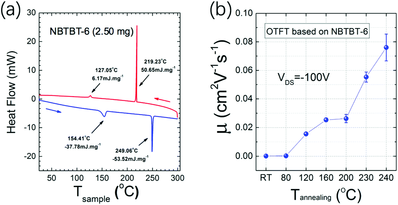 | ||
| Fig. 2 (a) Differential scanning calorimetry (DSC) of NBTBT-6 powder and (b) μFET of organic thin film transistor in the saturation regimes as a function of the annealing temperature of NBTBT-6 film. | ||
It is noteworthy that the RMS roughness of the film after annealing at different temperatures does not change significantly from room temperature (RT) to 240 °C (Fig. S1, ESI†), but the morphology of the film is totally different, suggesting the formation of a ribbon-like structure at the dielectric–organic interface, which may induce the upper layers to show rectilinear boundaries. To better understand the morphology, an experiment similar to molecular beam epitaxy was performed to graphically mark the orientation of the microstructure in the thin film. As shown in Fig. S3b (ESI†), the 35 nm NBTBT-6 film was first annealed at 240 °C, followed by vapor-deposition of the 2 nm NBTBT-6 thin film. Compared with the as-prepared film, the 2 nm layer shows the clear grain orientations and rectilinear boundaries. This is an interesting experimental phenomenon that substantiates the possibility to fabricate high-quality microribbons.
To find the best annealing conditions, 2 nm NBTBT-6 film was annealed at different temperatures successively from RT to 240 °C. As shown in Fig. S4 (ESI†), 230 °C was found to be the critical annealing temperature to form microribbons. The octadecyltrichlorosilane (OTS)-modified surface is also a key to help form microribbons instead of irregular shapes on a pure SiO2 surface (shown in Fig. S5, ESI†). By controlling the experimental conditions, microribbons with different sizes and shapes were prepared (Fig. 3a–c). Their morphology depends strongly on the annealing temperature (Fig. S4, ESI†); high-performance transistors based on high-quality single crystal microribbons can be easily fabricated by manual pasting a gold source and draining electrodes directly on the microribbon under a microscope (Fig. 4a). The microribbon-based transistors exhibit typical hole transport properties with the highest mobility of 0.94 cm2 V−1 s−1 and an ON/OFF current ratio exceeding 107 (Fig. 4b and c). OTFTs-based NBTBT-6 thin films, in contrast, exhibit an average mobility up to 0.078 cm2 V−1 s−1 with an ON/OFF current ratio of about 106 (Fig. S6, ESI†).
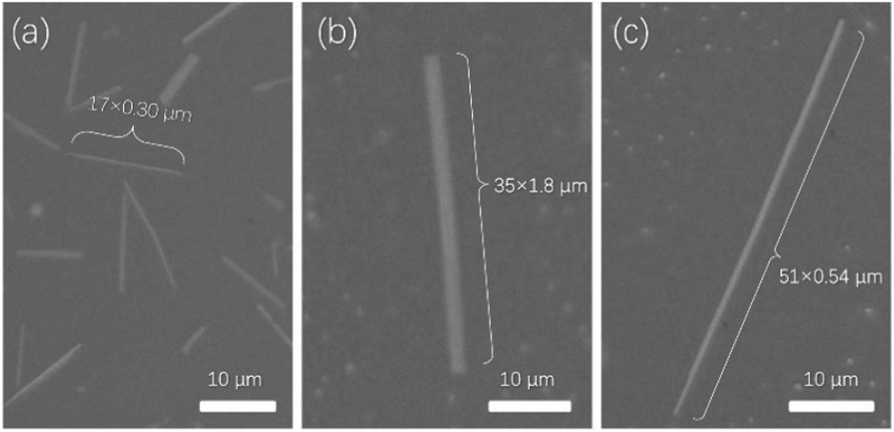 | ||
| Fig. 3 Different microphotographs of microribbons: (a) 17 μm × 0.30 μm (b) 35 μm × 1.8 μm (c) 51 μm × 0.54 μm. | ||
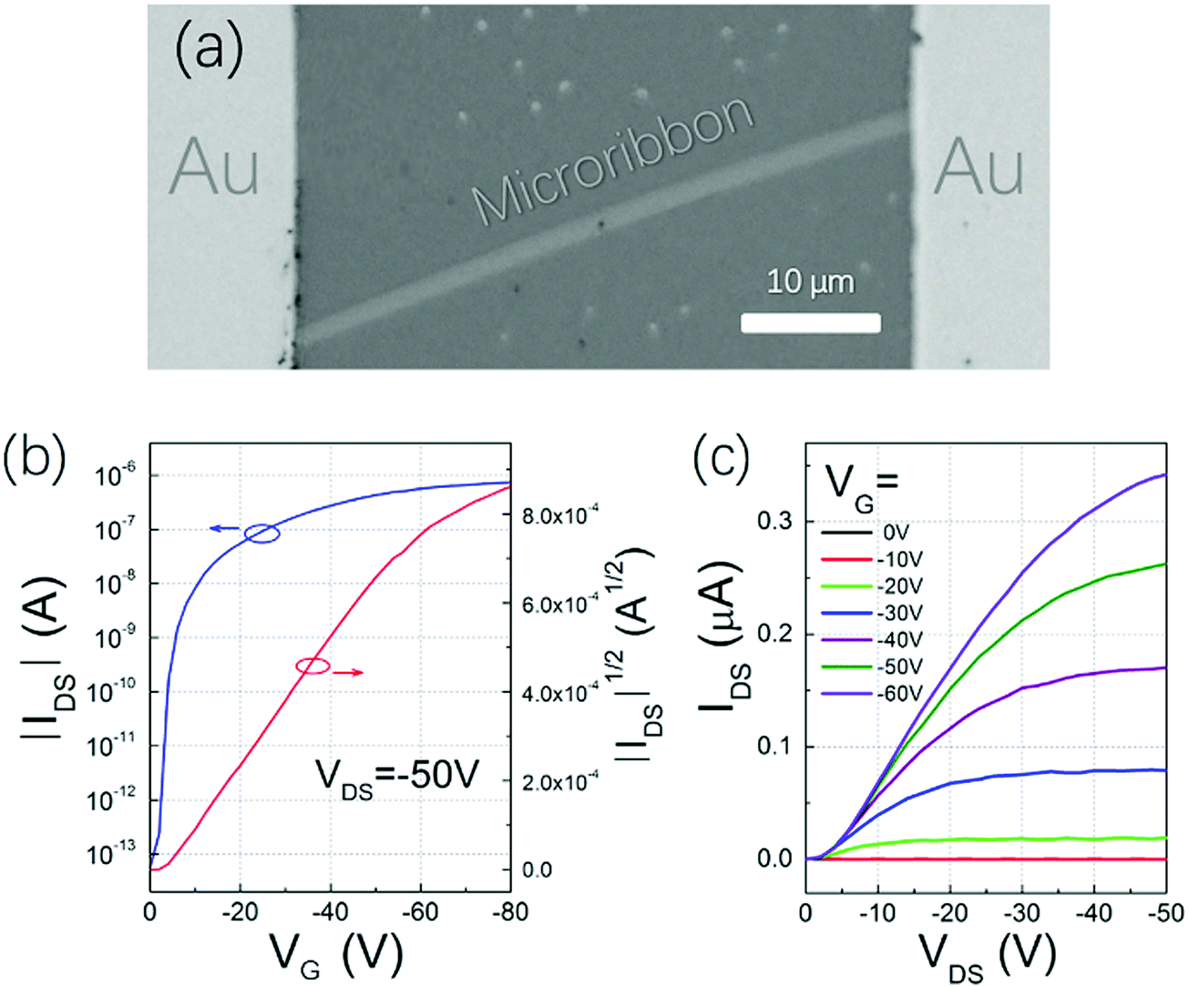 | ||
| Fig. 4 (a) Microphotograph and typical (b) transfer and (c) output characteristics of NBTBT-6 microribbon-based transistors. | ||
High resolution transmission electron microscopy (HRTEM), selected area electron diffraction (SAED) and scanning electron microscopy (SEM) were performed to analyze the crystallinity and morphology of the microribbon. HRTEM shows the crystal lattice orientation indicated by the white arrows in the image in Fig. 5d, and the lattice distance was calculated to be 2.71 Å. A fast Fourier transform (FFT) image with several clear patterns is shown in Fig. 5a. SAED diffraction patterns shown in Fig. 5b demonstrate the single crystal character of the NBTBT-6 microribbon. In addition, the SEM image visually shows that the microribbon reveals sharp edges with good orientation. To better investigate the annealing process of the micro-ribbon, out-of-plane X-ray diffraction (XRD) was performed with different annealing times. The 2 nm thin film was annealed at 230 °C successively for 1, 5 and 60 min. The XRD results are shown in Fig. 6b; with the increase in annealing time, out-of-plane diffractions have a tendency to be stronger with two peaks at ∼3.50°, corresponding to dspacing = 25.5 Å. It is clear that the peak positions do not change upon annealing, which indicates that the diffraction signal strengthens in the direction of (001) without any phase transition in the microribbon, suggesting that there are more layers in the direction perpendicular to the substrate.
 | ||
| Fig. 5 (a) Fast Fourier transform (FFT) of select area of high resolution HRTEM image. (b) SAED pattern (c) SEM image and (d) HRTEM image. | ||
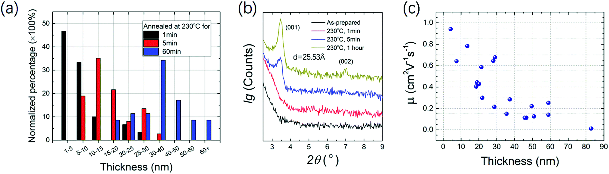 | ||
| Fig. 6 (a) Normalized percentage as a function of microribbon thickness with different annealing time (more than 30 microribbons are measured at each condition) (b) out-of-plane XRD patterns with different annealing time (c) μFET distribution as a function of the thickness of NBTBT-6 microribbons. | ||
In Fig. 6a, normalized percentage as a function of microribbon thickness with different annealing time is shown, which clearly reveals that the microribbons tend to become thicker with the increase in annealing time. More than 30 microribbons were measured and summarized to show the statistical data. The mode values for 1, 5, and 60 min are 1–5, 10–15 and 30–40 nm, respectively, which is consistent with the XRD variation trends. A simple thermodynamics principle could be applied to explain this trend. On the very low surface energy OTS-microribbon interface, organic molecules with larger surface energy tend to aggregate to decrease the surface area. With the increase in annealing time, the microribbon will be thicker. Mobility distribution as a function of the microribbon thickness is measured and shown in Fig. 6c. The mobility tends to decrease as the ribbons become thicker, which may because the thicker microribbon contains more defects at the edges and a long-time annealing process will significantly decrease the surface area, resulting in poor continuity along the growth direction. This result is consistent with several reports.26–28
To better investigate the origin of the morphology of the microribbon, AFM was performed, and different scale images are shown in Fig. 7. According to these AFM images, the microribbons show excellent crystallinity in the growth direction. AFM images in Fig. 7c and d show a nearly rectilinear boundary on the surface of the microribbon, which is clearly shown from the section view of the height image in Fig. 7i, in which an altitude difference was estimated to be 1.53 nm with the total height of the microribbon about 13.7 nm. The altitude difference of 1.53 nm is approximately equal to a single molecule length of 1.57 nm, which is clearly smaller than the dspacing of 2.55 nm calculated from the XRD patterns, as discussed in the previous section. This difference indicates that the top layer on the microribbon is not the periodical unit layer, and needs additional molecules to form a periodical structure.
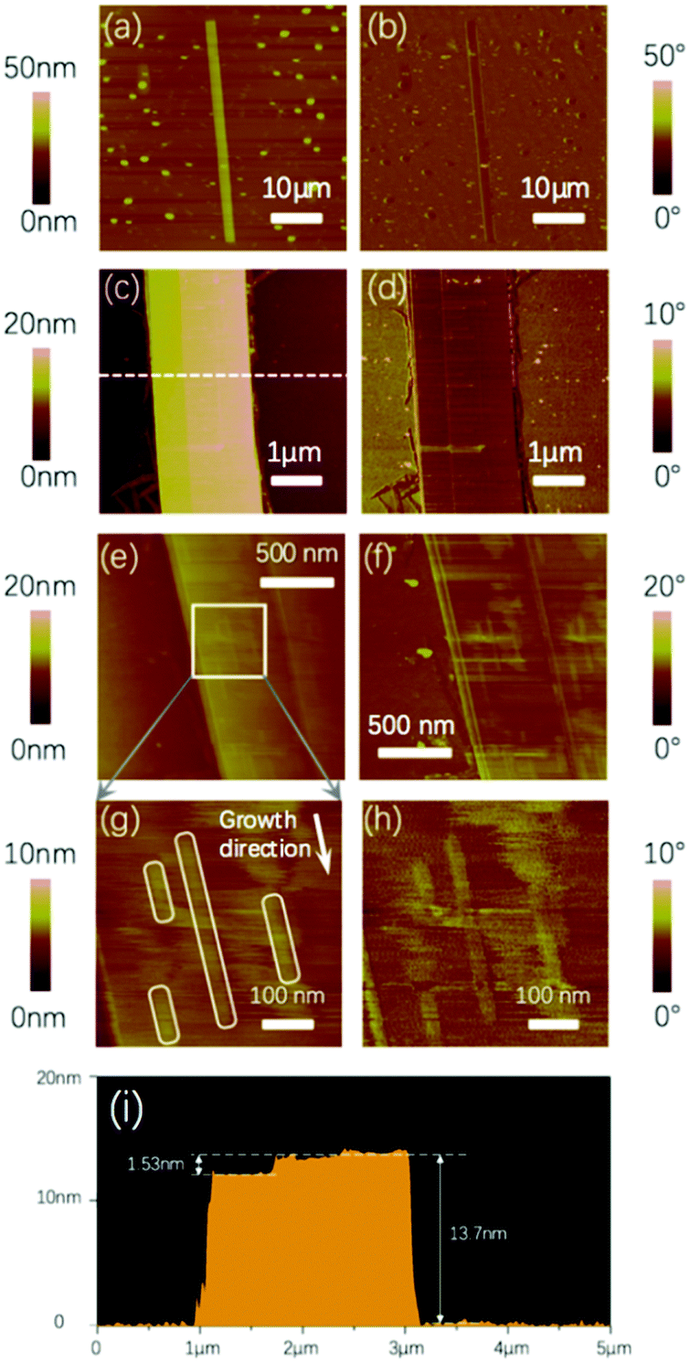 | ||
| Fig. 7 AFM height and phase images of microribbons in different scales: (a) and (b) 50 μm; (c) and (d) 5 μm; (e) and (f) 1.7 μm; (g) and (h) 500 nm (b), (d), (f) and (h) are the phase images corresponding to the left height images. (i) The section view indicated by the white dashed line in (c). | ||
As shown in Fig. 7g and h, there are numerous nanoribbon-like structures on the surface, which exhibit a width of 25–30 nm. These nanostructures and the rectilinear boundaries on the microribbon demonstrate a model of a formation process at thermodynamic equilibrium. NBTBT-6 molecules aggregate to form a single crystal microribbon with Frank–van der Merwe growth mode, which is shown clearly in the AFM images. The formation of the rectilinear boundary is due to the lack of an external molecule supplement, and the relatively high temperature stimulates the molecule to overwhelm the energy barrier to form a crystal lattice when the temperature returns to RT. Additionally, to verify that the layer-by-layer growth mode is ubiquitous in most microribbons, two typical microphotographs are shown in Fig. S6 (ESI†), which is similar to the microribbon illustrated in Fig. 7c.
Conclusions
In summary, we developed an in situ method to fabricate high-mobility organic microribbons via annealing of the thin film simple. Carrier mobilities of the transistors based on single crystal microribbons were one order of magnitude higher than those of thin film devices with high ON/OFF current ratio exceeding 107. Systematic characterizations were performed and it was shown that the microribbons exhibited a single crystalline structure. The molecules were rapidly evaporated or solution-processed on the OTS-SiO2/Si substrate, and tend to form a loosely packed structure because of the weak intermolecular forces and high molecular deformability. The nonuniformity and surface potential barrier will hinder the formation of a perfect crystalline layer. At higher annealing temperature, the molecules with enough energy will occupy the barrier position on the substrate. Consequently, the thin film turns into a neat and tight layer dominated by the intermolecular forces. In addition, the morphology of these microribbons could also be controlled by modifying the dielectric surface, which implies a simple way to pattern the microribbons. This method with no need of transference seems to be a promising approach to obtain crystalline transistors for future applications.Experimental section
Materials and methods
Electronic properties of the OFETs devices were measured using Keithley 4200SCS semiconductor parameter analyser in air. The X-ray diffraction (XRD) measurements were performed using D/max 2500 X-Ray Diffractometer, with scan rate at 3–5° min−1. The atomic force microscopy (AFM) measurements were performed on Veeco Nanoscope IV under tapping mode. The scanning electron microscopy (SEM) images were recorded on Hitachi S-4800. The transmission electron microscopy (TEM) images were recorded using JEOL JEM-2011. The microscope used was Olympus, BX51 + DP27. Differential scanning calorimetry (DSC) was performed using DSC822e.Fabrication of OTFT devices
OTFT devices were fabricated in a bottom-gate bottom-contact (BGBC) configuration (gold electrode on Si/SiO2 substrates). Octadecyltrichlorosilane (OTS) treatment was performed on the gate dielectrics that were placed in a vacuum oven with OTS at a temperature of 120 °C for 3 h to form an OTS self-assembled monolayer. This was followed by cleaning of the substrate and deposition of organic semiconductors by vacuum-evaporation at the rate of 6–10 Å min−1. The film thickness of the organic semiconductor layer was controlled by a quartz crystal microbalance monitor. Mobility of the devices was calculated in the saturation regime. The equation used was as follows:| IDS = (W/2L)Ciμ(VGS − Vth)2 |
Fabrication of microribbon devices
Microribbon transistors were fabricated in a bottom-gate top-contact (BGBC) configuration (gold electrodes transferred onto organic microribbon). Octadecyltrichlorosilane (OTS) treatment was performed on the gate dielectrics that were placed in a vacuum oven with OTS at a temperature of 120 °C for 3 h to form an OTS self-assembled monolayer. This was followed by cleaning of the substrate and deposition of organic semiconductors by vacuum-evaporation at the rate of 1–2 Å min−1. The film thickness was controlled by a quartz crystal microbalance monitor. Mobility of the devices was calculated in the saturation regime. The equation is the same as mentioned above, where W/L was the channel width/length, which was confirmed under microscopy, Ci was the insulator capacitance per unit area, and VGS and Vth were the gate voltage and threshold voltage, respectively.Conflicts of interest
The authors declare no conflict of interest.Acknowledgements
This study was financially supported by the National Key Research and Development Program of China (2017YFA0204703), National Key R&D Program of “Strategic Advanced Electronic Materials” (2016YFB0401100), and the Strategic Priority Research Program of the Chinese Academy of Sciences (CAS) (Grant No. XDB12030100). This work was also supported by a grant from the University Grants Committee, Areas of Excellence Scheme (AoE/P-03/08). The GIXRD measurements were performed at the BL14B1 Station of Shanghai Synchrotron Radiation Facility (SSRF).Notes and references
- H. Tsumura, H. Koezuka and T. Ando, Appl. Phys. Lett., 1986, 18, 1210 CrossRef.
- H. Sirringhaus, Adv. Mater., 2014, 9, 1319 CrossRef PubMed.
- K. L. Shi, W. F. Zhang, D. Gao, S. Y. Zhang, Z. Z. Lin, Y. Zou, L. P. Wang and G. Yu, Adv. Mater., 2018, 30, 1705286 CrossRef PubMed.
- J. Y. Huang, Z. P. Mao, Z. H. Chen, D. Gao, C. Y. Wei, W. F. Zhang and G. Yu, Chem. Mater., 2016, 28, 2209 CrossRef.
- Y. Q. Shi, H. Guo, M. C. Qin, J. Y. Zhao, Y. X. Wang, H. Wang, Y. L. Wang, A. Facchetti, X. H. Lu and X. G. Guo, Adv. Mater., 2018, 30, 1705745 CrossRef PubMed.
- C. Wang, X. C. Ren, C. H. Xu, B. B. Fu, R. H. Wang, X. T. Zhang, R. J. Li, H. X. Li, H. L. Dong and Y. G. Zhen, Adv. Mater., 2018, 30, 1706260 CrossRef PubMed.
- V. Coropceanu, J. Cornil, D. A. da Silva, Y. Olivier, R. Silbey and J. L. Bredas, Chem. Rev., 2007, 4, 926 CrossRef PubMed.
- A. Saeki, Y. Koizumi, T. Aida and S. Seki, Acc. Chem. Res., 2012, 8, 1193 CrossRef PubMed.
- X. J. Zhang, X. H. Zhang, K. Zou, C. S. Lee and S. T. Lee, J. Am. Chem. Soc., 2007, 129, 3527 CrossRef PubMed.
- X. J. Zhang, X. H. Zhang, W. S. Shi, X. M. Meng, C. S. Lee and S. T. Lee, Angew. Chem., Int. Ed., 2007, 119, 1547 CrossRef.
- J. E. Anthony, Chem. Rev., 2006, 12, 5028 CrossRef PubMed.
- Z. L. Wang, R. R. Bao, X. J. Zhang, X. M. Ou, C. S. Lee, J. C. Chang and X. H. Zhang, Angew. Chem., Int. Ed., 2011, 50, 2811 CrossRef PubMed.
- W. Deng, X. J. Zhang, L. Wang, J. C. Wang, Q. X. Shang, X. H. Zhang, L. M. Huang and J. S. Jie, Adv. Mater., 2015, 27, 7305 CrossRef PubMed.
- K. Kim, Y. Rho, Y. Kim, S. H. Kim, S. G. Hahm and C. E. Park, Adv. Mater., 2016, 28, 3209 CrossRef PubMed.
- H. Jiang, P. Hu, J. Ye, A. Chaturvedi, K. K. Zhang, Y. X. Li, Y. Long, D. Fichou, C. Kloc and W. P. Hu, Angew. Chem., Int. Ed., 2018, 57, 1 CrossRef.
- Z. P. Zhang, L. Jiang, C. L. Cheng, Y. G. Zhen, G. Y. Zhao, H. Geng, Y. P. Yi, L. Q. Li, H. L. Dong, Z. G. Shuai and W. P. Hu, Angew. Chem., Int. Ed., 2016, 55, 5206 CrossRef PubMed.
- Z. Y. Ji, H. L. Dong, M. Liu and W. P. Hu, Nano Res., 2009, 11, 857 CrossRef.
- G. Y. Zhao, H. L. Dong, L. Jiang, H. P. Zhao, X. Qin and W. P. Hu, Appl. Phys. Lett., 2012, 10, 103302 CrossRef.
- X. T. Zhang, Y. D. He, R. J. Li, H. L. Dong and W. P. Hu, Adv. Mater., 2016, 28, 3755 CrossRef PubMed.
- Q. H. Cui, Y. Y. Hu, C. Zhou, F. Teng, J. F. Huang, A. Zhugayevych, S. Tretiak, T. Q. Nguyen and G. C. Bazan, Adv. Funct. Mater., 2018, 28, 1702073 CrossRef.
- L. Jiang, X. Yao, H. X. Li, Y. Y. Fu, L. Chen, Q. Meng, W. P. Hu and L. Jiang, Adv. Mater., 2010, 3, 376 CrossRef PubMed.
- M. Yilmaz, M. Ozdemir, H. Erdogan, U. Tamer, U. Sen, A. Facchetti, H. Usta and G. Demirel, Adv. Funct. Mater., 2015, 35, 5669 CrossRef.
- G. De Luca, A. Liscio, P. Maccagnani, F. Nolde, V. Palermo, K. Muellen and P. Samori, Adv. Funct. Mater., 2007, 18, 3791 CrossRef.
- M. Mas-Torrent, M. Durkut, P. Hadley, X. Ribas and C. Rovira, J. Am. Chem. Soc., 2004, 4, 984 CrossRef PubMed.
- Z. Li, J. Zhang, K. Zhang, W. Zhang, L. Guo, J. Huang, G. Yu and M. S. Wong, J. Mater. Chem. C, 2015, 31, 8024 RSC.
- Y. J. Zhang, H. L. Dong, Q. X. Tang, Y. D. He and W. P. Hu, J. Mater. Chem., 2010, 33, 7029 RSC.
- H. Jiang, K. J. Tan, K. K. Zhang, X. Chen and C. Kloc, J. Mater. Chem., 2011, 13, 4771 RSC.
- C. Wang, H. Dong, L. Jiang and W. Hu, Chem. Soc. Rev., 2011, 47, 422 RSC.
Footnotes |
| † Electronic supplementary information (ESI) available. See DOI: 10.1039/c8qm00385h |
| ‡ These authors contributed equally to this work. |
| This journal is © the Partner Organisations 2018 |