
Enhancement of intra- and inter-molecular π-conjugated effects for a non-fullerene acceptor to achieve high-efficiency organic solar cells with an extended photoresponse range and optimized morphology†
Ning
Wang‡
a,
Lingling
Zhan‡
a,
Shuixing
Li
a,
Minmin
Shi
 *a,
Tsz-Ki
Lau
b,
Xinhui
Lu
b,
Rafi
Shikler
c,
Chang-Zhi
Li
a and
Hongzheng
Chen
*a
*a,
Tsz-Ki
Lau
b,
Xinhui
Lu
b,
Rafi
Shikler
c,
Chang-Zhi
Li
a and
Hongzheng
Chen
*a
aMOE Key Laboratory of Macromolecular Synthesis and Functionalization, State Key Laboratory of Silicon Materials, Department of Polymer Science and Engineering, Zhejiang University, Hangzhou 310027, P. R. China. E-mail: minminshi@zju.edu.cn; hzchen@zju.edu.cn
bDepartment of Physics, Chinese University of Hong Kong, New Territories, Hong Kong, P. R. China
cDepartment of Electrical and Computer Engineering, Ben-Gurion University of the Negev, Beer-Sheva 8410501, Israel
First published on 29th August 2018
Abstract
In this work, a new A–D–A type non-fullerene electron acceptor, DF-PCNC, which possesses an electron-donating (D) core constructed by linking a 2,5-difluorobenzene ring with two cyclopentadithiophene moieties and two electron-accepting (A) end-groups of 2-(3-oxo-2,3-dihydro-1H-cyclopenta[b]naphthalen-1-ylidene)malononitrile (NC), is designed and synthesized. Because of the extension of the π-conjugation system, DF-PCNC shows stronger and more red-shifted absorption peaks while compared to those of its counterpart, DF-PCIC, which has the same D core but smaller A terminals of 2-(3-oxo-2,3-dihydro-1H-inden-1-ylidene)malononitrile (IC). Furthermore, NC groups can enhance the intermolecular π–π stacking of DF-PCNC in the condensed state. Thus, when it is blended with a polymer donor, PBDB-T, to fabricate organic solar cells (OSCs), good morphologies of the blended films are achieved through appropriate optimizations: both donor and acceptor form highly crystalline phase-separation domains with appropriate nanoscaled sizes, which is beneficial to charge generation and transport in OSCs. As a result, the short-circuit current density (JSC) of the PBDB-T:DF-PCNC device is increased by 16% compared with that of the PBDB-T:DF-PCIC one, and a high fill factor (FF) of 72.62% is maintained, leading to a better power conversion efficiency (PCE) of 11.63%, which is the highest value for OSCs based on non-fullerene acceptors adopting decreased fused-ring D cores to date.
1. Introduction
In recent years, non-fullerene acceptors have drawn a lot of attention due to their advantages superior to traditional fullerene acceptors, such as strong light absorptions, easily tunable energy levels and good morphological stability.1,2 Benefiting from the rapid development of non-fullerene acceptors, state-of-the-art fullerene-free organic solar cells (OSCs) have surpassed their fullerene-based counterparts, giving a maximum power conversion efficiency (PCE) of over 14%.3,4Until now, the most successful architecture for non-fullerene acceptors has been an A–D–A structure,5–9 in which A represents electron-accepting end-groups, like 2-(3-oxo-2,3-dihydro-1H-inden-1-ylidene)malononitrile (IC) and rhodamine,10–12 and D is an electron-donating core, e.g. indacenodithiophene (IDT) or indacenodithieno[3,2-b]thiophene (IDTT).13–16 In such a molecular configuration, A terminals are exposed to form intermolecular π–π stacking for efficient electron transport.17 As for the D core, it is generally an all-fused ring. The fused-ring guarantees the planarity of the molecular skeleton, which is beneficial to the intramolecular charge transfer (ICT) from D to A, resulting in intense absorptions in the near-infrared range.12,16 Furthermore, the bulky side chains attached to the sp3 carbon atoms in the fused-ring core are tilted to the π-conjugated backbone, thereby, avoiding the formation of large phase-separation domains in a blended film having a donor and acceptor, which is in favor of exciton dissociation.18–21 Therefore, A–D–A type non-fullerene acceptors grant both efficient charge generation and charge transportation for fullerene-free OSCs, leading to high PCEs.
Then, a question arises: is the all-fused ring core necessary for A–D–A type non-fullerene acceptors? To answer this question, we previously reported a non-fullerene acceptor with a decreased fused-ring core, DF-PCIC.22 As shown in Scheme 1a, DF-PCIC incorporates IC as A end-groups and a special D core containing one 2,5-difluorobenzene (DFB) ring attached to a cyclopentadithiophene (CPDT) moiety on each side. The F⋯H noncovalent interaction between F atoms on the DFB unit and H atoms on the adjacent CPDT moieties can lock the molecular conformation to obtain a nearly planar geometry similar to A–D–A acceptors with all-fused ring cores.23,24 While DF-PCIC is paired with a widely used polymer donor, PBDB-T, to prepare OSCs, the resultant devices yield the best PCE of 10.14%, with an open-circuit voltage (VOC) of 0.91 V, a short-circuit current density (JSC) of 15.66 mA cm−2 and a high fill factor (FF) of 72%. This original research suggests that the connection of smaller building blocks via intramolecular noncovalent interactions is a feasible route to high-performance non-fullerene acceptors too.25–29
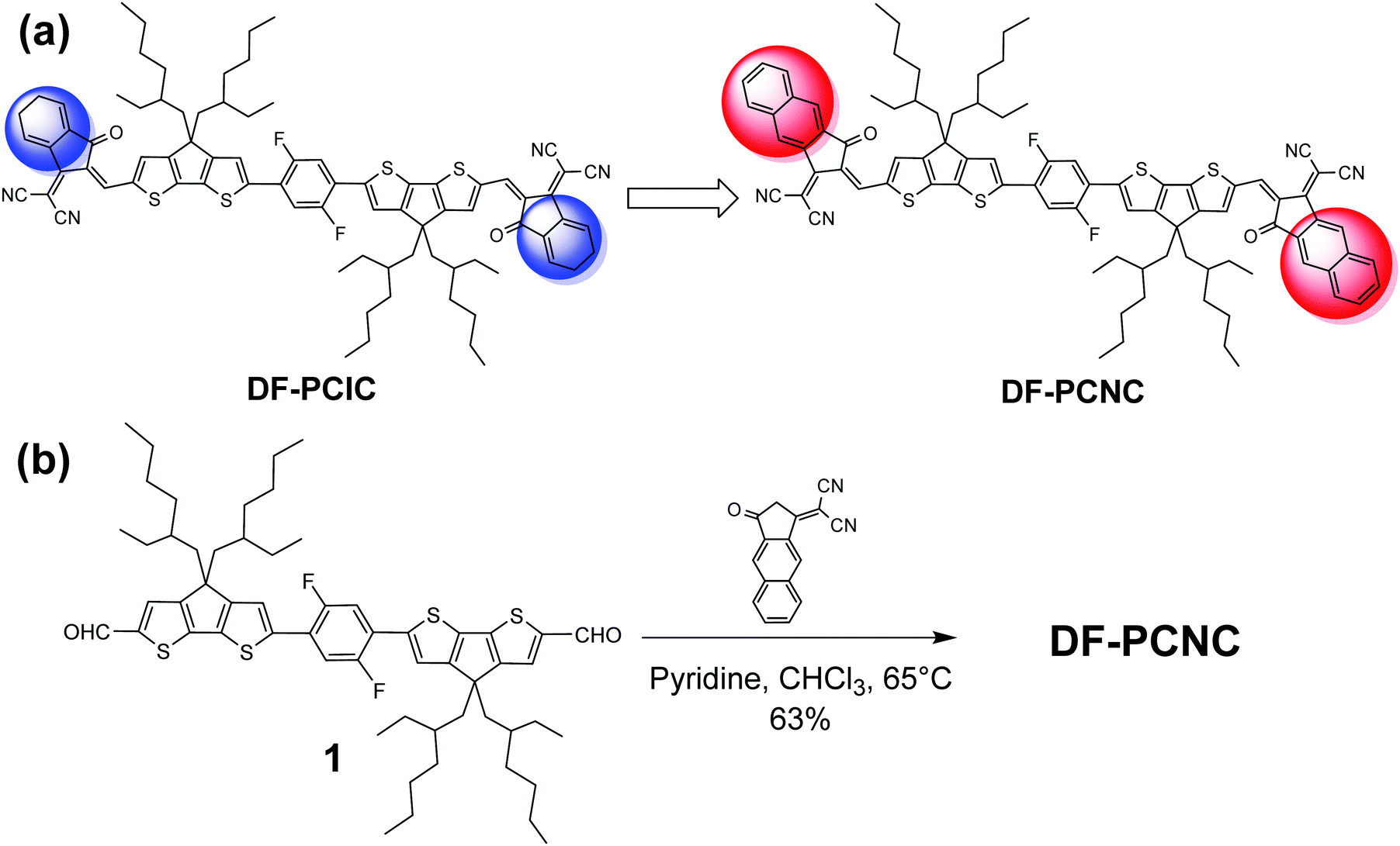 | ||
| Scheme 1 (a) The chemical structures of DF-PCIC and DF-PCNC. (b) The synthetic route to DF-PCNC. | ||
However, compared to those of OSCs employing non-fullerene acceptors with an all-fused ring core, the PCE of the DF-PCIC-based device is a little lower, which can be mainly ascribed to its smaller JSC.30,31 We think that there are two reasons responsible for the relatively lower JSC. Firstly, the absorption onset of DF-PCIC is located at about 781 nm, so that a large part of solar photons in the near-infrared region can’t be harvested. Secondly, from the UV-vis absorption spectrum of the DF-PCIC film, it is observed that the blue-shifted absorption peak representing H-aggregates (face-to-face arrangement of molecules) is stronger than the red-shifted one of J-aggregates (end-to-end arrangement of molecules).32–35 This self-assembly behavior is contrary to that of non-fullerene acceptors with an all-fused ring core, implying that π–π stacking of A terminals for DF-PCIC needs to be enhanced, in order to get better morphology of the donor:acceptor blended films favorable for exciton dissociation and charge carrier transport, thus, larger JSC for the relevant device can be achieved.
Taking the above considerations into account, in this work, we design and synthesize a new non-fullerene acceptor, DF-PCNC, by changing A end-groups from IC of DF-PCIC to NC. And the structure of DF-PCNC is shown in Scheme 1a. Then, we investigate the influences of π-conjugation expansion on DF-PCNC's absorptions, energy levels and molecular stacking. Finally, we fabricate the OSCs with DF-PCNC and PBDB-T as the acceptor and donor, respectively, and explore the relationship between photovoltaic performances and the blended films’ morphologies, to prove the rationality of our molecular design.
2. Results and discussion
2.1. Synthesis and characterization of DF-PCNC
As shown in Scheme 1b, DF-PCNC is synthesized through a Knoevenagel condensation reaction between compound 1 and NC, which are obtained according to the reported synthetic procedures.22,36 The chemical structure of DF-PCNC is fully characterized by 1H NMR, MALDI-TOF MS and elemental analysis. It is found that DF-PCNC exhibits good solubility only in chloroform (∼10 mg mL−1), whereas DF-PCIC is highly soluble in both chloroform and chlorobenzene. This phenomenon implies that the intermolecular interactions of DF-PCNC become stronger when the structure of A end-groups is enlarged from IC to NC.UV-vis absorption spectra of DF-PCNC and DF-PCIC in both chloroform solutions (Fig. 1a) and as-cast films (Fig. 1b) are measured and compared. As expected, DF-PCNC solution has stronger and more red-shifted absorptions with a maximum molar extinction coefficient (ε) of 2.45 × 10⁵ mol−1 L cm−1 at 700 nm while that of DF-PCIC is 1.96 × 10⁵ mol−1 L cm−1 at 670 nm. This changing tendency is also observed for the DF-PCNC as-cast film, and from its absorption onset at 807 nm, the narrower optical band gap (Eoptg) of DF-PCNC is calculated as 1.54 eV. Thus, DF-PCNC possesses intense absorptions in the range of 550–800 nm, which are complementary to those of the polymer donor, PBDB-T. Moreover, it is found that, for the DF-PCNC film, the absorption peak at 727 nm corresponding to J-aggregates (end-to-end arrangement of molecules) has a larger magnitude than that at 671 nm attributed to H-aggregates (face-to-face arrangement of molecules), which is in contrast to that of the DF-PCIC film. These results indicate that the conjugation extension of A terminals not only improves DF-PCNC's light-harvesting capability but also induces it to form stronger π–π stacking of A end-groups in the condensed state. This will undoubtedly enhance hopping transport of electrons between neighboring DF-PCNC molecules for the resulting OSCs.
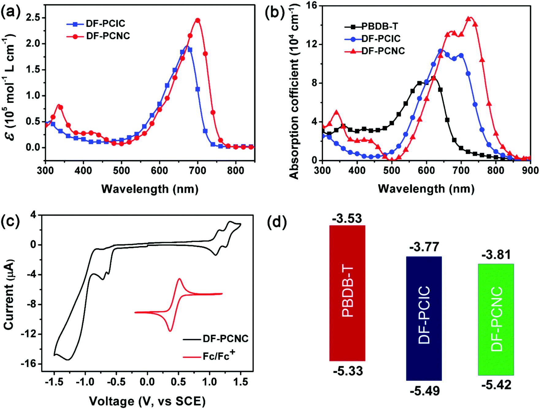 | ||
| Fig. 1 (a) UV-vis absorption spectra of DF-PCIC and DF-PCNC in chloroform solutions. (b) UV-vis absorption spectra of PBDB-T, DF-PCIC and DF-PCNC as-cast films. (c) Cyclic voltammograms of DF-PCNC and Fc/Fc+ in dichloromethane solutions. (d) The energy levels of PBDB-T, DF-PCIC and DF-PCNC. | ||
Cyclic voltammetry (CV) is done to measure the energy levels of DF-PCNC (Fig. 1c). From Fig. 1c, the onset reduction potential (Ered) and the onset oxidation potential (Eox) of DF-PCNC are found to be −0.55 and 1.06 V, respectively. Thus, the lowest unoccupied molecular orbital (LUMO) and the highest occupied molecular orbital (HOMO) energy levels are obtained as −3.81 and −5.42 eV, respectively. Compared to those of DF-PCIC (−3.77 and −5.49 eV), DF-PCNC has a slightly deeper LUMO and a little higher HOMO, which agrees to its narrower band gap disclosed by optical property characterization. Even so, the energy levels of DF-PCNC still match well with those of the polymer donor, PBDB-T (−3.53 and −5.33 eV),37 to prepare OSCs (Fig. 1d).
2.2. Photovoltaic performances of OSCs
To evaluate the photovoltaic properties of DF-PCNC, OSCs are fabricated with a structure of ITO/ZnO/PBDB-T:DF-PCNC/MoO3/Ag. All photovoltaic parameters of OSCs are summarized in Table 1 and Table S1 (ESI†). Firstly, we vary the weight ratios of the donor (D) and acceptor (A) from 1![[thin space (1/6-em)]](https://www.rsc.org/images/entities/char_2009.gif) :1 to 1:1.5, and find that the 1:1.2 ratio is the best composition. Under this condition, a PCE of 5.94% with a VOC of 0.90 eV, a JSC of 14.36 mA cm−2 and a FF of 44.98% is obtained for the OSC based on the as-cast blended film. Then, we employ two post-treatment methods, 1-chloronaphthalene (CN) additive and thermal annealing, to improve the device performance. We observe that the CN additive can greatly increase JSC and FF, leading to substantial enhancement of the PCEs of the resulting devices though VOC decreases to some extent. When the proportion of the CN additive is optimized as 1.2%, the OSC gives a high PCE of 10.85% with a VOC of 0.87 eV, a JSC of 17.63 mA cm−2 and a FF of 69.91%. After this device is further annealed at 100 °C for 10 minutes, the best PCE of 11.63%, with a VOC of 0.86 eV, a JSC of 18.16 mA cm−2 and a FF of 72.62%, is achieved. The relevant J–V curves are displayed in Fig. 2a. As expected, the PBDB-T:DF-PCNC-based OSCs provide a better PCE with a 16% higher JSC than the PBDB-T:DF-PCIC-based ones, and an excellent FF of over 72% is maintained. To our best knowledge, the PCE of 11.63% is the highest value for OSCs based on non-fullerene acceptors adopting decreased fused-ring D cores to date.
:1 to 1:1.5, and find that the 1:1.2 ratio is the best composition. Under this condition, a PCE of 5.94% with a VOC of 0.90 eV, a JSC of 14.36 mA cm−2 and a FF of 44.98% is obtained for the OSC based on the as-cast blended film. Then, we employ two post-treatment methods, 1-chloronaphthalene (CN) additive and thermal annealing, to improve the device performance. We observe that the CN additive can greatly increase JSC and FF, leading to substantial enhancement of the PCEs of the resulting devices though VOC decreases to some extent. When the proportion of the CN additive is optimized as 1.2%, the OSC gives a high PCE of 10.85% with a VOC of 0.87 eV, a JSC of 17.63 mA cm−2 and a FF of 69.91%. After this device is further annealed at 100 °C for 10 minutes, the best PCE of 11.63%, with a VOC of 0.86 eV, a JSC of 18.16 mA cm−2 and a FF of 72.62%, is achieved. The relevant J–V curves are displayed in Fig. 2a. As expected, the PBDB-T:DF-PCNC-based OSCs provide a better PCE with a 16% higher JSC than the PBDB-T:DF-PCIC-based ones, and an excellent FF of over 72% is maintained. To our best knowledge, the PCE of 11.63% is the highest value for OSCs based on non-fullerene acceptors adopting decreased fused-ring D cores to date.
| D/A ratio (by wt.) | CN (%) | Thermal annealinga | V OC (V) | J SC (mA cm−2) | FF (%) | PCEc (%) | |
|---|---|---|---|---|---|---|---|
| a Annealing for 10 minutes. b Values in parentheses are calculated from the corresponding EQE curves. c The best PCEs of the devices, and the values in parentheses are the average PCEs for 10 devices. d The data are cited from the previous work.22 | |||||||
| DF-PCNC | 1:1.2 |
— | — | 0.90 | 14.36 (14.10) | 44.98 | 5.94 (5.88) |
| 1.2 | — | 0.87 | 17.63 (17.14) | 69.91 | 10.85 (10.75) | ||
| 1.2 | 100 °C | 0.86 | 18.16 (17.62) | 72.62 | 11.63 (11.59) | ||
| DF-PCICd | 1:1.2 |
0.5 | 130 °C | 0.91 | 15.66 (15.37) | 72.07 | 10.14 (10.12) |
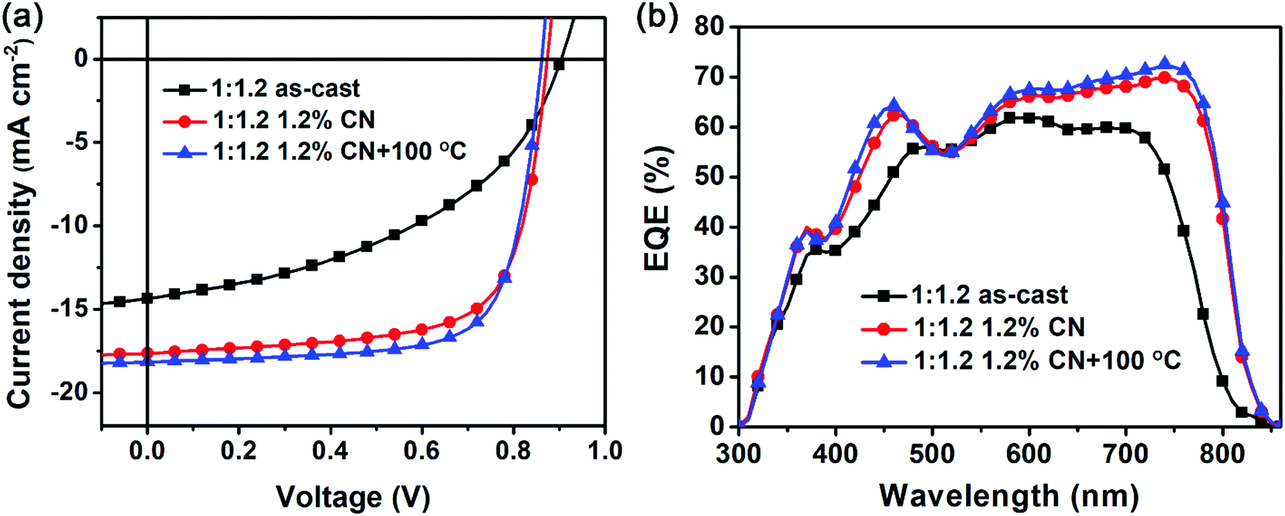 | ||
| Fig. 2 J–V curves (a) and EQE spectra (b) of the PBDB-T:DF-PCNC-based OSCs. | ||
The external quantum efficiency (EQE) spectra of the PBDB-T:DF-PCNC-based OSCs are shown in Fig. 2b. We can observe that the photoresponse range includes the absorptions from both donor and acceptor, suggesting that they both contribute to the photocurrents in OSCs. Furthermore, the CN additive and thermal annealing not only increase EQE values in all regions but also extend the photoresponse range to around 840 nm, resulting in the improvement of the JSCs. Thereby, the DF-PCNC-based device yields an obviously bigger JSC than the DF-PCIC-based one since its photoresponse range ends at ∼780 nm.22 In addition, it is worth pointing out that DF-PCNC shows the absorption spectrum expanded to a longer wavelength region than those of the previously reported non-fullerene acceptors with the same NC terminals; consequently, the DF-PCNC-based OSC gives a higher JSC than its counterparts.36,38 This indicates that the DFB ring connected with two CPDT moieties is a more appropriate D core paired with NC end-groups to construct high-performance non-fullerene acceptors.
2.3. Charge carrier mobilities of the blended films
The charge carrier mobilities of 1:1.2 PBDB-T:DF-PCNC blended films are investigated by the space-charge-limited current (SCLC) method, using a structure of ITO/PEDOT:PSS/PBDB-T:DF-PCNC/MoO3/Ag for hole-only devices, and a structure of ITO/ZnO/PFN/PBDB-T:DF-PCNC/PFN/Al for electron-only devices, respectively. It is observed that both hole and electron mobilities (μh and μe) of the PBDB-T:DF-PCNC blended films are higher than those of the PBDB-T:DF-PCIC films prepared under the same or similar conditions. From Fig. S4 (ESI†), for the as-cast PBDB-T:DF-PCNC film, μh and μe are obtained as 0.93 × 10⁻⁴ and 1.28 × 10⁻⁴ cm2 V−1 s−1, respectively, while those of the as-cast PBDB-T:DF-PCIC film are 0.15 × 10⁻⁴ and 0.10 × 10⁻⁴ cm2 V−1 s−1, respectively.22 After application of the CN additive, the PBDB-T:DF-PCNC film shows a sharply increased μh (2.72 × 10⁻⁴ cm2 V−1 s−1) and a slightly improved μe (1.42 × 10⁻⁴ cm2 V−1 s−1). Accordingly, the PBDB-T:DF-PCIC film possesses an enhanced μh (0.85 × 10⁻⁴ cm2 V−1 s−1) but a reduced μe (0.06 × 10⁻⁴ cm2 V−1 s−1).22 When the blended films are treated with both CN additive and thermal annealing, μh (6.51 × 10⁻⁴ cm2 V−1 s−1) and μe (1.97 × 10⁻⁴ cm2 V−1 s−1) of the PBDB-T:DF-PCNC film are still obviously better than those of the corresponding PBDB-T:DF-PCIC one (1.28 × 10⁻⁴ and 0.26 × 10⁻⁴ cm2 V−1 s−1).22 These results imply that the intermolecular π–π stacking of DF-PCNC is indeed stronger than that of DF-PCIC; meanwhile, the enhanced self-assembly of DF-PCNC promotes an orderly arrangement of PBDB-T molecules, leading to more efficient hole and electron transportation in OSCs, which is in accordance with the increased JSC and the high FF for the DF-PCNC-based devices.
2.4. The morphologies of the PBDB-T:DF-PCNC blended films
The molecular arrangements of the donor and acceptor in pristine and blended films are investigated by grazing-incidence wide-angle X-ray scattering (GIWAXS) measurements.39 The obtained two-dimensional (2D) scattering patterns and the out-of-plane and in-plane intensity profiles are presented in Fig. 3. We observe that the as-cast PBDB-T film displays a strong lamellar peak at 0.30 Å−1 (d = 21 Å) in the out-of-plane direction and a relatively weaker lamellar peak at 0.29 Å−1 in the in-plane direction, suggesting that pure PBDB-T prefers to adopt edge-on orientation in the film. And the as-cast DF-PCNC film shows a strong π–π stacking peak at 1.7 Å−1 (d = 3.7 Å) in the out-of-plane direction and a lamellae peak at 0.43 Å−1 (d = 15 Å) in the in-plane direction, which means that DF-PCNC mainly adopts face-on orientation in the film. For the as-cast PBDB-T:DF-PCNC blended film, the edge-on lamellae peak at 0.30 Å−1 of PBDB-T is maintained but the diffraction peaks of DF-PCNC are hardly observed, suggesting a significant decrease of the crystallinity of DF-PCNC in the as-cast blend film. Accordingly, the as-cast blended film shows relatively lower electron and hole mobilities, and thereby a lower PCE. As for the blended film treated with 1.2% CN additive, definite π–π stacking and lamellar peaks of face-on oriented DF-PCNC are observed, indicating the enhanced crystallinity of DF-PCNC due to the addition of CN. Furthermore, a new (200) lamellae peak of PBDB-T at 0.60 Å−1 in the out-of-plane direction is observed, implying that the crystallinity of PBDB-T is also improved. As a result, the blended film with the CN additive exhibits greatly increased electron and hole mobilities, leading to a much higher PCE with enhanced JSC and FF and an extended photoresponse range for the corresponding OSC. It should also be noted that the enhanced crystallinity of DF-PCNC can lead to a narrowing of the band gap and a decrease of the LUMO energy level. Because the VOC of OSCs is proportional to the difference between the LUMO of the acceptor and the HOMO of the donor, the VOC of the corresponding device decreases to some extent. For the blended film processed with 1.2% CN additive and thermal annealing at 100 °C for 10 minutes, the crystallinity of both DF-PCNC and PBDB-T is further increased, providing the highest electron and hole mobilities. Therefore, the best PCE of 11.63% is achieved for the resultant device.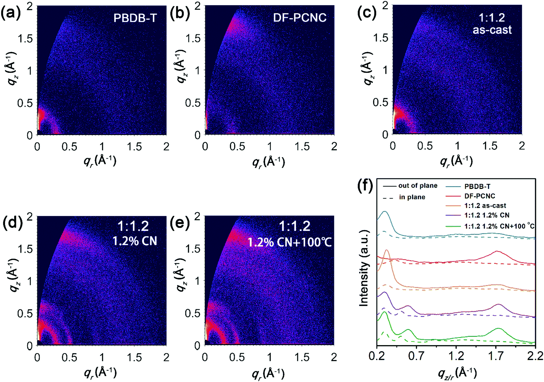 | ||
| Fig. 3 2D GIWAXS images of the as-cast PBDB-T film (a), the as-cast DF-PCNC film (b), the as-cast PBDB-T:DF-PCNC blended film (c), the PBDB-T:DF-PCNC blended film processed with 1.2% CN (d), and the PBDB-T:DF-PCNC blended film processed with 1.2% CN and thermal annealing at 100 °C for 10 minutes (e). (f) 1D out-of-plane (solid lines) and in-plane (dotted lines) X-ray profiles extracted from GIWAXS patterns. | ||
Grazing-incidence small-angle X-ray scattering (GISAXS) measurements are carried out to characterize phase-separation information in the blended films.40 2D GISAXS patterns and the corresponding in-plane intensity profiles are shown in Fig. S5 (ESI†) and Fig. 4, respectively. We adopt the Debye–Anderson–Brumberger (DAB) model and a fractal-like network model to account for the scattering contribution from intermixing amorphous phases and acceptor domains, respectively, and estimate the corresponding domain sizes by fitting. From Fig. 4, the sizes of the intermixing region (ξ) and pure acceptor (2Rg) in the as-cast PBDB-T:DF-PCNC blended film are 23 and 4.1 nm, respectively. As for the blended film treated with 1.2% CN additive, the size of the intermixing region decreases to 19 nm and that of the acceptor phase increases to 6.3 nm. For the blended film processed with 1.2% CN additive and thermal annealing at 100 °C, the size of the intermixing region is 20 nm and 2Rg of the acceptor phase increases further to 8.4 nm, which is attributed to the enhanced crystallization of DF-PCNC. When both donor and acceptor domain sizes are in the appropriate range for efficient exciton dissociation, an increase of acceptor domain size can reduce the non-radiative recombination and facilitate electron transport,41 in agreement with the observed trend of device performance improvement.
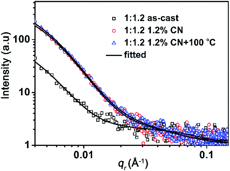 | ||
| Fig. 4 GISAXS in-plane intensity profiles of the PBDB-T:DF-PCNC blended films. | ||
The morphologies of PBDB-T:DF-PCNC blended films are further investigated by atomic force microscopy (AFM). The relevant images are shown in Fig. S6 (ESI†). We observe that the as-cast blended film is relatively smooth with a root mean square (RMS) roughness of 0.895 nm. For the blended film processed with the CN additive, the RMS roughness increases to 1.41 nm because of the improved crystallinity of PBDB-T and DF-PCNC. After the CN additive and thermal annealing are both employed, the film becomes even rougher with a RMS roughness of 1.45 nm because the self-assemblies of the donor and acceptor are further enhanced. This trend is also proven by transmission electron microscopy (TEM) characterization. As seen in Fig. S6 (ESI†), the as-cast film is relatively uniform and no obvious phase-separation is found. For the blended film treated with the CN additive, nanoscaled phase-separation domains are formed, and even some nanofibers are observed. After the combination treatments of the CN additive and thermal annealing, more nanofibers with greater length emerge, which is ascribed to the substantial improvement in the orderly arrangement of PBDB-T main chains. The above results explain perfectly why the CN additive and thermal annealing improve the photovoltaic performances, and especially hole mobility is enhanced with a larger magnitude than electron mobility in the corresponding devices.
3. Conclusions
In conclusion, we design and synthesize a new non-fullerene acceptor with a decreased fused-ring D core, DF-PCNC, by replacing the IC terminal groups of DF-PCIC with NC groups of extended π-conjugation. DF-PCNC possesses stronger and more red-shifted absorption peaks than DF-PCIC. In addition, NC groups enhance the π–π stacking between DF-PCNC molecules. These characteristics not only improve the light-harvesting capability, but also promote self-assembly behaviors of the films obtained by blending DF-PCNC with the polymer donor, PBDP-T. Through a series of GIWAXS, GISAXS, TEM and AFM characterizations, it is proved that the CN additive and thermal annealing can lead to good morphologies of the blended films, i.e. donor and acceptor phases with high crystallinity are formed with sizes favorable for charge generation and transport. Therefore, the PBDB-T:DF-PCNC OSCs provide a higher PCE of 11.63% with increased JSC and unchangeable FF while compared to the PBDB-T:DF-PCIC ones. The above results demonstrate that the enhancement of π–π stacking between end-groups is an efficient method for improving the photovoltaic properties of non-fullerene acceptors, and the decreased fused-ring D core through the connection of smaller building blocks via intramolecular noncovalent interactions can also be used to construct high-performance non-fullerene acceptors.Conflicts of interest
There are no conflicts to declare.Acknowledgements
This work was supported by the National Natural Science Foundation of China (No. 21734008, 21474088, 51473142, 51561145001, 51620105006, 61721005), the 973 Program (2014CB643503), and Zhejiang Province Science and Technology Plan (No. 2018C01047). X. Lu acknowledges the financial support from the Research Grant Council of Hong Kong (General Research Fund No. 14314216).Notes and references
- S. Li, Z. Zhang, M. Shi, C.-Z. Li and H. Chen, Phys. Chem. Chem. Phys., 2017, 19, 3440–3458 RSC.
- S. Li, W. Liu, C.-Z. Li, M. Shi and H. Chen, Small, 2017, 13, 1701120 CrossRef PubMed.
- S. Zhang, Y. Qin, J. Zhu and J. Hou, Adv. Mater., 2018, 30, 1800868 CrossRef PubMed.
- S. Li, L. Ye, W. Zhao, H. Yan, B. Yang, D. Liu, W. Li, H. Ade and J. Hou, J. Am. Chem. Soc., 2018, 23, 7159–7163 CrossRef PubMed.
- Y. Lin, J. Wang, Z. G. Zhang, H. Bai, Y. Li, D. Zhu and X. Zhan, Adv. Mater., 2015, 27, 1170–1174 CrossRef PubMed.
- Z. Fei, F. D. Eisner, X. Jiao, M. Azzouzi, J. A. Rohr, Y. Han, M. Shahid, A. S. R. Chesman, C. D. Easton, C. R. McNeill, T. D. Anthopoulos, J. Nelson and M. Heeney, Adv. Mater., 2018, 30, 1705209 CrossRef PubMed.
- Y. Liu, Z. Zhang, S. Feng, M. Li, L. Wu, R. Hou, X. Xu, X. Chen and Z. Bo, J. Am. Chem. Soc., 2017, 129, 3356–3359 CrossRef PubMed.
- P. Ye, Y. Chen, J. Wu, X. Wu, S. Yu, W. Xing, Q. Liu, X. Jia, A. Peng and H. Huang, J. Mater. Chem. C, 2017, 5, 12591–12596 RSC.
- W. Bai, X. Xu, Q. Li, Y. Xu and Q. Peng, Small Methods, 2018, 2, 1700373 CrossRef.
- Y. Wu, H. Bai, Z. Wang, P. Cheng, S. Zhu, Y. Wang, W. Ma and X. Zhan, Energy Environ. Sci., 2015, 8, 3215–3221 RSC.
- S. Holliday, R. S. Ashraf, A. Wadsworth, D. Baran, S. A. Yousaf, C. B. Nielsen, C. Tan, S. D. Dimitrov, Z. Shang, N. Gasparini, M. Alamoudi, F. Laquai, C. J. Brabec, A. Salleo, J. R. Durrant and I. McCulloch, Nat. Commun., 2016, 7, 11585–11595 CrossRef PubMed.
- S. Dai, F. Zhao, Q. Zhang, T. K. Lau, T. Li, K. Liu, Q. Ling, C. Wang, X. Lu, W. You and X. Zhan, J. Am. Chem. Soc., 2017, 3, 1336–1343 CrossRef PubMed.
- S. Li, W. Liu, C.-Z. Li, T.-K. Lau, X. Lu, M. Shi and H. Chen, J. Mater. Chem. A, 2016, 4, 14983–14987 RSC.
- F. Liu, Z. Zhou, C. Zhang, T. Vergote, H. Fan, F. Liu and X. Zhu, J. Am. Chem. Soc., 2016, 38, 15523–15526 CrossRef PubMed.
- Y. Lin, Q. He, F. Zhao, L. Huo, J. Mai, X. Lu, C. J. Su, T. Li, J. Wang, J. Zhu, Y. Sun, C. Wang and X. Zhan, J. Am. Chem. Soc., 2016, 138, 2973–2976 CrossRef PubMed.
- N. Qiu, H. Zhang, X. Wan, C. Li, X. Ke, H. Feng, B. Kan, H. Zhang, Q. Zhang, Y. Lu and Y. Chen, Adv. Mater., 2017, 29, 1604964 CrossRef PubMed.
- X. Shi, L. Zuo, S. B. Jo, K. Gao, F. Lin, F. Liu and A. K. Jen, Chem. Mater., 2017, 29, 8369–8376 CrossRef.
- H. Yao, L. Ye, J. Hou, B. Jang, G. Han, Y. Cui, G. M. Su, C. Wang, B. Gao, R. Yu, H. Zhang, Y. Yi, H. Y. Woo, H. Ade and J. Hou, Adv. Mater., 2017, 29, 1700254 CrossRef PubMed.
- Y. Yang, Z.-G. Zhang, H. Bin, S. Chen, L. Gao, L. Xue, C. Yang and Y. Li, J. Am. Chem. Soc., 2016, 138, 15011–15018 CrossRef PubMed.
- Y. Lin, F. Zhao, Q. He, L. Huo, Y. Wu, T. C. Parker, W. Ma, Y. Sun, C. Wang, D. Zhu, A. J. Heeger, S. R. Marder and X. Zhan, J. Am. Chem. Soc., 2016, 138, 4955–4961 CrossRef PubMed.
- G. Zhang, G. Yang, H. Yan, J. H. Kim, H. Ade, W. Wu, X. Xu, Y. Duan and Q. Peng, Adv. Mater., 2017, 29, 1606054 CrossRef PubMed.
- S. Li, L. Zhan, F. Liu, J. Ren, M. Shi, C.-Z. Li, T. P. Russell and H. Chen, Adv. Mater., 2018, 30, 1705208 CrossRef PubMed.
- T. L. Nguyen, H. Choi, S. J. Ko, M. A. Uddin, B. Walker, S. Yum, J. E. Jeong, M. H. Yun, T. J. Shin, S. Hwang, J. Y. Kim and H. Y. Woo, Energy Environ. Sci., 2014, 7, 3040–3051 RSC.
- A. C. Stuart, J. R. Tumbleston, H. Zhou, W. Li, S. Liu, H. Ade and W. You, J. Am. Chem. Soc., 2013, 135, 1806–1815 CrossRef PubMed.
- Z. Zhang, S. Zhang, Z. Liu, Z. Zhang, Y. Li, C.-Z. Li and H. Chen, Acta. Phys.-Chim. Sin., 2019, 35, 394–400 Search PubMed.
- L. Zhan, S. Li, H. Zhang, F. Gao, T.-K. Lau, X. Lu, D. Sun, P. Wang, M. Shi, C.-Z. Li and H. Chen, Adv. Sci., 2018 DOI:10.1002/advs.201800755.
- S. Li, L. Zhan, W. Zhao, S. Zhang, B. Ali, Z. Fu, T.-K. Lau, X. Lu, M. Shi, C.-Z. Li, J. Hou and H. Chen, J. Mater. Chem. A, 2018, 6, 12132–12141 RSC.
- H. Huang, L. Yang, A. Facchetti and T. J. Marks, Chem. Rev., 2017, 117, 10291–10318 CrossRef PubMed.
- T. Dong, L. Lv, L. Feng, Y. Xia, W. Deng, P. Ye, B. Yang, S. Ding, A. Facchetti, H. Dong and H. Huang, Adv. Mater., 2017, 29, 1606025 CrossRef PubMed.
- S. Li, L. Ye, W. Zhao, S. Zhang, S. Mukherjee, H. Ade and J. Hou, Adv. Mater., 2016, 28, 9423–9429 CrossRef PubMed.
- W. Zhao, D. Qian, S. Zhang, S. Li, O. Inganas, F. Gao and J. Hou, Adv. Mater., 2016, 28, 4734–4739 CrossRef PubMed.
- Q. Wu, D. Zhao, J. Yang, V. Sharapov, Z. Cai, L. Li, N. Zhang, A. Neshchadin, W. Chen and L. Yu, Chem. Mater., 2017, 29, 1127–1133 CrossRef.
- Z. Yan, H. Xu, S. Guang, X. Zhao, W. Fan and X. Y. Liu, Adv. Funct. Mater., 2012, 22, 345–352 CrossRef.
- G. Liu, J. Sheng, H. Wu, C. Yang, G. Yang, Y. Li, R. Ganguly, L. Zhu and Y. Zhao, J. Am. Chem. Soc., 2018, 140, 6467–6473 CrossRef PubMed.
- G. Han, Y. Guo, X. Song, Y. Wang and Y. Yi, J. Mater. Chem. C, 2017, 5, 4852–4857 RSC.
- S. Li, L. Ye, W. Zhao, X. Liu, J. Zhu, H. Ade and J. Hou, Adv. Mater., 2017, 29, 1704051 CrossRef PubMed.
- D. Qian, L. Ye, M. Zhang, Y. Liang, L. Li, Y. Huang, X. Guo, S. Zhang, Z. Tan and J. Hou, Macromolecules, 2012, 45, 9611–9617 CrossRef.
- H. Feng, N. Qiu, X. Wang, Y. Wang, B. Kan, X. Wan, M. Zhang, A. Xia, C. Li, F. Liu, H. Zhang and Y. Chen, Chem. Mater., 2017, 29, 7908–7917 CrossRef.
- J. Mai, H. Lu, T.-K. Lau, S. H. Peng, C. S. Hsu, W. Hua, N. Zhao, X. Xiao and X. Lu, J. Mater. Chem. A, 2017, 23, 11739–11745 RSC.
- J. Mai, T.-K. Lau, J. Li, S. H. Peng, C. S. Hsu, U. S. Jeng, J. Zeng, N. Zhao, X. Xiao and X. Lu, Chem. Mater., 2016, 17, 6186–6195 CrossRef.
- H. Zhang, X. Wang, L. Yang, S. Zhang, Y. Zhang, C. He, W. Ma and J. Hou, Adv. Mater., 2017, 29, 1703777 CrossRef PubMed.
Footnotes |
| † Electronic supplementary information (ESI) available: Materials and methods, synthesis details, NMR and MS spectra, TGA, DSC, SCLC, GISAXS and AFM images, etc. See DOI: 10.1039/c8qm00318a |
| ‡ These authors contributed equally to this work. |
| This journal is © the Partner Organisations 2018 |