
 Open Access Article
 This Open Access Article is licensed under a Creative Commons Attribution-Non Commercial 3.0 Unported Licence
Self-organisation and characterisation of hierarchical structures in trimethyl β-cyclodextrin nano-films†
S.
Ogawa
 ab,
K.
Ashida
c,
T.
Kaneko
c and
I.
Takahashi
*a
ab,
K.
Ashida
c,
T.
Kaneko
c and
I.
Takahashi
*a
aDepartment of Physics, School of Science and Technology, Kwansei Gakuin University, Sanda 669-1337, Japan. E-mail: suikyo@kwansei.ac.jp
bDepartment of Materials and Life Science, Faculty of Science and Technology, Seikei University, 3-3-1 Kichijojikitamachi, Musashino-shi, Tokyo 180-8633, Japan
cDepartment of Nanotechnology for Sustainable Energy, Science and Technology, Kwansei Gakuin University, Sanda 669-1337, Japan
First published on 13th August 2018
Abstract
Despite the numerous materials that have been developed, controlling the self-organisation and detailed characterisation of hierarchical nanostructures composed of various functional molecular units remains a challenging task. Herein, we report a facile approach for creating flat nanosheets and helical nanofibres for ultrathin films (ca. 12 nm) and thin films (ca. 120 nm), respectively. These films contain a member of the cyclodextrin family, trimethyl β-cyclodextrin (TMCD), and form via self-organisation with heating (thermal annealing) in the absence of both polymeric components and organic solvent. X-ray reflectivity (XRR) and grazing-incident-angle X-ray diffraction (GIXD) readily explain the characteristic molecular assembling behaviour in the thin films, such as the highly perpendicularly ordered polycrystalline structure of the nanosheet crystal films and the dewetting behaviour for the fabrication of bundled nanofibres. In addition to X-ray analysis, scanning electron microscopy (SEM) and atomic-force microscopy (AFM) imaging reveals that the obtained nanofibres are well rounded and partially double or triple-helical coiled, with highly frustrated characteristics. The surface homogeneity prior to the thermal annealing was found to be crucial to determine the creation of the helical nanofibre structure. Also, the results suggest the importance of the absence of solvent vapour for the creation of the helical nanofibres. Thus, this report proposes a facile self-organisation process for creating polymer-free cyclodextrin-based nanostructures that should have wide applications. It also shows the effectiveness of X-ray analyses combined with several surface-sensitive X-ray techniques and microscopy observations.
Introduction
Cyclodextrins (CDs) contain hydrophobic cavities that endow them with a special ability to accommodate many organic compounds by inclusion complexation.1–3 Noncovalent inclusion complexes of CDs with a variety of guest molecules, including small-molecule guests and higher-molecular-weight guest polymers, have been eagerly investigated. By forming noncovalent inclusion complexes and by the coalescence of guest polymers in their complexes, sophisticated nanostructured and functionalised polymers that are distinct from their bulk materials have been obtained from solutions and melts of CDs.4–7Over the past few years, nanofibres containing CDs or their inclusion compounds with low- or high-molecular-weight guests have been widely reported;8 they are classified into four types: polymer/CD nanofibres, carrier-free CD nanofibres, polymer/CD-inclusion complex nanofibres and polymer/polymer/CD-inclusion complex nanofibres. By using CD technology, higher crystallinity and crystallizability have been achieved compared with nanofibres formed from neat polymers.
CD nanostructuring without the addition of polymeric components has been achieved due to the superior aggregation (entanglement) behaviour of CDs themselves.9–19 Celebioglu et al. first prepared polymer-free CD nanofibres by electrospinning methyl β-cyclodextrin (MCD) from both dimethylformamide (DMF) and water solutions.9 Later, several CDs, such as hydroxypropyl β-CD,10–13 unmodified γ-CD,14 and native CDs15 such as α-CD and β-CD, were used with similar solvents to create electrospinning polymer-free CD nanofibres. Due to their unoccupied cavities, these CD nanofibres can capture organic pollutants14 and antioxidants that are feasible for deterioration,16 and they can be used as templates to yield metal-oxide tubes,17etc.8,18,19 Conversely, the preparation of nanosheets without adding polymeric carriers was reported recently by Rajendiran.7 Despite the development of polymer-free CD technology, less attention has been paid to the formation of helical nanofibre structures by polymer-free CDs, although these helical properties may have wide applications in addition to the remaining unoccupied cavities. Fabrication of chiral nanostructures is a recent research topic with potential applications based on chirality because of their characteristic mechanical, electromagnetic, optical and catalytic properties.20–24 Also, the preparation of wide-area nanosheets, which can be used as sensing devices, has not yet been achieved.
Meanwhile, many reports discuss the controlled self-organisation of materials consisting of chiral nanostructures, such has helical nanofibers, by the aggregation of chiral components.20–35 Among these, self-organisation methodologies by crystallisation from low-dimensional matrices such as ultrathin films is a widely studied strategy.25–34 Occasionally, nanosheet structures are observed for thinner polymer films,25,27,29,32,34,35 and structural correlations between nanosheet formation and helical nanofibre structures have been reported.27,29,31,35 Conversely, the formation of chiral assemblies consisting of cyclodextrin without polymeric additives and sophisticated substitutes in ultrathin films has not been investigated; however, the cyclodextrin unit is a chiral component because its sugar units are chiral.
In this paper, we report the self-organisation behaviour of trimethyl β-cyclodextrin (TMCD) in nano-thin films. TMCD possesses a per-methylated structure without hydroxyl group carriers (Chart 1). This CD is frequently used as a good candidate for complex inclusion.36–38 Also, several physicochemical properties of this CD have been extensively reported (Chart 1).36–44 In addition, we recently found that TMCD exhibits excellent solution processability toward homogeneous nanofilms on Si(100) substrates by spin-coating from a chloroform solution.45 The glass transition temperature Tg of a variety of polymeric films changes with the film thickness because of the confinement effect.46–48 However, the Tg values for TMCD ultrathin films (>2.4 nm thick) were detected at similar temperatures to those of TMCD bulk samples,45 suggesting that the TMCD molecules in the ultrathin films may show behaviour similar to that in the bulk powder state. Because the crystallisation conditions in the bulk state were reported by Tsukushi et al.,39,40 self-assembly behaviour of TMCD via crystallisation in ultrathin films, even less than 200 nm thick, was expected to be achieved because TMCD can exhibit crystallisation behaviour in thin films similar to that in bulk. To characterise this self-assembly and self-organisation behaviour, we used several X-ray techniques. Many X-ray analytical techniques can be achieved by changing the experiment mode and setup (with and without synchrotron radiation). In particular, X-ray reflectivity (XRR) can detect the thickness, roughness and electron density of films49,50 and can be very useful to analyse thin films, including amorphous sugar nano-films.45,51 Also, even for ultrathin films, conventional powder X-ray diffraction (PXRD) can detect diffraction when the crystallinity is high, although the use of a high power or a coherent beam is preferred if the structure is not destroyed by the intense radiation. The use of synchrotron radiation can readily overcome the difficulties caused by the low power of conventional X-ray sources.52 In each case, the appropriate adaptation or combination of these various X-ray analytical techniques can deepen our understanding of molecular assembly and organisation behaviours not only for amorphous samples but also for crystalline samples. Therefore, we applied XRR (Fig. 1) in addition to microscopy observations, including scanning electron microscopy (SEM) and atomic-force microscopy (AFM). With synchrotron radiation, we used grazing-incident X-ray diffraction (GIXD) with a two-dimensional (2D) detector. Also PXRD with commercial X-ray source was used to understand the crystallisation behaviour, crystallinity and alignment of the molecular assembly.
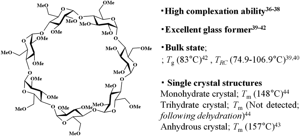 | ||
| Chart 1 Chemical structure of TMCD and its related properties. Tg; glass transition temperature, TRC; recrystallisation temperature, Tm; melting point. | ||
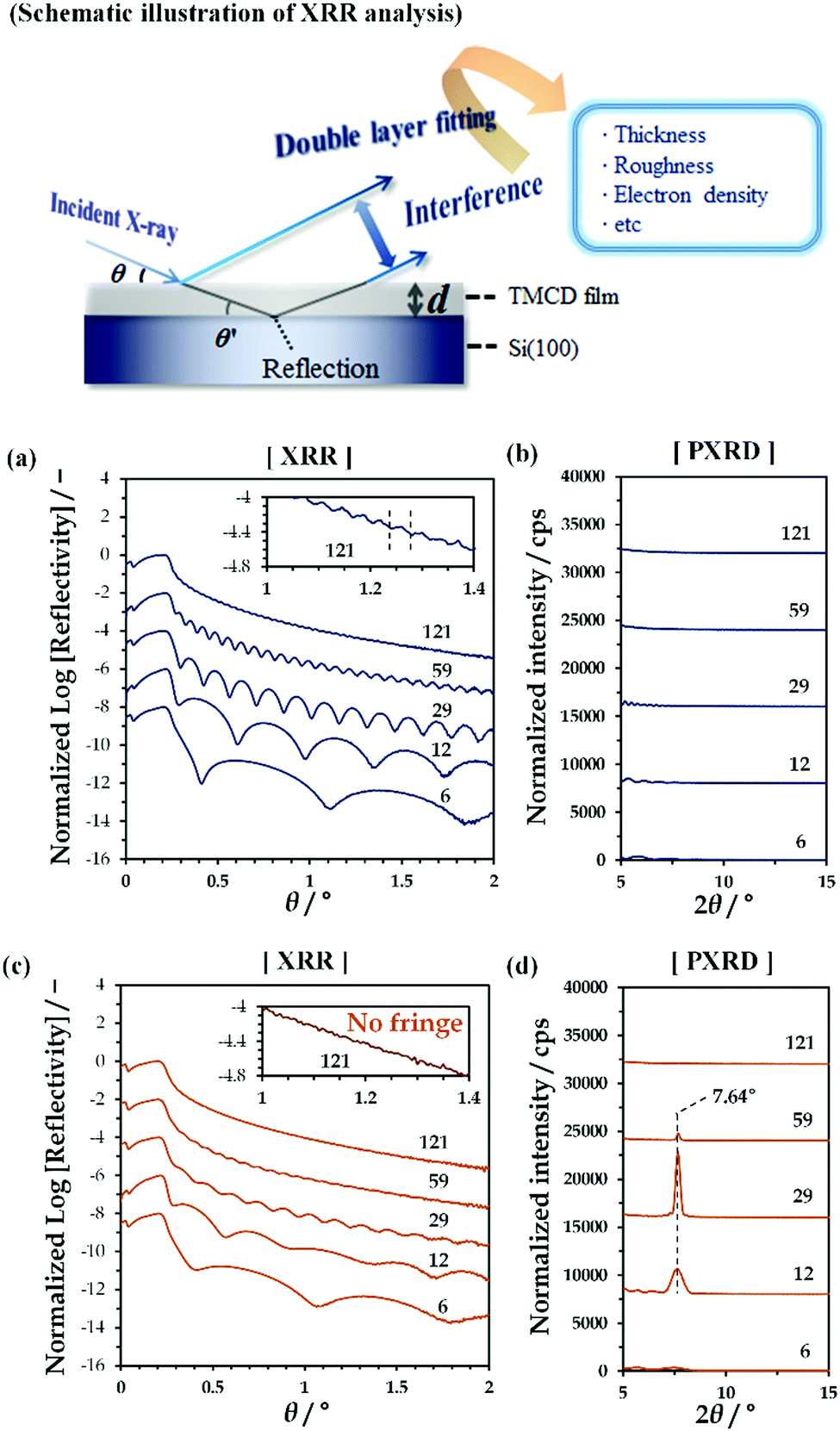 | ||
| Fig. 1 (a and c) XRR profiles and (b and d) PXRD profiles obtained for TMCD films with different film thicknesses (a, b) before and (c, d) after thermal annealing at 120 °C for 24 h. The initial film thickness in nm is depicted in each figure, and the insets of panels (a) and (c) show enlarged figures for the thickest film. | ||
Experiment
Self-organisation of TMCD hierarchical structures on Si substrate
Trimethyl β-cyclodextrin (TMCD; Mw: 1429.55) with high purity greater than 98% was purchased from TCI. Co. Ltd (Tokyo, Japan). It was further purified prior to use because the presence of differently hydrated samples can affect the crystallisation behaviour. A 20 wt% aqueous TMCD solution was prepared and heated to 90 °C for 1 h, leading to a TMCD precipitate.53 Subsequently, the precipitate was obtained by hot filtration. Filtered TMCD after recrystallising from hot aqueous solution showed a single melting behaviour in its heating thermogram at approximately 156 °C (Fig. S1, ESI†), which indicates that the purified TMCD consisted of monohydrate crystal (reference Tm = 157 °C,44 157.6 °C39). Thus, the monohydrate sample was used to prepare the sample solution after the filtrate was dried on filter paper and vacuum-dried overnight. Si(100) substrates (thickness ca. 525 μm) purchased from Electronics and Materials Corp. (Hyogo, Japan) were cut into 2 × 2 cm2 squares.TMCD chloroform solutions were prepared by dissolving purified TMCD in chloroform through ultrasonication for 5 min at room temperature. Subsequently, to develop the precursor film, the solution was spin-coated at 4000 rpm for 45 s onto a 2 × 2 cm2 Si(100) wafer that had been cleaned by washing with ethanol prior to spin-coating.45
The pristine TMCD films were dried under vacuum at ambient temperature for 1 h. Subsequently, the sample was quickly transferred to a vacuum drying oven (SVD30P, Sansyo Co. Ltd, Osaka, Japan) which was preheated to the desired temperature. To avoid overshooting the annealing temperature, the pristine TMCD films were placed in a desiccator after the temperature in the desiccator become constant. After thermal annealing, the door of the desiccator was opened at room temperature and the samples were obtained.
Characterisation of TMCD films deposited on Si substrate
X-ray analyses were performed using a multipurpose X-ray diffraction system equipped with a conventional X-ray source (Cu Kα, wavelength = 0.1542 nm) (SmartLab, Rigaku Corp., Tokyo, Japan) and by using the BL03XU beamline54 with a synchrotron radiation source (wavelength = 0.1 nm) at SPring-8 in Hyogo, Japan. With the former apparatus, specular XRR and PXRD profiles were obtained by 2θ/ω scanning under vacuum. The film thicknesses were determined from the XRR profiles in the low-angle range by fitting with software developed in-house that uses a recursive method based on dynamic scattering theory.55 The full width at half maximum (FWHM) of the PXRD profile around 7.64° was analysed by Gaussian peak adjustment using Origin 6.1 data analysis software (OriginLab Corp., USA). At BL03XU, a GIXD measurement was made, and diffraction patterns in the 0° to 18° range were obtained using an image-plate detector (R-AXIS IV, Rigaku Corp., Tokyo, Japan) with an incident angle of 0.1°. Measurements consisted of 30 s irradiation in He atmosphere, and the data analysis was performed using Fit2D.56 The surface topographies of the TMCD films were probed under ambient atmosphere using dynamic mode AFM with a SPM-9600 instrument (Shimadzu Co., Kyoto, Japan). Also, SEM images of the morphologies of the TMCD films were obtained in both Inlens (SE1) and SE2 modes using a Carl Zeiss Supra 40 instrument (Oberkochen, Germany) at low voltage without sputtering and under high vacuum conditions.Results and discussion
Self-organisation from noncrystalline TMCD film by thermal annealing
By spin-coating chloroform solutions containing dissolved TMCD monohydrate crystal onto Si(100) substrates, ultrathin TMCD nano-films with varying film thicknesses were prepared. As indicated by the clear Kiessig fringes in the XRR profiles [Fig. 1(a)], the TMCD films with thicknesses ranging from 6 to 121 nm showed excellent homogeneities, as similarly observed in our previous studies.45 In their PXRD profiles, no distinct diffraction peaks assigned to the formation of crystals were observed, clearly showing the noncrystalline structures of the films [Fig. 1(b)]. For these films, isothermal annealing was conducted to induce self-organisation.Fig. 1(c) and (d) show the XRR and PXRD profiles, respectively, for the TMCD films after annealing at 120 °C for 24 h; heating at 120 °C with an annealing time of over 12 h was determined to be the optimised conditions to develop the TMCD molecular assembly in the amorphous films, as determined from the appearance of the most intense diffraction peak in the X-ray diffraction (XRD) profile of the TMCD film with ca. 12 nm film thickness (Fig. S2, ESI†).
As shown in Fig. 1(c), the XRR fringes become unclear for the TMCD films thicker than ca. 59 nm compared with the fringes before annealing. Eventually, for the TMCD film with ca. 121 nm thickness, no distinct fringes are discernible, indicating the inhomogeneity of the TMCD film. However, even after annealing, fringes were recognised for the TMCD films thinner than 59 nm. Interestingly, despite the presence of these fringes, as shown in Fig. 1(d), below ca. 30 nm, the peak intensity and the sharpness of the Bragg reflections increased as the initial film thickness increased, whereas these quantities decreased as the film thickness further increased above ca. 59 nm. However, visual inspection revealed the formation of a hierarchical structure, which presumably reflects an inhomogeneous film structure. These conflicting results between the peak intensities of the Bragg reflection signals and the visual inspection arise from the difference in hierarchical assemblies, which will be discussed later.
Characterisation of the hierarchical structure evolved in thinner films
Fig. 2(a) shows the 2D-GIXD results for the TMCD films (ca. 12 nm) before and after thermal annealing. In this measurement, a synchrotron radiation source was used; however, no distinct reflection spot was observed before annealing [Fig. 2(a), top], reasonably indicating the lack of crystalline translational symmetry in the film before thermal annealing. Conversely, in the 2D-GIXD profile of the TMCD film after annealing, numerous reflection spots appeared [Fig. 2(a), bottom]. Also, streak spacing lines, similar to the reflection high energy electron diffraction (RHEED) pattern, appeared, indicating the formation of a heteroepitaxially layered structure.57 Note that the 2D diffraction pattern measured after the annealing is similar to a so-called rotation photograph with a single crystal rotated along the vertical axis, although we never rotated the sample during the exposure. This clearly indicates that the crystallites in the films are highly aligned along the direction normal to the substrate but are randomly distributed in the in-plane direction.58 At a glance, the reflection spots suggest an orthorhombic system due to the orthogonal locations of these spots in the 2D-GIXD profile.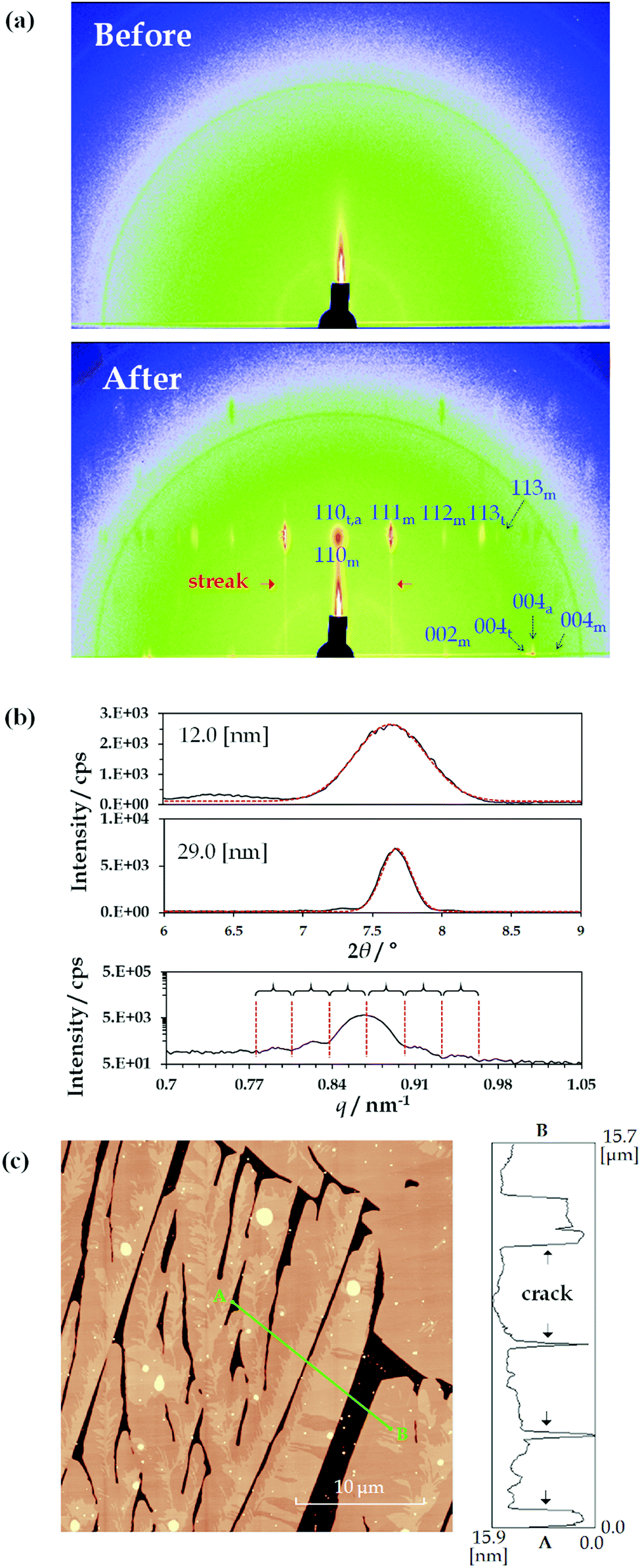 | ||
| Fig. 2 Characterisation of TMCD thin films. (a) 2D-GIXD results (top) before and (bottom) after thermal annealing at 120 °C for 24 h. Representative reflection spots were assigned by the Miller indices of the monohydrate, trihydrate, or anhydrous forms. Each is denoted with the subscript m, t, or a, respectively. (b) Experimental profiles and Gaussian fitting profiles of the PXRD peak around 7.64° for TMCD films ca. 12 and 29 nm thick. Most of the area under the experimental PXRD profile as a function of q was described by a logarithmical expression to make the Laue reflections findable. (c) AFM image of the TMCD film after thermal annealing. | ||
Meanwhile, the TMCD crystals, including the anhydrous, monohydrate and trihydrate forms, were reported as orthorhombic systems; the monohydrate structure has the unit cell parameters44a = 14.818 Å, b = 19.362 Å and c = 26.51 Å; the trihydrate structure has the unit cell parameters44a = 16.2051 Å, b = 16.287 Å and c = 30.0989 Å; and the anhydrous structure has the unit cell parameters43a = 15.9509 Å, b = 16.5772 Å and c = 28.9413 Å. In the 2D-GIXD profile for the TMCD film after annealing, the largest d values of the diffraction spot in the 90° azimuth were around 11.7 Å; in the 0° azimuth, they were around 13.3 Å. These d spacings correspond well to those of the (110) and (002) indices of the monohydrate form, which satisfy the orthogonal relationship of these Miller indices. Therefore, the presence of the monohydrate crystal form is strongly indicated. However, some reflection spots are difficult to assign by the Miller index of the monohydrate form while satisfying the orthogonality condition with the (110) plane. Conversely, these unassigned reflection spots were assigned as reflections from the trihydrate and anhydrous forms. With the (110) planes persisting in the perpendicular direction, similar to the monohydrate form, the trihydrate and anhydrous domains formed. More detailed data are shown in the Section S4, Fig. S3 and Table S1, ESI.† Thus, the TMCD polycrystalline structures consisting of monohydrate, trihydrate and anhydrous forms are preferentially oriented with respect to the substrate.
Furthermore, we analysed the (110) reflections to understand the ordering of the crystals. First, we calculated the FWHM of the (110) reflection for the PXRD profiles by fitting to a Gaussian. The first two items at the top of the profile in Fig. 2(b) depict the experimental data of the PXRD profiles for the TMCD films with film thicknesses of ca. 12.0 and ca. 29 nm and the corresponding fitting profiles. The FWHM values are 0.50° and 0.20° for the TMCD films, respectively. Here, the ordering distances in the (110) plane were calculated by the Scherrer equation:59
L = Kλ/(FWHM·cos![[thin space (1/6-em)]](https://www.rsc.org/images/entities/char_2009.gif) θ) θ) | (1) |
In the PXRD profile for the 29 nm-thick film in the logarithmical axis expression as a function of q, a clear Laue reflection appears around the diffraction peak at q = 0.87 nm−1 (7.68° for 2θ). From the profile, the ordering length can be calculated as follows:
| L = 1/Δq | (2) |
The 2D-GIXD, XRR and PXRD results indicate that the hierarchical structure evolves in the thin films as follows: (i) clear Kiessig fringes in the XRR profile indicate the presence of flat domains with low roughness that coherently reflect the X-ray beam. However, (ii) the 2D-GIXD results show that the highly ordered structure in the (110) direction is perpendicularly aligned. (iii) The Gaussian fitting or Laue reflections can give the single-crystal length in the perpendicular direction, which corresponds to the film thickness. These factors strongly suggest the formation of highly aligned crystals spread flat on the Si(100) substrate (i.e. nanosheet crystals). AFM measurements were made to test this hypothesis [Fig. 2(c)].
As expected, the TMCD crystals spread over the substrate with the partial evolution of cracks in the AFM image. This is consistent with the appearance of clear Kiessig fringes in the XRR profile of the thinner film [Fig. 1(c)]. The cracks indicate that the film becomes crystalline rather than amorphous, as indicated by the X-ray analyses. Note that the film thickness of the crystalline domain is compatible with the film thickness before thermal annealing [Fig. 2(c), right], showing that the bottom position of the crack should reach the Si substrate. These observations undoubtedly satisfy the results of the X-ray analyses, while the X-ray analysis further unveils the molecular assembly behaviour inside the crystals.
Temperature-dependent thickness of TMCD crystals and melts in the nanofilm state
The physico-chemical properties of TMCD in both the crystal and melt forms were studied. First, the temperature-dependent behaviour of the TMCD crystals was investigated. We measured the XRD profile of the TMCD nanosheet crystalline film by a 2θ/ω scan from 0° to 8° [Fig. 3(a)]; the 2θ/ω scan was commonly used for both XRR and PXRD data collection. The relative electron densities and film thicknesses, as shown in Fig. 3(b) and (c), were calculated by fitting the XRR profiles with a two-layer model. The diffraction peak assigned as the (110) reflection was used as the indicator of the degree of crystallinity of the nanosheets [Fig. 3(b)].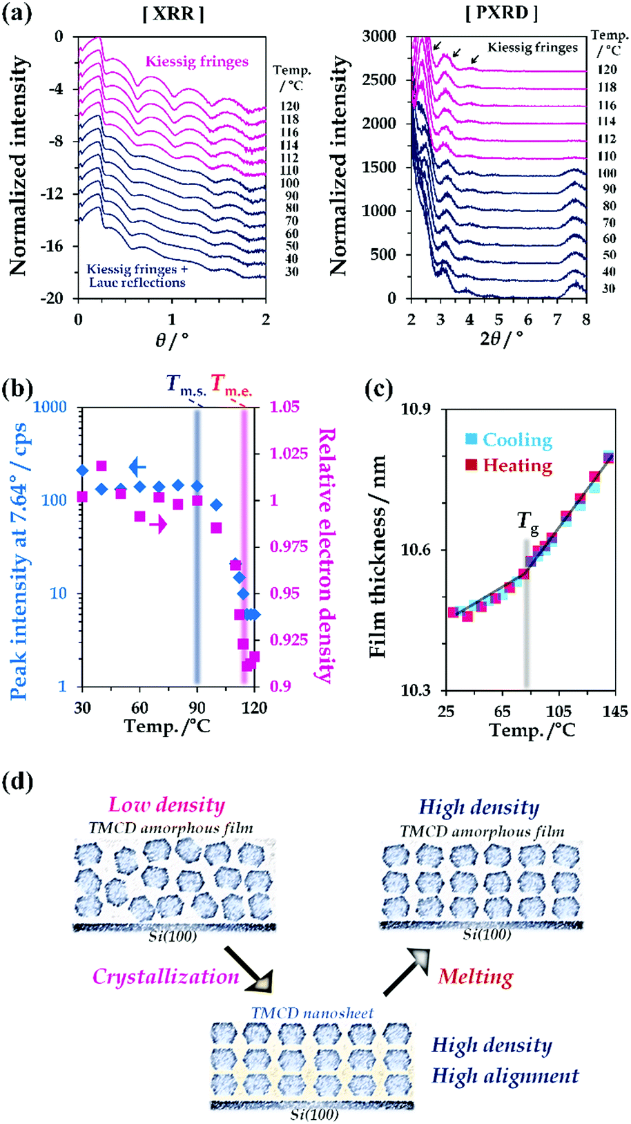 | ||
| Fig. 3 (a) Temperature-dependent XRR and PXRD profiles for TMCD films; initial film is TMCD crystalline nanosheet. (b) Peak intensity at 7.64° and relative electron density as a function of temperature. Here, electron density at 90 °C was used as unity. Tm.s. and Tm.e. indicate the start and end temperatures. (c) Thickness change of TMCD amorphous film prepared via melting of TMCD nanosheets in the cooling and subsequent heating processes. (d) Schematic of the proposed TMCD melting via melting of nanosheet crystals, in which the TMCD molecules are perpendicularly ordered. | ||
In the initial state, in addition to several Kiessig fringes, fringes from the Laue reflection developed in the XRR profile of the nanosheet crystals [Fig. 3(a), left]. As the temperature increases above 90 °C, the peak intensity gradually decreases, indicating the onset of melting. This terminates around 120 °C. Note that the 2θ/ω profiles of the TMCD melt film still exhibit clear Kiessig fringes in the XRR profiles without the Laue reflection, showing the persistence of the flatness in the TMCD amorphous film after the nanosheet crystals melt.
Fig. 3(b) plots the results of the relative electron density of the TMCD film as a function of temperature in addition to the peak intensity at 7.64°. The decreased electron density obtained by fitting the XRR profile in the low-angle range clearly shows a good correlation with the decrease of the peak intensity. In other words, the electron density decreases in the melting process, following thermodynamic behaviour. The electron density of the crystal is generally greater than the melt due to the rapid increase in volume in the melt.60
Meanwhile, in our previous work,45 an irreversible thickness change was observed for a TMCD melt film during the heating and cooling processes because of the anomalous continuous decrease in the film thickness above Tg. However, in this study, for the TMCD amorphous film prepared by melting the TMCD nanosheets, a reversible thickness change was discernible in the cooling and subsequent heating processes [Fig. 3(c)]. The reason is believed to be as follows: because the nanosheets have a highly ordered crystalline structure, the corresponding melt must possess a denser structure than the spin-coated film. Furthermore, the stable molecular assembly formed via nanosheet crystal formation may drastically reduce the rearrangement of TMCD molecules, which might be the driving force to reduce the film thickness in our previous work. As a result, the melting of a highly ordered nanosheet crystal can yield a more stable amorphous film that did not exhibit the anomalous decrease of the film thickness above Tg. This film should be usable to study the glass transition behaviour. Actually, from Fig. 3(c), Tg can therefore be determined as the intersection of two extrapolated lines, indicating Tg = 83.5 °C from the different thermal expansion properties of the thicknesses.
Hierarchical structure in thicker films
Fig. 4(a) shows the 2D-GIXD profiles for a thicker TMCD film (ca. 59 nm) before and after thermal annealing. The 2D-GIXD profile for the TMCD film before thermal annealing [Fig. 4(a), top] shows a ring-shape halo-like reflection with a d spacing of 7.9 Å. This broad reflection indicates the amorphous state of TMCD; several broad diffractions are intrinsic characteristics of amorphous TMCD.39–42 Conversely, after thermal annealing, several reflections with d spacings of 10.7, 7.5 and 5.0 Å with relatively wide azimuthal ranges appear in both the out-of-plane (meridional) and in-plane (equatorial) directions, whereas no reflections are discernible in the other directions [Fig. 4(a), bottom]. This indicates that the structure is aligned but disordered. In addition, no reflections from the (110) plane appear, as observed for TMCD crystalline nanosheets with ca. 12 nm film thickness, demonstrating clearly that the molecular assembly behaviour differs distinctly. Summarising the results of the XRR, PXRD and 2D-GIXD profiles, the hierarchical structure in the thicker film is expected to evolve as follows: (i) the lack of Kiessig fringes in the XRR profile indicates an inhomogeneous state, such as a dewetted or agglomerated state. (ii) The PXRD and 2D-GIXD results show the formation of a less ordered but somewhat aligned structure. Thus, at least, no possibility of a flat nanosheet structure is assumed. Conversely, the observed 2D-GIXD profiles are similar to those reported for helical fibrous crystals formed by peptide fragments,61 amyloid fibrils,62 insulin fibrils,63 synthetic polymers with helical structures,64etc. Thus, we deduce that a helical molecular assembly structure forms. To check the structure in the thicker TMCD film, we used AFM. | ||
| Fig. 4 Characterisation of the thick TMCD film with ca. 59 nm initial film thickness. (a) 2D-GIXD profiles before and after thermal annealing at 120 °C for 24 h. (b) AFM image obtained for the TMCD film after thermal annealing. | ||
In the AFM image, the film morphology is inhomogeneous, as expected, and sophisticated nano-fibrous structures are recognised [Fig. 4(b)]. The nanofibre structure has periodic irregularities with approx. 260 nm periods on the flat Si substrate [Fig. 4(b), right]. At many locations, nanofibres are bundled, and dewetting domains appear in many areas.
To support the above observations, field-emission-SEM measurements were made in both SE1 and SE2 modes. SE1 mode mostly detects secondary electrons mainly emitted from the surface. Because the fraction of secondary electrons emitted from the surface shows an angular distribution on the detector, SE1 mode can give information on the surface. Conversely, SE2 mode detects not only secondary electrons but also backscattered electrons and gives information on the bulk.
Fig. 5 shows the FE-SEM images of the TMCD films (ca. 59 nm) annealed for 0 [Fig. 5(a)], 3 [Fig. 5(b)] and 36 h [Fig. 5(c)–(g)], respectively. In Fig. 5, the left SEM image (l) and Fig. 5(f) and (g) show the images obtained in SE1 mode, whereas the right (r) image was obtained in SE2 mode. In the left SEM images, the white domains in the images show the dewetted domain; the fraction of secondary electrons is strong from the Si substrate because of its smooth surface, whereas the other black areas indicate that TMCD is well covered, similar to the initial state [0 h, Fig. 5(a)]; this supports the conclusions from the AFM images. Also, the formation of nanofibre structures is clearly recognised in the SEM images. Fig. 5(b) depicts the smallest fibre domain that we could observe. It indicates that both agglomeration of nanofibres and dewetting cooperatively occurred, which indicates that the dewetting is likely to occur when the fibre domain is agglomerated. For the SEM image obtained for the TMCD film after thermal annealing for 36 h, the full area is occupied by the fibrous architecture. Some nanofibres are well rounded and do not seem to be in solid crystalline form, as observed for polylactide crystals developed in ultrathin films.33
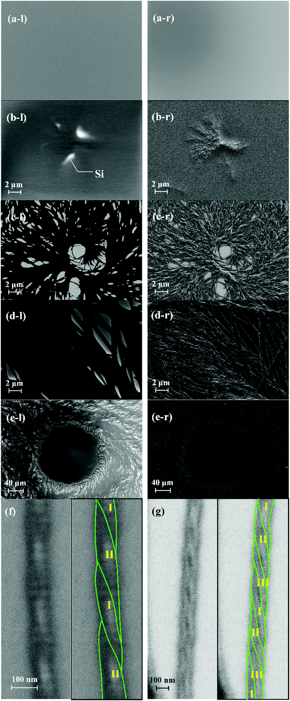 | ||
| Fig. 5 SEM images for TMCD films (ca. 59 nm) after thermal annealing for (a) 0 h, (b) 3 h and (c–g) 36 h. The left images of (a–e) were obtained using SE1 mode, while the right images of (a–e) were taken in SE2 mode. In panels (f and g), where SE2 mode was used, the raw image (left) and the image in which the constituted fibres in the non-bundled nanofibres are numbered with roman numerals (right). | ||
Fortunately, we could observe well-grown fibrous domains without the bundled state [Fig. 5(f) and (g)] and found that some fibres contained double helix and triple helix structures. Here, the width increases as the number of fibres increases; the double helix is ca. 100 nm wide, while the triple helix is ca. 150 nm wide. However, the pitch length is ca. 250 nm for both cases, suggesting that one fibre is 50 nm wide. The pitch length agrees with that observed in the AFM images [Fig. 4(b)]. In addition to the observation of rounded nanofibres, these observations fully explain the insights that the evolved architectures in the thicker film must be less ordered with highly frustrated energy. Possibly to reduce the frustrated energy of the single-nanofibre state, attraction or entanglement between each nanofibre occurs, which leads to agglomeration. These helical nanofibre structures must consist of semicrystalline structures with both ordered and disordered domains, which may consist of helical structures.
Discussion of the self-organisation factor of the nanofibre structure
The surface and/or interfacial roughness leads to a different type of hierarchical structure. In a previous study, we reported how the solvent used for spin-coating leads to different interfacial roughnesses.45 The surface roughness of the spin-coated TMCD amorphous film prepared using ethanol is apparently much greater than that using chloroform. In this case, however, we observed similar crystallisation behaviour for both the nanosheet and nanofibre forms depending on the film thickness (data not shown). However, we further examined the crystallisation behaviour of the TMCD film with a roughened surface prepared by mechanical grinding using a cotton stick. We observed no significant difference in the thinner film that formed nanosheets (data not shown), whereas a distinct change for the thicker film, which typically forms nanofibre structures, was observed in the 2D-GIXD profile (Fig. 6(a)). For the 2D-GIXD profile of the TMCD film prepared by mechanical rubbing, there are many clear reflections with wide azimuth ranges and a ring-like shape with d spacings of 15.5, 12.9, 11.7, 10.9, 10.6, 9.1, 8.8, 8.1, 8.0, 7.5 Å, etc. These reflections can be assigned as the (011), (101), (110), (012), (111), (021), (112), (120), (013), and (103) reflections, respectively, of the monohydrate TMCD crystal.44 The SEM image of the TMCD film shows a broken leaf-like morphology; characteristics of both the nanofibres and nanosheets seem to exist, which differs significantly from the images obtained for the thermal-annealed TMCD films without rubbing.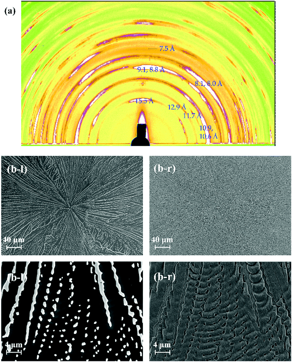 | ||
| Fig. 6 (a) 2D-GIXD profile and (b) SEM images of the TMCD film (ca. 121 nm) which was obtained after thermal annealing of the rubbed TMCD film. | ||
We also considered how the solvent affects the nanofibre structure. In the previous study related to polymer-free nanofibres, it was necessary to use solvent for the electrospinning technique and no helical structure appeared. However, we obtained helical nanofibres without using solvent in the self-organisation process; thus, the present solvent may be an important parameter to determine whether the helical nanofibres form. Because TMCD dissolves readily in organic solvent and water, the effects of solvent were checked by vapouring the organic solvent. Fig. 7(a) and (b) show SEM and AFM images, respectively, for the TMCD film after ethanol vapouring for 10 min. Apparently, no helical nanofibre structure remains after vapouring; instead, a nanoarchitecture with high crystallinity develops. Recrystallisation or transformation of the helical nanofibres with a greatly frustrated structure to a thermodynamically stable crystalline solid appeared to occur. This result strongly suggests that the solvent readily assists the transformation from an unstable to a stable form; this explains why the use of solvent often prevents the formation of a frustrated architecture, such as helical nanofibres consisting of TMCD, which exhibit a high susceptibility to the solvent.
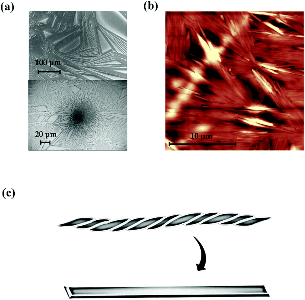 | ||
| Fig. 7 (a) SEM and (b) AFM images of the TMCD film (ca. 59 nm) after vapouring of ethanol for 10 min. (c) Schematic of the recrystallisation from nanofibres to a crystalline stick. | ||
Finally, we discuss the formation mechanism of the helical nanofibre structure in the nano-films with thicknesses above ca. 59 nm. To date, several deformation mechanisms have been proposed, such as surface stress, surface and space charges, the Eshelby twist and heterometry stress.22 Unfortunately, reaching a conclusion relating to the formation of helical nanofibres for TMCD is difficult at this stage. Considering the single-crystal formation in the nanosheets, the formation of single-crystal growth in one direction may be the driving force to develop the fibre structure. From the results of the experiment using mechanical rubbing, we assumed that crystallisation in the homogeneous film is important to prolong surface stress or to neutralize the surface charges of TMCD, whereas small differences in interfacial roughness do not appear to induce the critical determination. Solvent vapouring must be prevented to prevent recrystallization of the unstable architecture. However, we deem that even if these conditions are satisfied, whether this phenomenon occurs for the other CDs is obscure. The unique properties of TMCD bulk crystals and the TMCD molecule have been extensively reported. TMCD bulk crystals appear to have less crystallinity, suggesting an unstable solid.42 In another report, TMCD was reported to exhibit a unique transformation characteristic in its sugar where one sugar unit changes its structure from 4C1 to 1C4 in the CD molecule for the monohydrate crystal form.43 These unique characteristics can yield an adaptive interface to connect to frustrated structures, such as helical nanofibers, by reducing the interfacial energy or stabilising the intermolecular network. The uniqueness of TMCD crystals may determine the formation of the helical nanofibre structure, whereas other CD crystals can also provide similar properties. However, as far as we know, no similar results have been reported.
Conversely, several CDs have been reported to form aggregates, which enables the fabrication of polymer-free CD non-helical amorphous nanofibres.11,12 Therefore, there is a possibility that those CD aggregates assemble into helical fibrils, as proposed for insulin oligomers.65 To answer these questions, further exploration of the polymer-free hierarchical CD nanostructuring is necessary. Because the formation of helical nanofibres must rely on intrinsic mechanical properties such as deforming, in addition to the optical properties of the formed inclusion complexes, helical CD nanofibres without organic inclusions may have interesting applications.
Conclusions
In ultrathin films, we developed nanosheets and helical nanofibres consisting of TMCD without adding polymeric carriers and without using organic solvents or vapour. Also, we ensured the correlation between the results of the X-ray analyses and microscopic observations and showed that XRR can be a powerful tool to analyse not only noncrystalline films but also crystalline films. PXRD and 2D-GIXD analyses were also useful, as summarised in Table 1. Because the prepared hierarchical nanostructures contain CDs without inclusion complexes, these hierarchical architectures may exhibit sophisticated functionality by exploiting their unique properties. Also, without inclusion, the unique mechanical characteristics of the TMCD crystals, which enable them to frustrate (helically deform), may open the possibility of using them as mechanical sensors. As far as we know, this is the first example of the use of a cyclodextrin without modification by ‘sophisticated’ substitutes to form helical nanofibres without polymeric species or organic inclusion complexes.| Method | Thinner film (ca. 12 nm) | Thicker film (ca. 121 nm, 243 nm) |
|---|---|---|
| The middle thickness film (ca. 59 nm) was confirmed to be a mixture of nanosheets and nanofibres by X-ray analyses. | ||
| XRR | Clear Kiessig fringes (roughness of film must be small) | No fringe (roughness of film must be large) |
| PXRD | Sharp diffraction peak (ordering structure) | Unclear diffraction peak (non-ordered structure in the measured axis) |
| GIXD | Spotty reflections (highly oriented crystalline structure) | Broad reflection in the azimuth direction with orthogonal locations (less ordered structure or helical structure) |
| AFM | Nanosheets | Nanofibres |
| SEM | — | Helical nanofibres |
Conflicts of interest
There are no conflicts to declare.Acknowledgements
We are grateful for the fruitful discussion with Professor Satoru Kato, Kwansei Gakuin University, Japan. This work was financially supported by the Amano Institute of Technology, AIST, Japan, by the MEXT-Supported Program for the Strategic Research Foundation at Private Universities (S1201027) 2012–2016, by the Japan Society for the Promotion of Science (Grant-in-Aid for Scientific Research (C) 24560033) and by the Japan Society for the Promotion of Science (Grant-in-Aid for Scientific Research (C) 24560033, 17K05617). The synchrotron radiation experiments were performed in the first hutch of BL03XU, SPring-8, as constructed by the Consortium of Advanced Soft material Beamline (FSBL) with the approval of the JASRI (Proposal no. 2015A7204 & 2015B7254).References
- A. Harada, J. Li and M. Kamachi, Nature, 1992, 356, 325–327 CrossRef.
- K. A. Conners, Chem. Rev., 1997, 997, 1325–1357 CrossRef.
- T. Loftsson and M. E. Brewster, J. Pharm. Sci., 1996, 85, 1017–1025 CrossRef PubMed.
- G. Li and L. B. McGown, Science, 1994, 264, 249–251 CrossRef PubMed.
- A. E. Tonelli, Polymer, 2008, 49, 1725–1736 CrossRef.
- Y. He, P. Fu., X. Shen and H. Gao, Micron, 2008, 39, 495–516 CrossRef PubMed.
- N. Rajendiran, G. Venkatesh and J. Saravanan, Spectrochim. Acta, Part A, 2014, 129, 157–162 CrossRef PubMed.
- G. Narayanan, R. Boy, B. S. Gupta and A. E. Tonelli, in Polysaccharide-based Fibers and Composites, ed. L. Lucia and A. Ayoub, Springer International Publishing, 2018, ch. 3, pp. 29–62 Search PubMed.
- A. Celebioglu and T. Uyar, Chem. Commun., 2010, 46, 6903–6905 RSC.
- A. Celebioglu and T. Uyar, Langmuir, 2011, 27, 6218–6226 CrossRef PubMed.
- A. Celebioglu and T. Uyar, Nanoscale, 2012, 4, 621–631 RSC.
- W. Zhang, M. Chen, B. Zha and G. Diao, Phys. Chem. Chem. Phys., 2012, 14, 9729–9737 RSC.
- J. L. Manasco, C. D. Saquing, C. Tang and S. A. Khan, RSC Adv., 2012, 2, 3778–3784 RSC.
- A. Celebioglu and T. Uyar, RSC Adv., 2013, 3, 22891–22895 RSC.
- A. Celebioglu and T. Uyar, J. Colloid Interface Sci., 2013, 404, 1–7 CrossRef PubMed.
- A. Celebioglu, F. Kayaci-Senirmak, S. I. Kusku, E. Durgun and T. Uyar, Food Funct., 2016, 7, 3141–3153 RSC.
- A. Celebiolglu, H. S. Sen, E. Durgun and T. Uyar, Chemosphere, 2016, 144, 736–744 CrossRef PubMed.
- A. Celebioglu, S. Vempati, C. Ozgit-Akgun, N. Biyikli and T. Uyar, RSC Adv., 2014, 4, 61698–61705 RSC.
- A. Celebiolgu and T. Uyar, RSC Adv., 2013, 3, 10197–10201 RSC.
- Y. Wang, J. Xu, Y. Wang and H. Chen, Chem. Soc. Rev., 2013, 42, 2930–2962 RSC.
- A. Sorrenti, O. Illa and R. M. Ortuño, Chem. Soc. Rev., 2013, 42, 8200–8219 RSC.
- A. G. Shtukenberg, Y. O. Punin and A. G. B. Kahr, Angew. Chem., Int. Ed., 2014, 53, 672–699 CrossRef PubMed.
- L. Liu, L. Zhang, S. M. Kim and S. Park, Nanoscale, 2014, 6, 935–9365 Search PubMed.
- M. Liu, L. Zhang and T. Wang, Chem. Rev., 2015, 115, 7304–7397 CrossRef PubMed.
- B. Lotz and S. Z. D. Cheng, Polymer, 2005, 46, 577–610 CrossRef.
- C. Y. Li, S. Z. D. Cheng, J. J. Ge, F. Bai, J. Z. Zhang, I. K. Mann and F. W. Harris, Phys. Rev. Lett., 1999, 83, 4558–4561 CrossRef.
- C. Y. Li, D. Yan, S. Z. D. Cheng, F. Bai, T. He, L.-C. Chien, F. W. Harris and B. Lotz, Macromolecules, 1999, 32, 524–527 CrossRef.
- R.-M. Ho, Macromolecules, 2000, 33, 7529–7537 CrossRef.
- C. Y. Li, J. J. Ge, F. Bai, B. H. Calhoun, F. W. Harris and S. Z. D. Cheng, Macromolecules, 2001, 34, 3634–3641 CrossRef.
- C. Y. Li, S. Z. D. Cheng, X. Weng, J. J. Ge, F. Bai, J. Z. Zhang, B. H. Calhoun, F. W. Harris, L.-C. Chien and B. Lotz, J. Am. Chem. Soc., 2001, 123, 2462–2463 CrossRef PubMed.
- C. Y. Li, S. Jin, X. Weng, J. J. Ge, D. Zhang, F. Bai, F. W. Harris and S. Z. D. Cheng, Macromolecules, 2002, 35, 5475–5482 CrossRef.
- H. Schönherr and C. W. Frank, Macromolecules, 2003, 36, 1199–1208 CrossRef.
- D. Maillard and R. E. Prud’homme, Macromolecules, 2008, 41, 1705–1712 CrossRef.
- Y.-X. Liu and E.-Q. Chen, Coord. Chem. Rev., 2010, 254, 1011–1037 CrossRef.
- B. Crist and J. M. Schultz, Prog. Polym. Sci., 2015, 56, 1–63 CrossRef.
- T. Carofiglio, R. Fornasier, V. Lucchini, C. Rosso and U. Tonellato, Tetraheron Lett., 1996, 37, 8019–8022 CrossRef.
- K. Kano, R. Nishiyabu, T. Asada and Y. Kuroda, J. Am. Chem. Soc., 2002, 124, 9937–9944 CrossRef PubMed.
- Y. Tsuchiya, T. Shiraki, T. Matsumoto, K. Sugikawa, K. Sada, A. Yamano and S. Shinkai, Chem. – Eur. J., 2012, 18, 456–465 CrossRef PubMed.
- I. Tsukushi, O. Yamamuro and H. Suga, J. Therm. Anal., 1991, 37, 1359 CrossRef.
- I. Tsukushi, O. Yamamuro and H. Suga, J. Therm. Anal., 1995, 45, 905–915 CrossRef.
- M. Makita, Y. Yoshihashi, E. Fukuoka and K. Terada, Chem. Pharm. Bull., 1998, 46, 822–825 CrossRef.
- I. Tsukushi, T. Kanaya, O. Yamamuro, T. Matsuo and K. Kaji, J. Phys. Chem. Solids, 1999, 60, 1545–1547 CrossRef.
- M. R. Caira, V. J. Griffith, L. R. Nassimbeni and B. van Oudtshoorn, J. Chem. Soc., Perkin Trans. 2, 1994, 2071–2072 RSC.
- M. R. Caira, S. A. Bourne, W. T. Mhlongo and P. M. Dean, Chem. Commun., 2004, 2216–2217 RSC.
- S. Ogawa and I. Takahashi, Cryotech. Cryobiol., 2018, 64, 19–27 Search PubMed.
- J. L. Keddi, R. A. L. Jones and R. A. Cory, Europhys. Lett., 1994, 27, 59–64 CrossRef.
- C. Yang and I. Takahashi, Polym. J., 2011, 43, 390–397 CrossRef.
- R. R. Baglay and C. B. Roth, J. Chem. Phys., 2017, 146, 203307 CrossRef PubMed.
- M. Tolan, Springer Tracts in Modern Physics. X-Ray Scattering from Soft-Matter Thin Films, Materials Science and Basic Research, Spriner, Berlin, vol. 148, 1999 Search PubMed.
- M. Yasaka, X-ray thin-film measurement techniques V. X-ray reflectivity measurement, Rigaku J., 2010, 26, 1–9 Search PubMed.
- S. Ogawa and I. Takahashi, In Carbohydrate, ed. Caliskan M., Kavakli H. and Öz G., InTech, 2017, pp. 115–130 Search PubMed.
- S. Ogawa and I. Takahashi, Crystals, 2017, 7, 356 CrossRef.
- J. Frank, J. F. Holzwarth and W. Saenger, Langmuir, 2002, 18, 5974–5976 CrossRef.
- H. Ogawa, H. Masunaga, S. Sasaki, S. Goto, T. Tanaka, T. Seike, S. Takahashi, K. Takeshita, N. Nariyama, H. Ohashi, T. Ohata, Y. Furukawa, T. Matsushita, Y. Ishizawa, N. Yagi, M. Takata, H. Kitamura, A. Takahara, K. Sakurai, K. Tashiro, T. Kanaya, Y. Amamiya, K. Horie, M. Takenaka, H. Jinnai, H. Okuda, I. Akiba, I. Takahashi, K. Yamamoto, M. Hikosaka, S. Sakurai, Y. Shinohara, Y. Sugihara and A. Okada, Polym. J., 2013, 45, 109–116 CrossRef.
- A. L. Patterson, Phys. Rev., 1939, 56, 978–982 CrossRef.
- A. P. Hammersley, J. Appl. Crystallogr., 2016, 49, 646–652 CrossRef.
- M. Hara, H. Sasabe, A. Yamada and A. F. Garito, Jpn. J. Appl. Phys., 1989, 28, L306–L308 CrossRef.
- S. Ogawa, Y. Ozaki and I. Takahashi, ChemPhysChem, 2016, 17, 2808–2812 CrossRef PubMed.
- J. I. Langford and A. J. C. Wilson, J. Appl. Crystallogr., 1978, 11, 102–113 CrossRef.
- W. Kauzmann, Chem. Rev., 1948, 43, 219–256 CrossRef.
- P. Sikkorski, E. D. T. Atkins and L. C. Serpell, Structure, 2003, 11, 915–926 CrossRef.
- J. E. Gillam and C. E. MacPhee, J. Phys.: Condens. Matter, 2013, 25, 373101 CrossRef PubMed.
- M. I. Ivanova, S. A. Sievers, M. R. Sawaya, J. S. Wall and D. Eisenberg, Proc. Natl. Acad. Sci. U. S. A., 2009, 106, 18990–18995 CrossRef PubMed.
- Y. Hase, K. Nagai, H. Iida, K. Maeda, N. Ochi, K. Sawabe, K. Sakajiri, K. Okoshi and E. Yashima, J. Am. Chem. Soc., 2009, 131, 10719–10732 CrossRef PubMed.
- B. Vestergaard, M. Groenning, M. Roessle, J. S. Kastrup, M. van de Weert, J. M. Flink, S. Frokjaer, M. Gajhed and D. I. Svergun, PLoS Biol., 2007, 5, 1089–1097 CrossRef PubMed.
Footnote |
| † Electronic supplementary information (ESI) available. See DOI: 10.1039/c8qm00299a |
| This journal is © the Partner Organisations 2018 |