
Processing and manufacturing of graphene-based microsupercapacitors
Guofeng
Zhang
,
Yuyang
Han
,
Changxiang
Shao
,
Nan
Chen
 *,
Guoqiang
Sun
,
Xuting
Jin
,
Jian
Gao
,
Bingxue
Ji
,
Hongsheng
Yang
and
Liangti
Qu
*
*,
Guoqiang
Sun
,
Xuting
Jin
,
Jian
Gao
,
Bingxue
Ji
,
Hongsheng
Yang
and
Liangti
Qu
*
Key Laboratory of Photoelectronic/Electrophotonic Conversion Materials, Key Laboratory of Cluster Science, Ministry of Education of China, School of Chemistry and Chemical Engineering, Beijing Institute of Technology, Beijing 100081, P. R. China. E-mail: gabechain@bit.edu.cn; lqu@bit.edu.cn
First published on 13th July 2018
Abstract
Portable electronic devices and electric vehicles have greatly stimulated the development of micro-sized energy storage devices. Electrochemical capacitors, which have the abilities of rapid charge and discharge, high energy storage and outstanding cyclic stability, can bridge the gap between batteries and conventional electrolytic capacitors. Graphene, an emerging two-dimensional (2D) material, is an excellent choice to fabricate electrodes. With the abovementioned abilities, graphene-based microsupercapacitors (graphene-based MSCs) are promising future energy storage devices to promote the practical application of portable electronics and microelectronic devices. This review aims to summarize the latest developments in graphene-based MSCs and the methods of processing miniature graphene electrodes to provide higher performance. In addition, we are also committed to critically analyzing the status of graphene-based MSCs and, on this basis, forecasting their future challenges, perspectives and opportunities.
 Guofeng Zhang | Guofeng Zhang is currently a master candidate under the supervision of Prof. Liangti Qu and Dr Nan Chen at Beijing Institute of Technology (BIT). His research mainly focuses on graphene based energy storage devices, especially microsupercapacitors. |
 Yuyang Han | Yuyang Han is currently a master candidate under the supervision of Prof. Liangti Qu and Prof. Zhipan Zhang at Beijing Institute of Technology (BIT). Her research mainly focuses on graphene-based moisture-induced power generation and energy storage devices. |
 Nan Chen | Nan Chen received his Bachelor's degree from China Agricultural University in 2006. Then he received a PhD in Chemistry from Institute of Chemistry, Chinese Academy of Sciences (ICCAS, Beijing, China). He is now an associate professor at Beijing Institute of Technology (BIT). His current research interests lie in the development of new methods and strategies for fabrication of carbon-based functional materials for various applications. |
 Liangti Qu | Liangti Qu received a PhD in Chemistry from Tsinghua University (Beijing, China) in 2004. He is now a Professor of Chemistry at the Beijing Institute of Technology and leads the nanocarbon research group. His research interests in materials chemistry mainly focus on the synthesis, functionalization and application of nanomaterials with carbon–carbon conjugated structures, including carbon nanotubes, graphene and conducting polymers. |
1 Introduction
With the development of technology, greater requirements for electronic devices have arisen. Small-scale micropower and energy storage units are widely used in home automation, transport surveillance, health control, environmental monitoring and industrial processes tracking.1,2 Today, almost all markets use energy storage device batteries as commercial micropower electronic devices to produce electricity. However, certain characteristics of batteries, such as environmental pollution, limit their applications. Supercapacitors (SCs), also called electrochemical capacitors or ultracapacitors, are playing increasingly important roles and may even replace batteries in many applications.3,4 SCs usually have higher power densities as well as the abilities of rapid charge/discharge cycling and long cycling life.5–7 However, ordinary SCs have low energy densities, which is a major issue that must be urgently addressed; also, the electrode materials of conventional SCs have smaller specific surface areas than those of SCs-based graphene materials, resulting in smaller capacitance. Since graphene was first isolated in 2004, researchers have found that it has a 2D structure with single atomic thickness and a large surface area.8,9 Due to the unique properties of graphene, it is favourable for applications in energy conversion, energy storage, etc.10–32 In particular, graphene-based materials have attracted great interest for the fabrication of SC electrodes because their specific surface areas can reach 2630 m2 g−1. Recently, it was reported that the maximum theoretical specific capacitance of single layer graphene can achieve 21 μF cm−2; this is the highest value of graphene-based materials applied to electrochemical double layer capacitors.48 Furthermore, graphene-based electrode materials have many excellent characteristics, such as flexibility, transparency, miniaturization and ultrathinness; these can be adapted for more applications, which is the main trend of the future. Interestingly, the ability of graphene-based electrode materials to enable electrolyte ions to interact rapidly with electrode material layers in the horizontal direction is superior to those of conventional materials.33,34 It is reported that the process of graphene dispersion into electrodes can be achieved by various methods, such as dip coating, rod coating, and spray coating.35,36 Graphene-based MSCs are mainly used in portable, wearable and flexible electronic devices.34,37–40 Although research on graphene-based MSCs has made great progress in this area, it is urgent to enhance the performance of MSCs and realize their applications in daily life.A conventional sandwich structure SC contains electrodes, current collectors, electrolytes, and separators. Each component has a significant impact on its electrochemical and mechanical properties. As we know, although the separator prevents shorting of the two electrodes of the SC, it hinders the movement of ions in the electrolyte and severely limits the mechanical properties of the SC. Therefore, when studying the first three influencing factors, it is also necessary to study the equipment configuration of the SC. In order to avoid the use of splitters, a new architecture configuration of the MSC has been proved to be a good choice. There is no clear definition of an MSC in the previous literature; however, as the name suggests, an MSC should be a thinner and smaller SC. They should be designed to supply power to microelectronics as micropower sources. Typically, the footprint of the MSC should be in centimeters, millimeters or less. If categorized by dimensions, the MSC can be divided into one-dimensional (1D), 2D, three-dimensional (3D) and sandwich MSCs. 1D MSCs are mainly present in the form of fibers, including positive and negative fiber electrodes and all solid electrolytes. 2D and 3D MSCs exist in the form of planar micro-fingers; they mainly include electrodes, current collectors and electrolytes. Compared to a conventional interlayer SC, this design not only imparts a high edge-to-area ratio to the electrode, but also shortens the distance along which ions diffuse between two adjacent electrodes. This increases the usable area of the electrode material and promotes ion diffusion of the electrolyte.
In summary, compared with traditional SC electrode materials, graphene-based MSC electrode materials achieve higher electrical conductivity and richer hierarchical structures. Based on these excellent features, graphene has been considered to be one of the most suitable alternative materials for MSCs in recent years.
2 Processing and manufacturing of graphene-based MSCs
There are many methods to manufacture graphene-based MSCs with different morphology dimensions. Current methods of micro-machining of graphene-based MSCs mainly comprise hydrothermal methods, wet-spin methods, laser engraving technology, O2 plasma treatment, photolithography techniques, printing techniques, electrochemical deposition techniques, etc. 1D graphene-based MSCs are obtained using hydrothermal methods, while 2D and 3D MSCs are processed by print technology. On the one hand, the processing methods will determine the precision of the electrodes of graphene-based MSCs, which is a crucial factor for the architecture of graphene-based MSCs. On the other hand, the architecture of MSCs plays a pivotal role in the performance of the MSCs. Therefore, it is necessary to choose a suitable processing method to build graphene-based MSCs to improve their electrochemical performance and their potential application in daily life. For MSCs, the choice of processing method should be based on a combination of their processing dimensions, materials, and accuracy. Here, we summarize the general characteristics of the treatment of graphene-based MSCs in Table 1. The treatment of graphene MSCs has an important influence on their electrochemical performance. It is well known that in MSCs, in addition to electrodes, current collectors and electrolytes, the influence of the MSC structure on its electrochemical performance is a factor that cannot be ignored. The treatment method directly determines the structure of the MSC. In many cases, these processing methods can be replaced with each other. For example, both focused ion beams and lasers can be used to simultaneously reduce and pattern GO. However, the patterns processed by the former have higher precision. In other cases, the processing method cannot be directly replaced. If only oxygen can be used to pattern GO, further reduction of the GO is needed.| Processing method | Dimension | Advantages | Disadvantages | Scale | Cost | Ref. |
|---|---|---|---|---|---|---|
| Hydrothermal | 1D | Continuous production | High temperature | Large | Medium | 40 |
| High pressure | ||||||
| Wet-spin | 1D | Low temperature | Chemical reduction reagent assistance | Medium | Low | 44 |
| Laser technology | 1D/2D/3D | Processing in multiple dimensions | High temperature-resistant substrates | Medium | Low | 38, 49 and 65 |
| No mask | Low precision processing submicron patterns | |||||
| Printing technology | 2D/3D | Processing on various substrates | Inkjet nozzles are prone to clogging | Large | Low | 75 and 79 |
| Makes full use of active materials | ||||||
| Oxygen plasma treatment | 2D | Reliable | Insufficient use of active materials | Medium | Medium | 39 |
| Short time | Mask-assisted | |||||
| Photolithography | 2D | Simple | Insufficient use of active materials | Medium | Low | 96 |
| Ultrafine micro/nanopatterning | Mask-assisted | |||||
| Electrochemical deposition | 2D | Simple process to obtain asymmetric MSCs | Processing on conductive substrates | Small | Medium | 102 |
| Various substrates | ||||||
| Press-assisted template method | 2D | Simple | Mask-assisted | Large | Low | 103 |
| High efficiency | ||||||
| Focused ion beams | 2D | High precision processing submicron patterns | Insufficient use of active materials | Medium | Low | 104 |
| Photoreduction | 2D | Easy to achieve various patterns | Titanium dioxide-assisted | Large | Low | 105 |
| Pen lithography | 2D | Simple | Low precision | Small | Low | 106 |
| Vacuum filtration | 2D | Very simple | Slow processing | Small | Low | 107 |
| Various substrates | Mask-assisted | |||||
| Thermal decomposition | Sandwich structure | Strong adhesion in active materials and substrates | High temperature | Small | Medium | 110 |
2.1 Hydrothermal method
1D graphene-based MSCs not only encompass flexibility and facile weaving properties, but also integrate the advantages of the high specific surface area and high conductivity of graphene; therefore, much research interest is focused on the processing of 1D graphene-based MSCs.The hydrothermal method is a common method for synthesizing graphene-based fibers. Graphene oxide and a composite solution thereof are formed by a capillary column and then subjected to high-temperature reduction treatment; finally, a graphene composite fiber is obtained. Using a hydrothermal method, Qu's group synthesized graphene fibers with diameters of about 30 μm and obtained all-graphene core-sheath microfibers by further electrodeposition of graphene on their surfaces.41 The assembled MSC was very flexible and easy to weave. Meanwhile, as reported by Chen and coworkers, a solution of ethylenediamine (EDA) mixed with single-walled carbon nanotubes (SWNTs) and graphene oxide (GO) was subjected to a hydrothermal process to obtain fibers with a high specific surface area (396 m2 g−1) and electrical conductivity (102 S cm−1) (Fig. 1a and b).40 Nitrogen-doped reduced graphene oxide (N-doped RGO)/SWNTs MSCs using polyvinyl alcohol (PVA)/H3PO4 gel as the electrolyte showed a volumetric capacitance up to 45.0 F cm−3 at a low current density of 26.7 mA cm−3 (area capacitance of ∼116.3 mF cm−2). Moreover, the MSCs could retain 93% and 97% of their initial capacitance after 10![[thin space (1/6-em)]](https://www.rsc.org/images/entities/char_2009.gif) 000 charge/discharge cycles and bending 1000 times at 90°, indicating their electrochemical and mechanical stability. Their superior electrochemical and mechanical properties can be mainly attributed to the following reasons: firstly, EDA can be combined with SWNTs and GO to construct a vertically aligned, three-dimensional columnar SWNT/RGO framework. At the same time, the introduction of nitrogen increases the wettability of the heteroatom doping, the conductivity and the tantalum capacitance. Secondly, the combination of graphene oxide and SWNTs exerts a synergistic effect on their mechanical and electrochemical stability, in which the GO shows good dispersion on the SWNTs; also, the SWNTs hinder the restacking of GO sheets. Chen et al. realized the preparation of high-performance fiber-MSCs by a hydrothermal method. The fibers prepared by this method had a large surface area (388.6 m2 g−1), high conductivity, and uniform porous structure.42 Specifically, this all-solid-state fiber-MSC could produce a high capacitance of 1132 mF cm−2 with PVA/H3PO4 gel electrolyte at 0.1 mA cm−2, which is much better than the that of carbon fiber-based MSCs. In addition, when the area power density ranged from 1.5 to 15 W cm−2, the area energy density of the MSC ranged from 95.7 to 46.9 μW h cm−2. The asymmetric MSC even exhibited a higher potential window and energy density compared to the symmetric MSC. The hydrothermal method is considered to be a promising manufacturing method because it can effectively produce asymmetrical MSCs which combine capacitor-type electrode materials as a power source with battery-type faradic electrode materials as an energy source. For example, Chen et al. fabricated asymmetric MSCs consisting of two equal-length electrodes, consisting of RGO/SWNT@MnO2 and nitrogen-doped RGO/SWNT fibers, by a hydrothermal method; the voltage window of the MSCs could be widened to 0 to 1.8 V.43 The resulting MSCs retained 87% of their original capacitance after 10000 charge/discharge cycles at 200 mA cm−3. Remarkably, the MSCs exhibited a higher volumetric energy density of ∼5 mW h cm−3 and a power density of 929 mW cm−3 that was comparable or even superior to that of lithium thin-film batteries (4 V/500 μA h).
000 charge/discharge cycles and bending 1000 times at 90°, indicating their electrochemical and mechanical stability. Their superior electrochemical and mechanical properties can be mainly attributed to the following reasons: firstly, EDA can be combined with SWNTs and GO to construct a vertically aligned, three-dimensional columnar SWNT/RGO framework. At the same time, the introduction of nitrogen increases the wettability of the heteroatom doping, the conductivity and the tantalum capacitance. Secondly, the combination of graphene oxide and SWNTs exerts a synergistic effect on their mechanical and electrochemical stability, in which the GO shows good dispersion on the SWNTs; also, the SWNTs hinder the restacking of GO sheets. Chen et al. realized the preparation of high-performance fiber-MSCs by a hydrothermal method. The fibers prepared by this method had a large surface area (388.6 m2 g−1), high conductivity, and uniform porous structure.42 Specifically, this all-solid-state fiber-MSC could produce a high capacitance of 1132 mF cm−2 with PVA/H3PO4 gel electrolyte at 0.1 mA cm−2, which is much better than the that of carbon fiber-based MSCs. In addition, when the area power density ranged from 1.5 to 15 W cm−2, the area energy density of the MSC ranged from 95.7 to 46.9 μW h cm−2. The asymmetric MSC even exhibited a higher potential window and energy density compared to the symmetric MSC. The hydrothermal method is considered to be a promising manufacturing method because it can effectively produce asymmetrical MSCs which combine capacitor-type electrode materials as a power source with battery-type faradic electrode materials as an energy source. For example, Chen et al. fabricated asymmetric MSCs consisting of two equal-length electrodes, consisting of RGO/SWNT@MnO2 and nitrogen-doped RGO/SWNT fibers, by a hydrothermal method; the voltage window of the MSCs could be widened to 0 to 1.8 V.43 The resulting MSCs retained 87% of their original capacitance after 10000 charge/discharge cycles at 200 mA cm−3. Remarkably, the MSCs exhibited a higher volumetric energy density of ∼5 mW h cm−3 and a power density of 929 mW cm−3 that was comparable or even superior to that of lithium thin-film batteries (4 V/500 μA h).
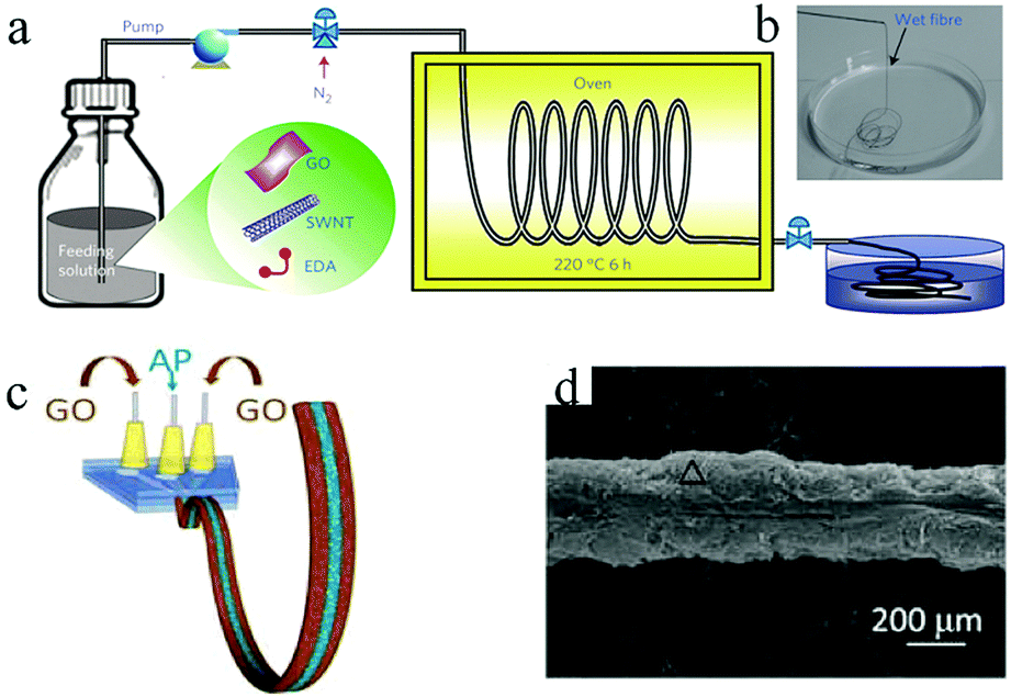 | ||
| Fig. 1 (a) Schematic of the fabrication of SWNT/RGO fibers. (b) Photograph of the obtained SWNT/RGO fiber.40 (Reprinted with permission from Macmillan Publishers Ltd Copyright 2014.) (c) Scheme of the wet-spin process to obtain GO/Aca-PVA/GO fiber. (d) SEM of the freeze-dried GO/Aca-PVA/GO fiber.44 (Reprinted with permission from The Royal Society of Chemistry. Copyright 2016.) | ||
2.2 Wet-spin method
Wet spinning is another effective method for synthesizing graphene fibers, especially for manufacturing one-dimensional graphene-based MSCs. In the wet spinning process, a viscous aqueous solution of graphene oxide and its composite are injected into an aqueous ethanol solution through a microfluidic tube to be solidified. The resulting fibers then require further reduction and drying to obtain graphene and its composites. In this fabrication, the surface porosity of the fiber electrode has an important effect on the electrochemical performance of the MSCs.Qu et al. developed a direct wet-spin in-fiber graphene-based MSC using a microfluidic spinneret (Fig. 1c).44 The alginate calcium-polyvinyl alcohol (Aca-PVA) electrolyte acts as a separator between GO layers (Fig. 1d). The method is simple enough to manufacture graphene-based MSCs continuously. Ye et al. also reported the use of a metal needle spinneret as a wet spin coating tool to prepare graphene fibers with nanoscale surface porous sheets with a high specific area of 839 m2 g−1.45 The fabricated flexible MSCs with PVA/H2SO4 gel electrolyte exhibited an area energy density of 228 mF cm−2 at 39.7 mA cm−2 (a single electrode). Moreover, the MSCs retained 98.5% of their initial capacitance after 10000 charge/discharge cycles, with extremely good bending stability and flexibility. In the same way, Gao group assembled fiber-type asymmetric MSCs (F-asy-MSCs) with MnO2-coated core-sheath graphene fibers and graphene–carbon nanotube (CNT) hybrid fibers as positive and negative electrodes, respectively.46 The F-asy-MSCs showed an area capacitance of 23.6 mF cm−2 and a wide potential window (0 to 1.6 V).
2.3 Laser technology
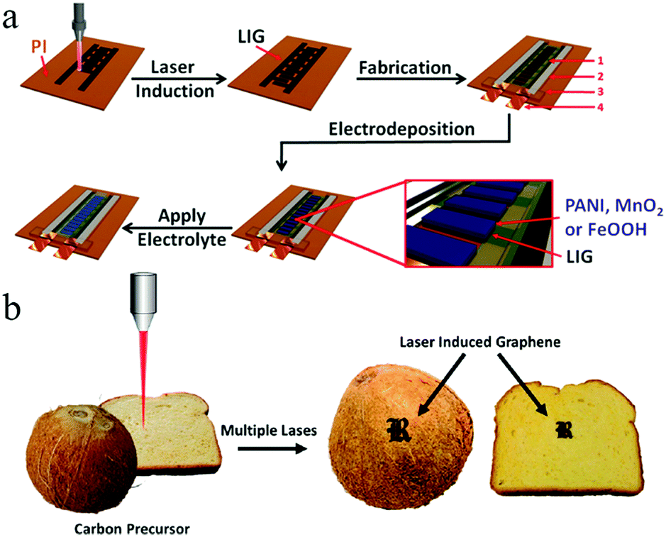
One problem that is difficult to solve in the microelectrode structure of an MSC is preventing electrical shorts between the positive electrode and the negative electrode.35 To date, researchers have experimented with many processing and manufacturing methods to build high-precision graphene-based MSC microelectrodes. Among these, lasers have been widely used in the machining of carbon-based MSCs, which can be employed as both a reduction method in reducing carbon oxides (such as GO48 and graphite oxide33) and a tool in directly performing micro/nanoprocessing.37 The use of convenient and inexpensive laser technology enables the on-chip integration of graphene-based MSCs and simultaneously enables continuous processing of graphene-based MSCs.Qu's group has demonstrated that fibrous graphene-based MSCs can be processed by laser reduction of GO.49,50 The sandwich structure of the all-in-one fibrous graphene-based MSCs consists of RGO as the electrodes and GO as the separator (Fig. 2a and b).49 Due to its overall structure, it possesses high mechanical and electrochemical properties. In the same way, a series of in-fiber graphene-based MSCs can be processed by region-specific reduction of a GO fiber (Fig. 2c and d).50 Hundreds of device units can be manufactured in a few minutes, suggesting the high efficiency of laser processing. Moreover, the MSCs have an area capacitance of 14.3 mF cm−2 and can be easily woven into a mesh. By employing a commercial Laser Scribe DVD burner, Kaner et al. produced graphene-based MSCs on a large scale without using a shielded mask.38 The obtained graphene-based MSCs exhibited superior mechanical and electrochemical properties. After 10000 charge/discharge cycles and 2000 bend/twist states, the graphene-based MSCs only lost 4% and 3% of their initial capacitance, respectively. Moreover, the MSCs achieved a volumetric capacitance of 3.05 F cm−3 at a current density of 16.8 mA cm−3. Graphene can be obtained not only by laser processing of carbon oxides, but also by laser induction of commercial polymers.51–57 Tour et al. used CO2 infrared lasers to synthesize on-chip integrated graphene-based MSCs on commercial polyimide (PI) sheets. The area capacitance of the laser-induced graphene (LIG) MSCs with aqueous electrolyte can reach up to 44 mF cm−2 at a scan rate of 20 mV s−1, which was close to that of GO-derived MSCs. These laser-induced large surface area graphene films from commercial PI exhibit excellent electrical conductivity. The in-plane LIG-MSC retained nearly 100% of its initial capacitance after 9000 cycles in aqueous electrolyte. In order to realize the storage of mobile energy, a simple and inexpensive self-charging micro-supercapacitor power unit (SCMPU) was programmed by integrating the MSCs with triboelectric nanogenerators (TENG).52 With a loading resistance of 20 MΩ, LIG-TENG provided a specific area power of 0.8 W m−2. The SCMPU could continuously light two LEDs and power a commercially available hygrothermograph. Because the laser does not destroy the internal structure of the heteroatom-doped graphene, it can be also used to prepare high-performance heteroatom-doped LIG-MSC. For example, boron-doped LIG-MSC delivered a higher capacitance of 16.5 mF cm−2 than non-doped MSC; N-doped LIG with PEDOT:PSS realized high conductivity and high electrochemical performance. The N-doped LIG-MSC with potassium polyacrylate–potassium hydroxide (PAAK/KOH) showed a high area capacitance of 0.79 mF cm−2 at a current density of 50 mA cm−2, which was also stretched to four times its original length. This assembled-MSC with flexibility and tensile properties can realize potential applications in micro and portable electronic devices in the near feature. Simultaneously, Tour and coworkers proposed an effective method to improve the performance of MSCs by introducing pseudo-capacitive materials (Fig. 3a).54 Among these, a laser was used to process PI films to produce patterned LIGs. Then, mixed electrodes, including LIG–MnO2, LIG-FeOOH, and LIG-PANI, were fabricated by the electrodeposition of MnO2, FeOOH or PANI on LIG, respectively. Finally, the MSCs without current collectors, binders, or separators were completed by dropping the electrolyte on them. On the one hand, the high-precision laser cutting of the PI substrate enables electrodepositing of pseudo-capacitive materials on the surface of LIG. On the other hand, LIG achieves high electrical conductivity and a large specific surface area. As a result, the resulting asymmetric in-plane LIG-FeOOH/LIG–MnO2 MSC could operate at a voltage of 1.8 V and obtain a specific area capacitance of 21.9 mF cm−2 with PVA/LiCl gel electrolyte at a current density of 0.25 mA cm−2, corresponding to a stack capacitance of 5.4 F cm−3. 84% of its initial capacitance was retained after 20000 charge/discharge cycles. The FeOOH/LIG–MnO2 MSC had a higher area power (11853 μW cm−2) than Li-thin film batteries. The use of laser technology to pattern graphene active material directly to form a microelectrode is a very effective and inexpensive method for on-chip integration of graphene-based MSCs.58–60 Wang et al. demonstrated that the use of picosecond lasers could facilitate the fabrication of graphene-based MSCs by preparing porous RGO films on glass substrates.58 The MSC possessed a high areal specific capacitance of 37.95 mF cm−2 at 0.6 mA cm−2 and 36.38 mF cm−2 at 10 mV s−1, surpassing many values of carbon active materials in all-solid-state MSCs. Kaner et al. developed a method for the direct engraving of porous graphene to produce patterned graphene-based MSCs.59 In this process, graphene can be prevented from accumulating by adding CNTs, and more channels are created to obtain more ions.61 Laser-scribed graphene (LSG)/CNTs-MSC demonstrates higher electrochemical performance than LSG-MSC. LSG/CNTs-MSC acquired an outstanding stacked capacitance of 3 × 10 F cm−3 at a current density of 1000 mA cm−3, a volumetric energy density of 0.84 mW h cm−3, and a volumetric power density of 1.0 W cm−3. In terms of cycle stability, it lost only 11.4% of its initial capacitance after 5000 charge/discharge cycles.
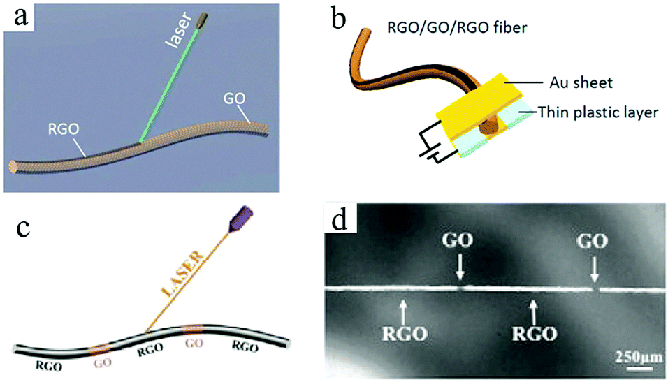 | ||
| Fig. 2 (a) Schematic of the laser reduction of GO fiber. (b) Scheme of the RGO–GO–RGO MSC device.49 (Reprinted with permission from The Royal Society of Chemistry. Copyright 2014.) (c) Scheme of the laser process of GO fiber. (d) Photograph of the bamboo-like structure of the GO fiber.50 (Reprinted with permission from The Royal Society of Chemistry. Copyright 2015.) | ||
 | ||
| Fig. 3 (a) Scheme of the fabrication of a graphene-based MSC.54 (Reprinted with permission from Wiley-VCH Verlag Gmbh. Copyright 2015.) (b) Schematic of the fabrication of laser-induced graphene on various substrates.64 (Reprinted with permission from American Chemical Society. Copyright 2018.) | ||
In addition, laser printing can be used to synthesize paper-based foldable planar graphene-based MSCs. Using this method, not only can silver nanowires (AgNWs) be inserted into the RGO layer to prevent stacking of layers, but the conductivity of electrodes without current collectors can also be improved.62 Wang and coworkers proposed coating graphene on flexible fabric to create flexible and lightweight in-plane MSCs which enable integrated applications of energy storage devices and wearable devices.63 The changes in electrochemical performance of the MSCs under bending or twisting conditions are almost negligible, which demonstrates their significant stability. Currently, Tour and coworkers are exploring the use of multiple lasers on various substrate materials (cloth, paper, food) to fabricate graphene-based MSCs (Fig. 3b).64 Basically, in addition to amorphous carbon, carbon precursors can be also converted to graphene on different substrates by employing multiple-laser technology. Conceptually, a LIG-MSC was constructed on the surface of a coconut; it demonstrated a high specific capacitance at 10 mV s−1, exceeding that of a lased polyimide MSC. This discovery provides a common method for synthesizing graphene-based MSCs on many types of substrates. Considering that MnO2 can improve electrochemical performance, Kaner's group employed 3D LSG–MnO2 electrodes to assemble symmetric and asymmetric MSCs.65 The symmetric LSG–MnO2 MSC delivered a higher areal capacitance (∼400 mF cm−2) than that in published studies on graphene-based MSCs. The integration of RGO and Au nanoparticles (NPs) was demonstrated by Hu et al. (Fig. 4); this is a facile approach to fabricate high-rate graphene-based MSCs.66 A GO/HAuCl4 mixture is spread onto a photo paper to obtain a GO/HAuCl4 hybrid film. The film is processed by direct femtosecond (FS) laser writing to form patterned RGO/Au electrodes. Electrolyte is then dropped onto the RGO/Au MSC. In fact, a proof-of-concept 3D RGO/Au FS MSC was obtained by a layer-by-layer drop-casting/laser-writing method. The 3D RGO/Au FS MSC delivered more capacitance retention at a high scan rate than a 2D single-layer MSC. For example, the 3D RGO/Au MSC retained 49% and 23% of its initial capacitance when the charge rates ranged from 0.1 V s−1 to 10 V s−1 and from 0.1 V s−1 to 100 V s−1, respectively. Notably, the specific capacitances were 4.92 mF cm−2, 2.39 mF cm−2, and 1.12 mF cm−2 when the scan rates were 0.1 V s−1, 10 V s−1 and 100 V s−1, respectively. Similarly, Shanov and coworkers have developed a simple and feasible method for constructing 3D graphene-based MSCs using laser processing graphene.67 In this design, graphene is both a porous current collector and an active electrode material that can be used to provide multifunctional energy storage. Studies have shown that 3D graphene-based MSCs achieved an area capacitance of 1.5 mF cm−2 at a high scan rate of 10 V s−1, as well as a high power density (14.4 mW cm−2) and energy density (0.38 μW h cm−2). In addition, under different bending angles, the 3D-GP MSCs retained 100% of their initial capacitance and maintained an outstanding cyclic life after 20000 charge/discharge cycles.
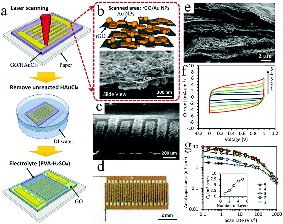 | ||
| Fig. 4 (a) The fabrication of GO/Au-MSC. SEM images of the RGO/Au microelectrodes with high magnification (b) and low magnification (c). (d) Photograph of the as-prepared MSC. (e) SEM image of the 5-layer 3D RGO/Au microelectrode. (f) CV curves for different numbers of layers. (g) Areal capacitance at different scan rates. Inset: Areal capacitance for different numbers of layers.66 (Reprinted with permission from The Royal Society of Chemistry. Copyright 2016.) | ||
2.4 Printing technology
Because it is inexpensive and involves minimal waste of materials, printing can be used as a promising technology and has very broad application prospects in the manufacture of electronic devices.The general principle of printing is to prepare the active material as a solution and print it on a substrate according to a predetermined pattern. Printed electronic devices can be easily adapted to factory production equipment and are readily constructed on flexible substrates, which facilitates amplifying the processing of flexible electronic devices.68 Printing technology also plays an important role in the manufacture of graphene-based MSCs. Chen's group realized the fabrication of graphene-based interdigitated electrodes by gravure printing of crumpled graphene hybrid ink.69 In this work, Mg(OH)2 not only prevented the re-stacking of graphene layers, but also provided the graphene with more oxygen-containing functional groups. Finally, the as-produced 2D graphene-based MSCs with PVA/H2SO4 gel electrolyte presented excellent stacked energy densities up to 1.41 mW h cm−3 and 0.35 mW h cm−3 at power densities of 25 mW cm−3 and 300 mW cm−3, respectively. Screen printing is also a simple and low-cost method to build thin film MSCs based on flexible polyethylene terephthalate (PET).70 The silver paste is screen-printed on the PET surface to act as a current collector. The N-doped RGO is then coated on the silver surface and the PVA/H3PO4 gel electrolyte is dropped on the coated surface. The all-solid-state planar MSC showed a high area capacitance of 3.4 mF cm−2. In addition to screen printing technology, ink printing technology is an effective and facile method for the scaled-up production of graphene-based MSC devices.71–74 Previous studies have shown that the GO solution can serve as a printing ink after being concentrated.71 GO is then chemically reduced to synthesize interdigitated electrodes. PVA/H2SO4 is dropped on the surface of RGO to complete the fabrication of the all-solid-state MSCs. It is convenient to increase the thickness of the RGO electrodes by repetitive layer-by-layer printing to obtain a higher specific area capacitance for MSCs. At the same time, Song et al. used 3D printing technology to explore a new method of manufacturing MSCs with extremely high mechanical flexibility.75 The distilled GO ink is affixed to interdigital current collectors and the 3D MSC electrode materials are formed by freeze-drying, reduction and vacuum drying. Considering the performance and effectiveness of the MSCs, 4-layer active materials are considered to be the best choice for MSCs. The assembled 3D MSCs exhibited an area capacitance of 56.7 mF cm−2 at 5 mV s−1 and a specific mass capacitance of 7.37 F g−1 at 0.1 A g−1 compared to those of 3D-printed graphene SCs. Although the 8-layer MSC achieved a higher area capacitance of 74.31 mF cm−2 at 5 mV s−1 than the 4-layers MSC, it only retained 56.5% of its initial capacitance when the scan rate was increased to 200 mV s−1.
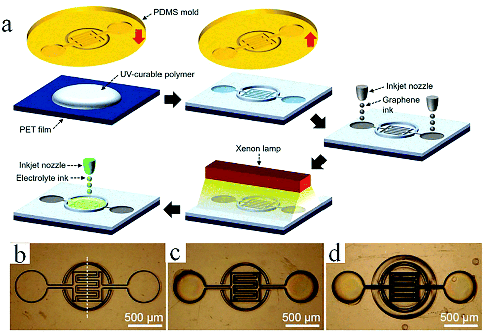
In general, direct printing of graphene or its composites is more convenient and common than printing GO after reduction. For example, Östling's group constructed graphene-based MSCs by printing graphene ink directly on a transparent glass substrate.74 Subsequently, excess graphene could be etched away by O2 plasma with the help of a printing mask. The mask was removed, and the all-solid-state MSC was obtained by dropping the electrolyte. Hersam et al. demonstrated the printing of graphene and ethylcellulose (G/EC) hybrid electrodes on a flexible substrate by inkjet printing.72 The all-solid-state flexible MSC with PVA/H3PO4 gel electrolyte presented distinguished cycle stability (minimal capacitance loss after 10000 charge/discharge cycles) and mechanical performance (no obvious capacitance loss after >5000 bending cycles). Simultaneously, Frisbie's group also mentioned in their work that by combining inkjet printing with self-aligned capillary assisted lithography (SCALE), they obtained a flexible all-solid-state MSC (Fig. 5).68 In this work, UV-assisted curved polymers were used as the capillary channels and receivers. Graphene ink readily filled the receivers and microfluidic channels under capillary action. Therefore, this process enables the accurate mass-production of flexible MSCs. The as-obtained graphene-based MSCs provided a superb area capacitance and could produce 44 devices in a tiny site area (<1 mm2 per MSC area) with 100% yield while maintaining an accurate lateral spatial resolution of 20 μm, which reflects the high accuracy and high success rate of this inkjet printing and SCALE processing method. Recently, a full inkjet printing method was explored to develop the large-scale and facile manufacture of thin-film MSCs based on graphene.76 Specifically, graphene acts as a current collector and the electrode in the MSC at the same time. The thin-film MSC with polymer gel electrolyte achieved a specific capacitance of 0.7 mF cm−2 at 10 mV s−1. Meanwhile, the full inkjet printing method simplifies the entire production process; as a consequence, it enables one-step, inexpensive manufacture of printed graphene-based MSCs with multiple connection methods. In addition, an on-chip integrated MSC array consisting of more than 100 devices achieved a 12 V voltage output without packing, even after eight months. In addition to the printing methods mentioned above, spray-coating is a promising method for the manufacture of graphene-based planar MSCs.77–79 Asymmetric MSCs can be easily fabricated by spraying 2D titanium carbide (Mxene) as a negative electrode and RGO as a positive electrode on a flexible transparent PET sheet.77 Poly(3,4-ethylenedioxythiophene):poly(styrenesulfonate) (PH1000) can effectively prevent stacking of the exfoliated graphene (EG) sheets and act as a surfactant to increase the wettability of EG. The micro-interdigitated electrodes can be obtained on various substrates by spray-coating the EG/PH1000 composite materials with a mask. The as-prepared paper-based MSCs displayed a specific capacitance of 5.4 mF cm−2 at a scan rate of 1 mV s−1.78 Notably, a novel and facile spray-coating technique has been also precisely designed for the synthesis of linear tandem graphene-based MSCs (LTMS) on various substrates (Fig. 6).79 The LTMS is one-step manufactured on paper by a similar method of spray-coating EG/PH1000 composite inks with pre-customized masks. However, unlike other masks, this mask is a discontinuous parallel linear custom mask. The graphene-based LTMS (10MSCs) were charged to 8 V with PVA/H2SO4 gel electrolyte, while the single MSC was charged to 0.8 V.
 | ||
| Fig. 5 (a) Schematic of the fabrication of MSC by the SCALE method. (b–d) Optical photographs of MSC during synthesis at different stages.70 (Reprinted with permission from Wiley-VCH Verlag Gmbh. Copyright 2017.) | ||
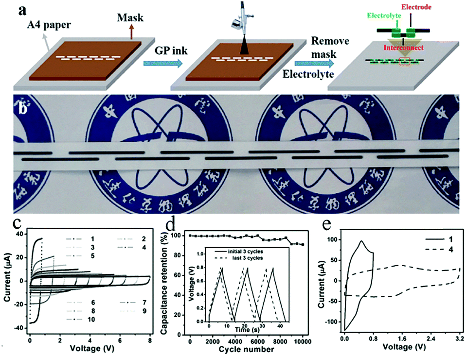 | ||
| Fig. 6 (a) Scheme of the fabrication of series-connected graphene-based MSCs. (b) Photograph of the series-connected MSCs on paper. (c) Cyclic voltammogram of graphene-based MSCs with increasing numbers of serial MSCs at a scan rate of 100 mV s−1. (d) Cycling stability of the MSCs after 10000 charge and discharge cycles. Inset: Galvanostatic charge–discharge curves of the MSCs at the initial and last three cycles. (e) Cyclic voltammogram of 4 series MSCs at 50 mV s−1 compared with a single MSC.79 (Reprinted with permission from Wiley-VCH Verlag Gmbh. Copyright 2017.) | ||
In addition, the final capacitance could reach 94% of the original capacitance in a bent state, which indicates excellent mechanical flexibility. The addition of a pseudo-capacitive material significantly improved its capacitive performance (7.6 mF cm−2 at 2 mV s−1). In addition to the symmetric LTMS, the asymmetric LTMS are fabricated by an analogous approach (MnO2 as the positive electrode, EG as the negative electrode). The asymmetric LTMS arrays possessed a high voltage of 5.4 V, which is twice as high as that of a single device. In a word, this work develops a simple and facile spraying method for manufacturing flexible high-voltage MSCs, paving the way for the provision of MSCs for electronic devices in daily life.
2.5 Oxygen plasma treatment
O2 plasma treatment is an extremely efficient and simple method to etch graphene and graphene-based composites to build patterned micro-finger electrodes.39,80–90 The general procedure for fabricating graphene-based MSCs using O2 plasma treatment is as follows: first, a metal is sprayed with a mask on the film surface to form the desired pattern for the current collector. Then, the uncovered active material is etched away by O2 plasma to obtain the MSCs. For example, Müllen et al. reported that GO was spin-coated on a silicon wafer and then reduced by CH4 at 700 °C.39 O2 plasma was used to etch the graphene. The planar MSCs revealed a high area capacitance of 80.7 mF cm−2 and a power density of 495 W cm−3. Graphene-based composites and heteroatom-doped graphene can be also treated with O2 plasma to form MSCs with enhanced capacitance and energy storage. A nitrogen precursor of poly-L-lysine (PLL) and a boron precursor of H3BO3 are incorporated into the multilayer films to obtain the boron–nitrogen co-doped graphene (BNG) hybrid films (Fig. 7).88 After the patterned Au is deposited on the surface of the film, the BNG-MSCs are patterned by O2 plasma etching. At the same time, sulfur-doped graphene (SG) film is obtained from the peripheral trisulfur-annulated hexa-peri-hexabenzocoronene (SHBC). The SHBC film is sequentially subjected to high temperature, Au plating and O2 plasma to obtain the patterned MSCs. The resulting SG-MSCs with H2SO4/PVA displayed an unprecedented volumetric capacitance density of 8.1 F cm−3 at 2000 V s−1 and a volumetric power density of 1191 W cm−3. Moreover, the SG-MSCs possessed a short time constant (0.26 ms) and a stacked capacitance of 582 F cm−3 at 10 mV s−1.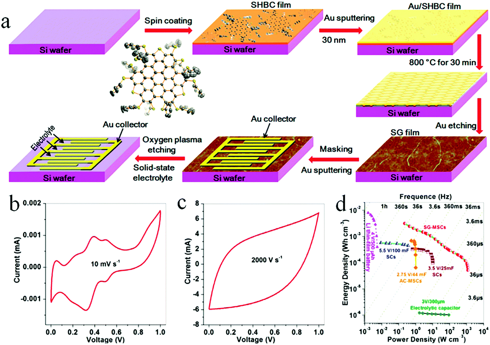 | ||
| Fig. 7 (a) Scheme of the fabrication of an in-plane MSC on a Si/SiO2 wafer by O2 plasma treatment. Cyclic voltammetry of the MSC tested at (b) 0.01 and (c) 2000 V s−1. (d) Ragone plot of the MSC in comparison with commercially available energy storage devices.88 (Reprinted with permission from American Chemical Society. Copyright 2017.) | ||
In addition, EG and pseudo capacitive materials such as PANI can be assembled into MSCs which integrate the properties of an electric double layer capacitor with the properties of Faraday pseudocapacitors.82 The resulting MSCs with PVA/H2SO4 presented a specific capacitance of 368 mF cm−2 and a stacked capacitance of 736 F cm−3 at a scan rate of 10 mV s−1. Furthermore, the in-plane MSCs delivered a stacked energy density of 46 mW h cm−3 and negligible capacitance performance loss in a bent state. Similarly, TP/EG-MSCs provided very high rates and stacking capacitance by alternately stacking EG nanosheets (<3 layers) and thiophene (TP) nanoplatelets.89 An O2 plasma treatment method has also been used to combine EG and PANI to obtain a composite film and then process it into MSCs. Unlike the layer-by-layer alternative assembly method of EG and PANI, aniline polymerizes on the surface of graphene to form mesoporous PANI. The thus-assembled MSCs typically operate at very high scan rates, surpassing traditional MSCs. More importantly, the MSCs represented a significant volumetric power density of 600 W cm−3 and a volumetric energy density of 6.67 mW h cm−3, which are very close to those of lithium thin-film batteries. Another study shows that in addition to TP/EG and graphene–PANI hybrid film interdigital electrodes, a ternary composite film composed of RGO/MnO2/AgNW can be processed by O2 plasma to form interdigital electrodes.84 The MSCs realized a very short time constant of τ0 = 0.14 ms and operated normally at 50000 mV s−1 with ionic liquid gel electrolyte. Inspired by leaf veins, Lee et al. used a dense assembly of RGO with 2D nanochannels constructed from Cu(OH)2 nanowires (NWs) to design ion transport in MSCs (Fig. 8).86 Poly diallyldimethylammonium chloride (PDDA) not only hinders the stacking and aggregation of GO but also improves the energy storage of graphene-based MSCs by the introduction of heteroatoms. In the preparation process, a PDDA, GO and Cu(OH)2 NWs mixture solution is filtrated to form a hybrid film. By chemical reduction of GO, the obtained film undergoes O2 plasma treatment before patterned Au is deposited on the film. The resulting MSC with PVA/H2SO4 electrolyte produced a distinguished stacking capacitance of 348 F cm−3, which is equivalent to an area capacitance of 409 mF cm−2. This result clearly exceeds that of carbon-based solid-state MSCs. This MSC achieved a stack energy density of 6.7 mW h cm−3 at a stack power density of 0.1 W cm−3 and a short time constant (33 ms) as well as long term cycle stability (8% of initial capacitance deterioration after 5000 charge/discharge cycles).
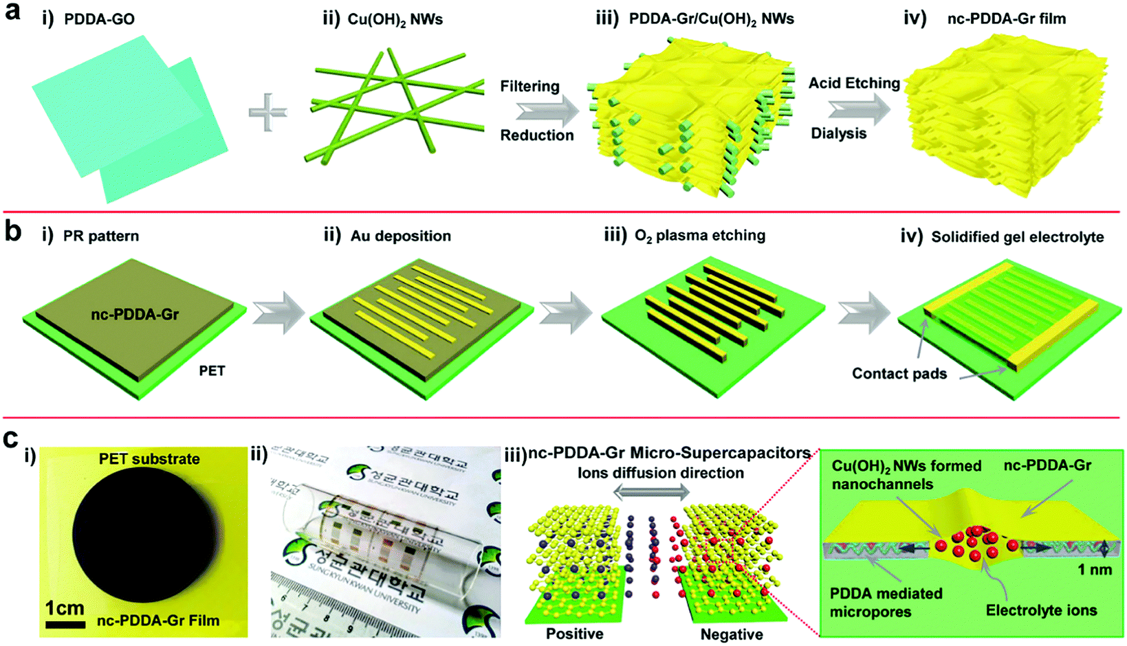 | ||
| Fig. 8 Scheme of the fabrication of the nc-PDDA-Gr MSC. (a) Schematic of the synthesis process of the nc-PDDA-Gr film. (b) Fabrication of the MSC. (c) Photograph of the as-produced MSC and a scheme of the ion transport pathway.86 (Reprinted with permission from Wiley-VCH Verlag Gmbh. Copyright 2015.) | ||
In order to visualize the storage energy of MSCs, Feng et al. integrated the EG with an electrochromic material (V2O5) as a hybrid electrode material.85 The exposed EG/V2O5 hybrid films were etched by O2 plasma to obtain patterned MSCs. The obtained stimulus-responsive MSCs exhibited significant reversible electrochromism upon charge/discharge in a potential window of 0 to 1 V, which provides direct visual observation of the different energy storage stations of the MSC. If graphene-based MSCs are expected to be used for photo switchable sensors, they must possess extremely high rate capacitance. Müllen et al. demonstrated that an MSC assembled from diarylethene (DAE) and graphene hybrid electrodes had the above advantage and could be applied to photo-switchable sensors.90 DAE is interconverted between two thermodynamically stable photoisomers by UV or white light irradiation. The in-plane MSC combines the efficient photochromic properties of DAE and the reversible control of electric double layer capacitors. As a consequence, the MSC operated normally at an extremely high rate of 104 V s−1, four orders of magnitude higher than that of conventional MSCs. The specific capacitance of the MSC improved linearly when the MSC was exposed to UV light, while the specific capacitance returned to the initial state when the MSC was exposed to white light irradiation.
2.6 Photolithography
The conventional nanoscale photolithography method is another effective approach for preparing graphene-based MSCs. Generally, a photoresist is first coated on the surface of the active material film and exposed under the action of a mask to obtain a patterned photoresist. Metal deposition is then performed to remove the remaining photoresist. After etching away the active material that is not covered by the metal, the patterned MSC is finally obtained. For example, Feng et al. used photolithography to pattern RGO films on Si wafers to form MSCs.91 In addition to the pure RGO film, RGO and CNTs composite films can be also processed into MSCs by photolithography.92,93 Wong and coworkers developed a self-assembly method on a metal microelectrode and reduced GO to prepare all-solid-state MSCs by the same method.94 To improve their electrochemical performance, porous G/PANI composites were used as the active materials to promote ion accessibility and adsorption.95 The GO solution is dropped on the current collectors and is chemically reduced. PANI is then deposited on the surface of graphene. The photolithography-assisted MSCs delivered superior volumetric capacitance and energy density. Furthermore, by alternatively spin-coating the MoS2@RGO/photoresist and CNT/photoresist composites twice, after pyrolysis, the as-prepared MSCs could supply an area capacitance of 13.7 mF cm−2 and an energy density of 1.9 μW h cm−2 at a current density of 0.1 mA cm−2.96 Moreover, the MSCs demonstrated rate capacitance (32% of capacitance lost at 2 mA cm−2) and cycle stability (only 3.4% of capacitance lost at 1 V s−1 after 10000 cycles). In general, an interdigital electrode cannot withstand high tension due to its rigid characteristics and planar structure.97 To solve this problem, Chen's group produced high-stretch graphene-based MSCs using photolithographic techniques (Fig. 9).97 In short, the patterned photoresist is deposited on a Cu film. The GO solution fills the photoresist-uncovered area and forms GO ribbons. After the ribbons are transferred to a tripod PDMS substrate, Cu and the photoresist are removed using chemical reagents to obtain the MSCs. The MSCs showed no significant degradation in performance at 100% strain and lost only 8% of their original capacitance after 5000 stretching/relaxing cycles, indicating that the assembled MSCs had good extensibility. This is mainly due to the removal of stains by the suspended wavy graphene ribbon arrays to avoid cracks; also, the unchanged distance between the electrode fingers maintains the stability of the MSCs during the stretching/relaxing cycles. At present, in most 2D thin-film MSCs, because the volumes of some active materials are small, more charges cannot be stored; as a result, they cannot play greater roles in microelectronic devices.47 In order to address the shortcoming of the low energy density of thin-film MSCs, researchers must load more active materials per unit electrode area. For example, Tour et al. designed 3D graphene/CNT carpet-based MSCs (G/CNTC-MSCs) on nickel electrodes by photolithography.98 The G/CNTCs-MSCs delivered an impedance phase angle of −81.5 at a frequency of 120 Hz and a volumetric energy density of 2.42 mW h cm−3 in ionic liquid. Additionally, the G/CNTCs-MSCs operated at 400 V s−1 to achieve a superb power density of 115 W cm−3 in 1 M Na2SO4 solution.
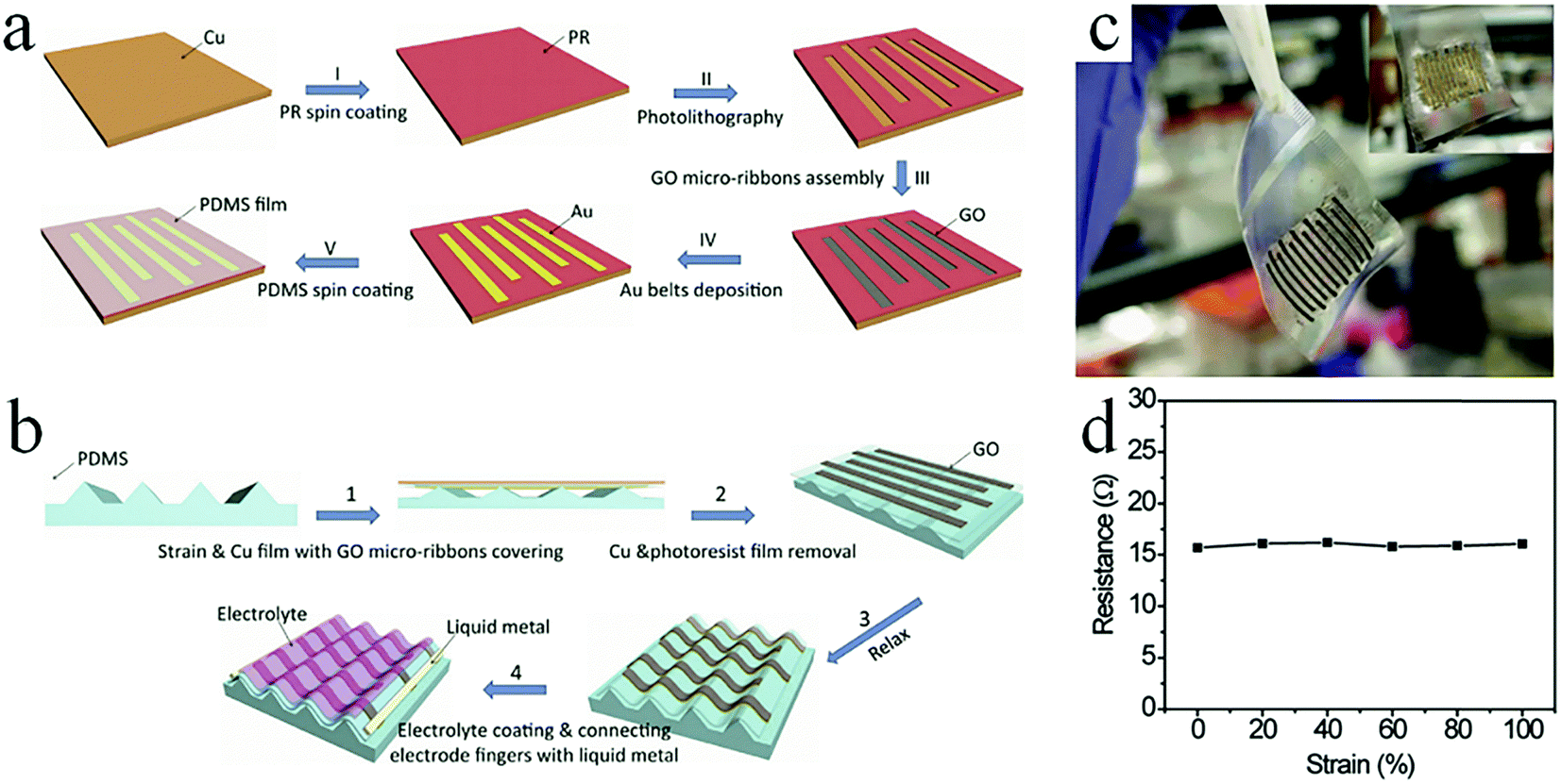 | ||
| Fig. 9 (a) Schematic showing the fabrication of GO electrode arrays using photolithography. (b) The transfer process of electrode arrays to the tripod-structured PDMS. (c) Photograph of the stretchable graphene-based MSC. Inset: The gold belt side. (d) Resistance of the electrode arrays with increased strain.101 (Reprinted with permission from Wiley-VCH Verlag Gmbh. Copyright 2015.) | ||
2.7 Electrochemical deposition
Graphene-based symmetric and asymmetric MSCs can also be obtained by electrochemical deposition. In general, the synthesis steps are as follows: a metal current collector is built on the substrate. The active material is then electrochemically deposited on the metal current collector. Finally, electrolyte is dropped onto the film to complete the MSCs. As reported by Yan et al., a symmetric MSC was manufactured by electrochemical deposition of graphene quantum dots on both electrodes, while an asymmetric graphene-based MSC was fabricated by electrochemical deposition of graphene quantum dots (as the negative electrode) and polyaniline (as the positive electrode).99,100 Metal oxides are often incorporated into graphene-based MSCs as highly pseudocapacitive materials. Metal oxides and graphene as the two electrodes in asymmetric MSCs can effectively improve their capacitance and potential windows. For example, Co(OH)2 and RGO as active materials are electrodeposited on the surface of the current collectors, respectively.101 Recently, Niu's group proposed a novel approach to spontaneously reduce GO/GO composites and assemble RGO sheets on interdigital electrodes (Fig. 10).102 The interdigitated Au current collectors are deposited on PET film with a shield. Zn is electrodeposited on one side of the electrode to reduce and assemble GO/Mn3O4. Then, Zn is electrodeposited on the other side of the electrode to reduce the GO and assemble the RGO sheets. The as-prepared asymmetric MSC exhibits excellent electrochemical performance as well as significant mechanical properties.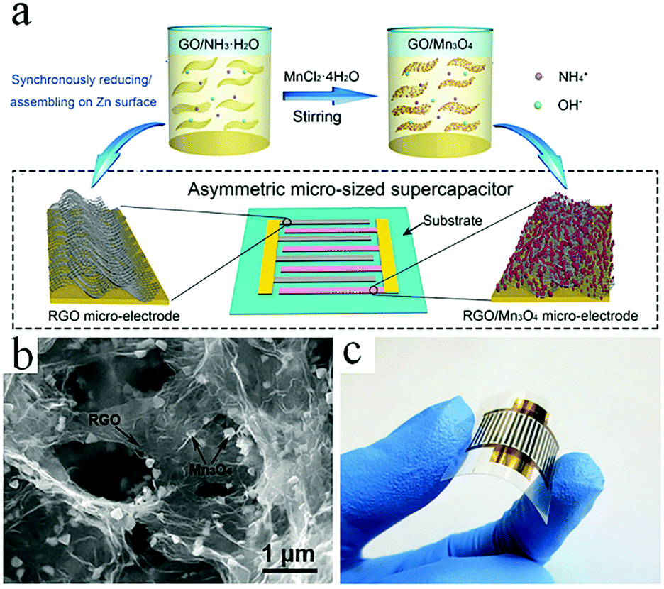 | ||
| Fig. 10 (a) Scheme of the reducing/assembling procedure used in the fabrication of RGO and RGO/Mn3O4 electrodes. (b) SEM image showing the morphologies of RGO and Mn3O4. (c) Photograph of the RGO//RGO/Mn3O4 MSC.102 (Reprinted with permission from Wiley-VCH Verlag Gmbh. Copyright 2018.) | ||
2.8 Other processing methods
Although graphene-based MSCs can be regarded as very promising energy storage devices, precise and efficient construction of micro/nano electrodes is still a key step that represents a difficulty in the completion of MSCs. To address this issue, researchers are exploring other novel and practical methods of manufacturing MSCs.Qu et al. achieved large-scale production of on-chip integrated graphene-based MSCs through a press-assisted template method (Fig. 11).103 The graphene-based MSCs were fabricated on various substrates and adhered tightly to the substrates. The resulting MSCs showed an excellent specific capacitance of 41.6 mF cm−2 at a current density of 8.4 mA cm−2 and retained 82.5% of their initial capacitance after 1000 charge/discharge cycles. Majumder's group chose focused ion beams (FIB) direct-write technology to build patterned graphene-based MSCs.104 Similar to laser engraving, FIB can selectively reduce graphene oxide and pattern the GO film. During the preparation process, the size of the MSCs can be also regulated by adjusting the ion beam. Due to the high conductivity of graphene, the presence of graphene can significantly improve the electrochemical performance and charge storage ability of graphene-based planar MSCs. Moreover, ultraviolet light is an efficient way to reduce GO and TiO2 composites (Fig. 12).105 Under irradiation of ultraviolet light, the exposed GO/TiO2 is reduced with a mask to obtain patterned RGO/TiO2 hybrid electrodes. It is shown that this photocatalytic reduction of GO/TiO2 composite films to form highly conductive micro-RGO/TiO2 electrodes can realize large-scale production of graphene-based MSCs on different substrates, which is also very effective and can be completed in one step. Kim et al. reported that pen lithography is a simple method to fabricate MSCs based on graphene/PEDOT electrodes.106 Before the graphene/PEDOT composites are drawn on PET, a 10 interdigitated finger line pattern is printed on the PET substrate. The layer-by-layer graphene/PEDOT microelectrodes constructed in this way showed good electrical conductivity and structural integrity. Furthermore, phosphorene is a promising 2D material, similar to graphene, due to its high conductivity and fast ion diffusion properties. Phosphorene/graphene (PG) hybrid electrodes obtained by vacuum filtration with a mask are transferred onto the PET film, and then the electrolyte is dripped on them to complete the MSCs (Fig. 13).107 It is possible to obtain layer-by-layer PG hybrid microelectrodes in one step. This approach simplifies the production of series or parallel MSCs with custom masks and effectively avoids the use of metal connectors. Therefore, this cost-effective and facile strategy can potentially create on-chip integrated MSCs. MSCs with sandwich structures are fabricated using vertically oriented sheets of active materials and inserting a solid electrolyte or a separator with electrolyte between two electrodes to prevent short circuits.108–110 The active materials are always grown in arrays perpendicular to the substrate to promote ion diffusion and increase the surface area. Pech's group designed a microelectrode constructed from porous RuO2-modified vertically oriented graphene sheets.108 At the same time, they used PVA/H3PO4 gel electrolyte to solve the leakage problem while assembling all-solid-state MSCs. Similarly, in another study, Bao et al. used a thermal decomposition method to grow vertically aligned graphene unidirectional arrays on SiC to form electrodes (Fig. 14).110 The strong interaction between graphene and the current collector effectively decreases the resistance and increases the diffusion of ions. Thus, graphene-based MSCs can normally operate at 200 V s−1, whether in PVA/H2SO4 or 1-ethyl-methylimidazolium tetrafluoroborate electrolyte. Moreover, the MSCs exhibited a fast frequency response (9 ms) and high capacitance (∼7.3 mF cm−2).
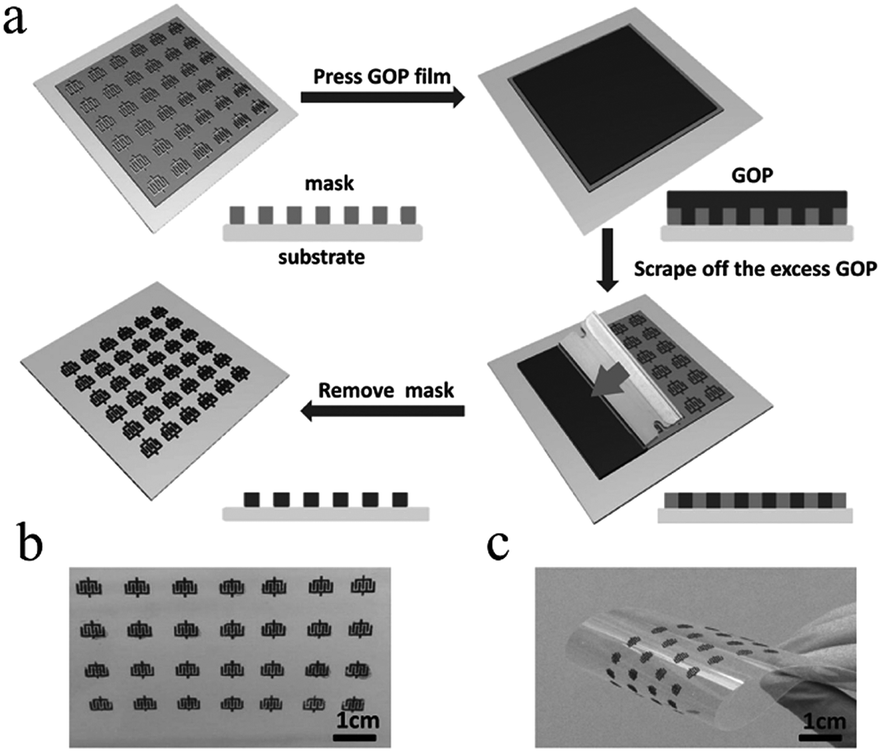 | ||
| Fig. 11 (a) Scheme of the press-assisted template process of on-chip integrated graphene-based MSCs on various substrates. Photographs of on-chip integrated graphene-based MSCs in (b) flat and (c) bent states. 103 (Reprinted with permission from Wiley-VCH Verlag Gmbh. Copyright 2016.) | ||
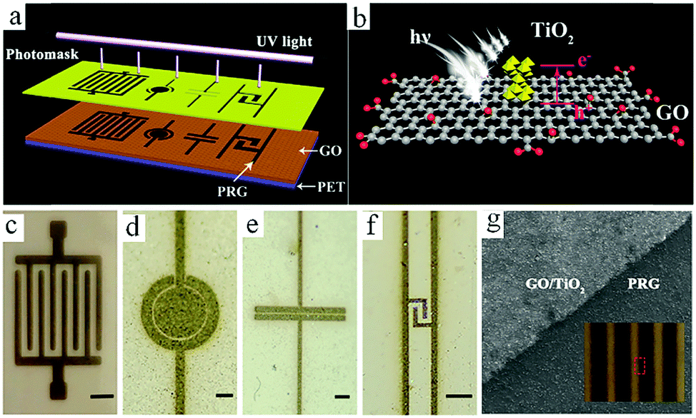 | ||
| Fig. 12 (a) Scheme of the process to obtain photochemically reduced MSCs with various shapes. (b) The mechanism of TiO2-assisted reduction of a GO film. (c–f) PRG-MSCs with various patterns. Scale bars: 250 mm (c) and 500 μm (d–f). (g) SEM image of a PRG film displaying the boundary between GO/TiO2 and the PRG film. Inset: Optical image of the processed PRG film.105 (Reprinted with permission from American Chemical Society. Copyright 2017.) | ||
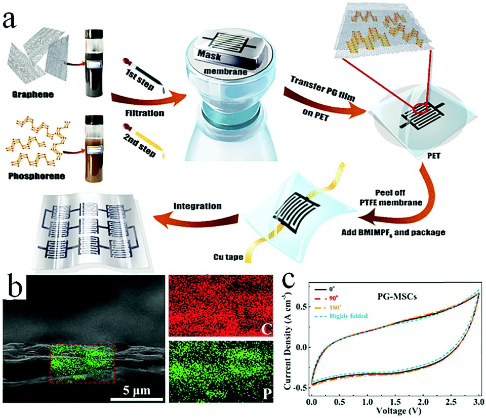 | ||
| Fig. 13 (a) Scheme showing the fabrication process of PG-MSCs. (b) Cross-section SEM image of a PG film (left) and the corresponding EDX mapping (right). (c) CV curves of the MSC in various bending positions at 100 mV s−1.107 (Reprinted with permission from American Chemical Society. Copyright 2017.) | ||
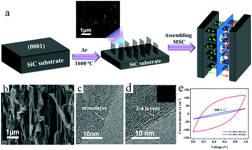 | ||
| Fig. 14 (a) The fabrication of VG-MSCs on a SiC substrate. (b) Cross-section SEM images of VG. (c) Monolayer and (d) multilayer VG. Inset in (d): A SAED image. (e) CV curves of different MSCs obtained at 200 V s−1.110 (Reprinted with permission from American Chemical Society. Copyright 2017.) | ||
3 Summary and prospects
Graphene has advantages of ultra-thin layer structure, good conductivity, light weight, etc.; thus, it is undoubtedly a very promising electrode material for energy storage devices. At the same time, along with the development of portable and tiny electronic devices, many efforts have been devoted to the processing of graphene-based MSCs, including 1D, 2D, 3D and traditional sandwich-type structures. Here, we have summarized the recent advances in graphene-based MSCs and discussed the different types of MSCs, including 1D, 2D 3D and traditional sandwich-type structures; we have also elaborated on their processing methods.Hydrothermal methods or wet spinning methods are always employed to produce 1D graphene-based MSCs in the form of graphene fibers, which have greatly increased specific surface areas and ion availability. Graphene doped with heteroatoms or decorated with pseudocapacitive materials can achieve greatly enhanced energy density and power density by the hydrothermal method or wet spinning method. The flexibility and the facile weaving nature of fibers enable 1D graphene-based MSCs to achieve potential applications in wearable electronic devices. Despite the advantages of 1D graphene-based MSCs, their stretchability is unsatisfactory. The MSCs are fragile if an external force is applied. Due to complex processes and harsh production environments, they are difficult to adapt to large-scale production, which is still a vital issue to be addressed. Numerous approaches can be used to process 2D graphene-based MSCs with interdigital shapes, such as laser engraving, printing, and photolithography. These processing technologies are closely related to the architectures of graphene-based MSCs. In a sense, it is necessary to understand the effects of different processing methods on the performance of graphene-based MSCs so that appropriate technologies can be selected to process them. The length and width of the interdigitated fingers and the interspaces between adjacent electrodes have enormous influences on the electrochemical performance of MSCs. Narrow interdigitated electrodes and small interspaces can shorten the path that the electrolyte ions must pass through to reduce the electrical resistance and increase the energy and power density of the device, if the lengths and numbers of the interdigitated electrodes are constant. This synergistic effect can be used to improve the electrochemical performance if the length, width, numbers and interspaces have an optimal relationship. Consequently, we need to further systematically explore the effects of interdigitated electrodes on electrochemical performance and improve our overall understanding of the architecture of MSCs. Even when the density of the active materials is increased, the energy of 2D MSCs still cannot meet the requirements of electronic equipment. Thus, the development of 3D MSCs is a very important and sensible choice to address this problem. To a large extent, the processing methods for 3D MSCs are the same as those for 2D MSCs. However, it should be noted that the processing technologies for 3D MSCs need more stringent requirements and accuracy. Compared to 2D MSCs, almost-3D MSCs present higher specific energies and power densities due to the thicker active materials on the same footprint. The diffusion rate of the electrolyte ions and the pathway that the ions need to pass through do not change as the active materials thicken. The boundary between the 3D MSCs and the macro SCs will become blurred if the active materials are thickened to a certain degree, which makes it difficult to choose appropriate parameters to evaluate its electrochemical performance. However, 3D MSCs are newly promising energy storage devices; many efforts are still being paid to explore large-scale and simple processing techniques. The classic sandwich structure of graphene-based MSCs is readily assembled, while the vertical growth of active material sheets is complicated to achieve. The vertical arrays of layer structures not only increase the specific surface area but also promote the diffusion of ions. Moreover, some crucial factors affect the development of graphene-based MSCs. First, the active materials play a significant role in the electrochemical reactions of MSCs. Thus, we need to ensure that the processing methods do not destroy the structure and composition of the active materials. Both graphene and graphene-based composites should have the essential properties of high specific surface area, high conductivity, and porosity to facilitate the diffusion of ions and electrons to reduce the device resistance, leading to high electrochemical performance. Indeed, heteroatom (S, N) doping of graphene can significantly increase its charge storage capacity. Moreover, without destroying the graphene sheet structure, pseudocapacitive materials, which always include a metal oxide (MnO2, RuO2etc.) and conductive polymer (PEDOT, PANI etc.), are also employed to decorate graphene to enhance its electrochemical performance. This will not only cause different charges to accumulate at different electrodes but will also cause a rapid and reversible reaction, combining the properties of electrochemical double-layer capacitors and pseudocapacitors. Second, the electrolyte is also a crucial part of graphene-based MSCs; these include aqueous electrolytes and ionic liquids. Aqueous electrolyte is relatively safe due to its non-flammable and non-explosive nature. Additionally, aqueous electrolyte has high ionic conductivity; thus, it has been widely used in traditional MSCs in the past. However, leakages and serious difficulties in packaging constrain its usage. Although the ionic conductivity of all-solid-state electrolytes is lower than that of liquid electrolytes, all-solid-state electrolytes are more often used in microelectronic devices. After curing for some time, the all-solid-state electrolyte can be tightly attached to the surface of the electrode to avoid leakage. Ionic liquid electrolytes can not only broaden the potential window of graphene-based MSCs but can also drastically increase their specific energy density; however, the flammability of ionic liquid electrolytes must be addressed. In short, more research should be devoted to developing all-solid-state electrolytes that balance safety and high performance. Last but not least, suitable processing methods should be used to optimize the construction structures of graphene-based MSCs, which is essential to improve their mechanical and electrochemical performance. That is, graphene-based MSCs are not only small but should take advantage of the synergy between the electrodes, substrate and electrolyte. It is noteworthy that the processed architectures of graphene-based MSCs must possess flexible and stretchable properties without compromising electrochemical performance. In addition, taking into account the problems of production and processing, the architectures of graphene-based MSCs should be simplified as much as possible to enable their adaptation to cost-effective and large-scale industrial production.
Although much progress has been made in the development of graphene-based MSCs, this research is still in its infancy; these MSCs are far from meeting the requirements of practical energy storage electronics. There is still enormous room for improvement in the active materials, electrolytes, and architectures of these MSCs. Based on these considerations, we are confident that more excellent graphene-based MSCs will be created through the joint efforts of researchers.
Conflicts of interest
There are no conflicts to declare.Acknowledgements
This work was supported by the National Key R&D Program of China (2017YFB1104300 and 2016YFA0200200), NSFC (No. 21671020, 51433005 and 51673026), NSFC-MAECI (51861135202), Beijing Natural Science Foundation (2172049 and 2152028), and Beijing Municipal Science and Technology Commission (Z161100002116022 and Z161100002116029).Notes and references
- Z. L. Wang, Adv. Mater., 2012, 24, 280–285 CrossRef PubMed.
- J. G. Koomey, H. S. Matthews and E. Williams, Annu. Rev. Environ. Resour., 2013, 38, 311–343 CrossRef.
- H. Sun, Y. Zhang, J. Zhang, X. Sun and H. Peng, Nat. Rev. Mater., 2017, 2, 17023 CrossRef.
- P. Simon and Y. Gogotsi, Nat. Mater., 2008, 7, 845 CrossRef PubMed.
- Z. Lei, J. Zhang, L. Zhang, N. Kumar and X. Zhao, Energy Environ. Sci., 2016, 9, 1891–1930 RSC.
- M. Beidaghi and Y. Gogotsi, Energy Environ. Sci., 2014, 7, 867–884 RSC.
- C. Li, Z. Li, Z. Cheng, X. Ding, J. Zhang, R. Huang and L. Qu, Adv. Funct. Mater., 2017, 27, 1701514 CrossRef.
- A. C. Ferrari, F. Bonaccorso, V. Fal’Ko, K. S. Novoselov, S. Roche and J. Garrido, et al. , Nanoscale, 2015, 7, 4598–4810 RSC.
- J. Xia, F. Chen, J. Li and N. Tao, Nat. Nanotechnol., 2009, 4, 505–509 CrossRef PubMed.
- C. Shao, T. Xu, J. Gao, Y. Liang, Y. Zhao and L. Qu, Nanoscale, 2017, 9, 12324 RSC.
- Y. Zhao, J. Liu, Y. Hu, H. Cheng, C. Hu, C. Jiang, L. Jiang, A. Cao and L. Qu, Adv. Mater., 2013, 25, 591–595 CrossRef PubMed.
- H. Cheng, Z. L. Dong, C. G. Hu, Y. Zhao, Y. Hu, L. Qu, N. Chen and L. Dai, Nanoscale, 2013, 5, 3428–3434 RSC.
- Q. Chen, Y. Zhao, X. Huang, N. Chen and L. Qu, J. Mater. Chem. A, 2015, 3, 6761–6766 RSC.
- L. Qu, C. Hu, G. Zheng, F. Zhao, H. Shao, Z. Zhang, N. Chen and L. Jiang, Energy Environ. Sci., 2014, 7, 3699–3708 RSC.
- M. Ye, H. Cheng, J. Gao, C. X. Li and L. Qu, J. Mater. Chem. A, 2016, 4, 19154–19159 RSC.
- X. Wang, L. Lv, Z. Cheng, J. Gao, L. Dong, C. Hu and L. Qu, Adv. Energy Mater., 2016, 6, 1502100 CrossRef.
- M. Ye, J. Gao, Y. Xiao, T. Xu, Y. Zhao and L. Qu, Carbon, 2017, 125, 299–307 CrossRef.
- M. Ye, Z. Dong, C. Hu, H. Cheng, H. Shao, N. Chen and L. Qu, Small, 2014, 10, 5035–5041 Search PubMed.
- Z. Cheng, Q. Fu, C. Li, X. Wang, J. Gao, M. Ye, Y. Zhao, L. Dong, H. Luo and L. Qu, J. Mater. Chem. A, 2016, 4, 18240–18247 RSC.
- X. Wang, J. Gao, Z. Cheng, N. Chen and L. Qu, Angew. Chem., Int. Ed., 2016, 55, 14643–14647 CrossRef PubMed.
- M. Cheng, Y. Meng, Q. Meng, L. Mao, M. Zhang, K. Amin, A. Ahmad, S. Wu and Z. Wei, Mater. Chem. Front., 2018, 2, 986–992 RSC.
- W. Huang, X. Xiao, C. Engelbrekt, M. Zhang, S. Li, J. Ulstrup, L. Ci, J. Feng, P. Si and Q. Chi, Mater. Chem. Front., 2017, 1, 1185–1193 RSC.
- K. Yuan, T. Hu, Y. Xu, R. Graf, L. Shi, M. Forster, T. Pichler, T. Riedl, Y. Chen and U. Scherf, Mater. Chem. Front., 2017, 1, 278–285 RSC.
- M. Zhang, C. Hou, A. Halder, H. Wang and Q. Chi, Mater. Chem. Front., 2017, 1, 37–60 RSC.
- N. Yang, J. Zhai, D. Wang, Y. Chen and L. Jiang, ACS Nano, 2010, 4, 887–894 CrossRef PubMed.
- J. Du, X. Lai, N. Yang, J. Zhai, D. Kisailus, F. Su, D. Wang and L. Jiang, ACS Nano, 2010, 5, 590–596 CrossRef PubMed.
- N. Yang, Y. Liu, H. Wen, Z. Tang, H. Zhao, Y. Li and D. Wang, ACS Nano, 2013, 7, 1504–1512 CrossRef PubMed.
- H. Tang, H. Yin, J. Wang, N. Yang, D. Wang and Z. Tang, Angew. Chem., Int. Ed., 2013, 125, 5695–5699 CrossRef.
- H. Tang, C. M. Hessel, J. Wang, N. Yang, R. Yu, H. Zhao and D. Wang, Chem. Soc. Rev., 2014, 43, 4281–4299 RSC.
- N. Yang, J. Zhai, M. Wan, D. Wang and L. Jiang, Synth. Met., 2010, 160, 1617–1622 CrossRef.
- N. Yang, Y. Zhang, J. E. Halpert, J. Zhai, D. Wang and L. Jiang, Small, 2012, 8, 1762–1770 CrossRef PubMed.
- Y. Yang, Q. Jin, D. Mao, J. Qi, Y. Wei, R. Yu, A. Li, S. Li, H. Zhao, Y. Ma, L. Wang, W. Hu and D. Wang, Adv. Mater., 2017, 29, 1604795 CrossRef PubMed.
- W. Gao, N. Singh, L. Song, Z. Liu, A. L. M. Reddy, L. Ci and P. M. Ajayan, Nat. Nanotechnol., 2011, 6, 496–500 CrossRef PubMed.
- J. J. Yoo, K. Balakrishnan, J. Huang, V. Meunier, B. G. Sumpter, A. Srivastava and P. M. Ajayan, Nano Lett., 2011, 11, 1423–1427 CrossRef PubMed.
- Y. Shao, H. Wang, Q. Zhang and Y. Li, NPG Asia Mater., 2014, 6, e119 CrossRef.
- J. Chmiola, C. Largeot, P. L. Taberna, P. Simon and Y. Gogotsi, Science, 2010, 328, 480–483 CrossRef PubMed.
- D. Pech, M. Brunet, H. Durou, P. Huang, V. Mochalin, Y. Gogotsi and P. Simon, Nat. Nanotechnol., 2010, 5, 651–654 CrossRef PubMed.
- M. F. El-Kady and R. B. Kaner, Nat. Commun., 2013, 4, 1475 CrossRef PubMed.
- Z. S. Wu, K. Parvez, X. Feng and K. Müllen, Nat. Commun., 2013, 4, 2487 CrossRef PubMed.
- D. Yu, K. Goh, H. Wang, L. Wei, W. Jiang, Q. Zhang, L. Dai and Y. Chen, Nat. Nanotechnol., 2014, 9, 555 CrossRef PubMed.
- Y. Meng, Y. Zhao, C. Hu, H. Cheng, Y. Yue, Z. Zhang, G. Shi and L. Qu, Adv. Mater., 2013, 25, 2326–2331 CrossRef PubMed.
- G. Wu, P. Tan, X. Wu, L. Peng, H. Cheng, C.-F. Wang, W. Chen, Z. Yu and S. Chen, Adv. Funct. Mater., 2017, 27, 1702493 CrossRef.
- D. Yu, K. Goh, Q. Zhang, L. Wei, H. Wang, W. Jiang and Y. Chen, Adv. Mater., 2014, 26, 6790–6797 CrossRef PubMed.
- T. Xu, X. Ding, Y. Liang, Y. Zhao, N. Chen and L. Qu, Nanoscale, 2016, 8, 12113 RSC.
- W. Cai, T. Lai and J. Ye, J. Mater. Chem. A, 2015, 3, 5060–5066 RSC.
- B. Zheng, T. Huang, L. Kou, X. Zhao, K. Gopalsamy and C. Gao, J. Mater. Chem. A, 2014, 2, 9736–9743 RSC.
- N. A. Kyeremateng, T. Brousse and D. Pech, Nat. Nanotechnol., 2017, 12, 7–15 CrossRef PubMed.
- M. F. El-Kady, V. Strong, S. Dubin and R. B. Kaner, Science, 2012, 335, 1326–1330 CrossRef PubMed.
- Y. Hu, H. Cheng, F. Zhao, N. Chen, L. Jiang, Z. Feng and L. Qu, Nanoscale, 2014, 6, 6448 RSC.
- Y. Liang, Z. Wang, J. Huang, H. Cheng, F. Zhao, Y. Hu, L. Jiang and L. Qu, J. Mater. Chem. A, 2015, 3, 2547–2551 RSC.
- J. Lin, Z. Peng, Y. Liu, F. Ruiz-Zepeda, R. Ye, E. L. G. Samuel, M. J. Yacaman, B. I. Yakobson and J. M. Tour, Nat. Commun., 2014, 5, 5714 CrossRef PubMed.
- J. Luo, F. R. Fan, T. Jiang, Z. Wang, W. Tang, C. Zhang, M. Liu, G. Cao and Z. L. Wang, Nano Res., 2015, 8, 3934–3943 CrossRef.
- Z. Peng, R. Ye, J. A. Mann, D. Zakhidov, Y. Li, P. R. Smalley, J. Lin and J. M. Tour, ACS Nano, 2015, 9, 5868–5875 CrossRef PubMed.
- L. Li, J. Zhang, Z. Peng, Y. Li, C. Gao, Y. Ji, R. Ye, N. D. Kim, Q. Zhong, Y. Yang, H. Fei, G. Ruan and J. M. Tour, Adv. Mater., 2016, 28, 838–845 CrossRef PubMed.
- L. X. Duy, Z. Peng, Y. Li, J. Zhang, Y. Ji and J. M. Tour, Carbon, 2018, 126, 472–479 CrossRef.
- J. Cai, C. Lv and A. Watanabe, Nano Energy, 2016, 30, 790–800 CrossRef.
- W. Song, J. Zhu, B. Gan, S. Zhao, H. Wang, C. Li and J. Wang, Small, 2018, 14, 1702249 CrossRef PubMed.
- X. Yun, Z. Xiong, L. Tu, L. Bai and X. Wang, Carbon, 2017, 125, 308–317 CrossRef.
- Y. Shao, J. Li, Y. Li, H. Wang, Q. Zhang and R. B. Kaner, Mater. Horiz., 2017, 4, 1145–1150 RSC.
- C.-P. Wang, C.-P. Chou, T.-L. Chang and C.-Y. Chou, Microelectron. Eng., 2018, 189, 69–73 CrossRef.
- F. Wen, C. Hao, J. Xiang, L. Wang, H. Hou, Z. Su, W. Hu and Z. Liu, Carbon, 2014, 75, 236–243 CrossRef.
- G.-W. Huang, N. Li, Y. Du, Q.-P. Feng, H.-M. Xiao, X.-H. Wu and S.-Y. Fu, ACS Appl. Mater. Interfaces, 2018, 10, 723–732 CrossRef PubMed.
- X. Pu, M. Liu, L. Li, S. Han, X. Li, C. Jiang, C. Du, J. Luo, W. Hu and Z. L. Wang, Adv. Energy Mater., 2014, 6, 1601254 CrossRef.
- Y. Chyan, R. Ye, Y. Li, S. P. Singh, C. J. Arnusch and J. M. Tour, ACS Nano, 2018, 12, 2176–2183 CrossRef PubMed.
- M. F. E. Kady, M. Ihns, M. Li, J. Y. Hwang, M. F. Mousavi, L. Chaney, A. T. Lech and R. B. Kaner, Proc. Natl. Acad. Sci. U. S. A., 2015, 112, 4233–4238 CrossRef PubMed.
- R.-Z. Li, R. Peng, K. D. Kihm, S. Bai, D. Bridges, U. Tumuluri, Z. Wu, T. Zhang, G. Compagnini, Z. Feng and A. Hu, Energy Environ. Sci., 2016, 9, 1458–1467 RSC.
- L. Zhang, D. DeArmond, N. T. Alvarez, R. Malik, N. Oslin, C. McConnell, P. K. Adusei, Y.-Y. Hsieh and V. Shanov, Small, 2017, 13, 1603114 CrossRef PubMed.
- W. J. Hyun, E. B. Secor, C.-H. Kim, M. C. Hersam, L. F. Francis and C. D. Frisbie, Adv. Energy Mater., 2017, 7, 1700285 CrossRef.
- Q. Zhang, L. Huang, Q. Chang, W. Shi, L. Shen and Q. Chen, Nanotechnology, 2016, 27, 105401 CrossRef PubMed.
- S. Liu, J. Xie, H. Li, Y. Wang, H. Y. Yang, T. Zhu, S. Zhang, G. Cao and X. Zhao, J. Mater. Chem. A, 2014, 2, 18125–18131 RSC.
- G. Sun, J. An, C. K. Chua, H. Pang, J. Zhang and P. Chen, Electrochem. Commun., 2015, 51, 33–36 CrossRef.
- L. Li, E. B. Secor, K.-S. Chen, J. Zhu, X. Liu, T. Z. Gao, J.-W. T. Seo, Y. Zhao and M. C. Hersam, Adv. Energy Mater., 2016, 6, 1600909 CrossRef.
- Z. Liu, Z.-S. Wu, S. Yang, R. Dong, X. Feng and K. Müllen, Adv. Mater., 2016, 28, 2217–2222 CrossRef PubMed.
- S. S. Delekta, A. D. Smith, J. Li and M. Östlinga, Nanoscale, 2017, 9, 6998–7005 RSC.
- W. Li, Y. Li, M. Su, B. An, J. Liu, D. Su, L. Li, F. Li and Y. Song, J. Mater. Chem. A, 2017, 5, 16281–16288 RSC.
- J. Li, S. S. Delekta, P. Zhang, S. Yang, M. R. Lohe, X. Zhuang, X. Feng and M. Östling, ACS Nano, 2017, 11, 8249 CrossRef PubMed.
- C. Couly, M. Alhabeb, K. L. V. Aken, N. Kurra, L. Gomes, A. M. Anasori, H. N. Alshareef and Y. Gogotsi, Adv. Electron. Mater., 2017, 4, 1700339 CrossRef.
- Z. Liu, Z.-S. Wu, S. Yang, R. Dong, X. Feng and K. Müllen, Adv. Mater., 2016, 28, 2217–2222 CrossRef PubMed.
- X. Shi, Z.-S. Wu, J. Qin, S. Zheng, S. Wang, F. Zhou, C. Sun and X. Bao, Adv. Mater., 2017, 2, 18125–18131 Search PubMed.
- Z.-S. Wu, K. Parvez, A. Winter, H. Vieke, X. Liu, S. Han, A. Turchanin, X. Feng and K. Müllen, Adv. Mater., 2014, 26, 4552–4558 CrossRef PubMed.
- Z.-S. Wu, S. Yang, L. Zhang, J. B. Wagner, X. Feng and K. Müllen, Energy Storage Mater., 2015, 1, 119–126 CrossRef.
- Z.-S. Wu, K. Parvez, S. Li, S. Yang, Z. Liu, S. Liu, X. Feng and K. Müllen, Adv. Mater., 2015, 27, 4054–4061 CrossRef PubMed.
- B. Song, L. Li, Z. Lin, Z.-K. Wu, K.-S. Moon and C.-P. Wong, Nano Energy, 2015, 16, 470–478 CrossRef.
- W. Liu, C. Lu, X. Wang, R. Y. Tay and B. K. Tay, ACS Nano, 2015, 9, 1528–1542 CrossRef PubMed.
- P. Zhang, F. Zhu, F. Wang, J. Wang, R. Dong, X. Zhuang, O. G. Schmidt and X. Feng, Adv. Mater., 2017, 29, 1604491 CrossRef PubMed.
- J. Chang, S. Adhikari, T. H. Lee, B. Li, F. Yao, D. T. Pham, V. T. Le and Y. H. Lee, Adv. Energy Mater., 2015, 5, 1500003 CrossRef.
- Z. Liu, S. Liu, R. Dong, S. Yang, H. Lu, A. Narita, X. Feng and K. Müllen, Small, 2017, 13, 1603388 CrossRef PubMed.
- Z.-S. Wu, Y.-Z. Tan, S. Zheng, S. Wang, K. Parvez, J. Qin, X. Shi, C. Sun, X. Bao, X. Feng and K. Müllen, J. Am. Chem. Soc., 2017, 139, 4506 CrossRef PubMed.
- Z.-S. Wu, Y. Zheng, S. Zheng, S. Wang, C. Sun, K. Parvez, T. Ikeda, X. Bao, K. Müllen and X. Feng, Adv. Mater., 2017, 29, 1602960 CrossRef PubMed.
- Z. Liu, H. I. Wang, A. Narita, Q. Chen, Z. Mics, D. Turchinovich, M. Klaui, M. Bonn and K. Müllen, J. Am. Chem. Soc., 2017, 139, 9443–9446 CrossRef PubMed.
- Z.-S. Wu, K. Parvez, X. Feng and K. Müllen, J. Mater. Chem. A, 2014, 2, 8288–8293 RSC.
- M. Beidaghi and C. Wang, Adv. Funct. Mater., 2012, 22, 4500 CrossRef.
- J. Yun, D. Kim, G. Lee and J. S. Ha, Carbon, 2014, 79, 156–164 CrossRef.
- Z.-K. Wu, Z. Lin, L. Li, B. Song, K.-S. Moon, S.-L. Bai and C.-P. Wong, Nano Energy, 2014, 10, 222–228 CrossRef.
- X. Tian, B. Xiao, X. Xu, L. Xu, Z. Liu, Z. Wang, M. Yan, Q. Wei and L. Mai, Nano Res., 2016, 9, 1012–1021 CrossRef.
- W. Yang, L. He, X. Tian, M. Yan, H. Yuan, X. Liao, J. Meng, Z. Hao and L. Mai, Small, 2017, 13, 1700639 CrossRef PubMed.
- D. Qi, Z. Liu, Y. Liu, W. R. Leow, B. Zhu, H. Yang, J. Yu, W. Wang, H. Wang, S. Yin and X. Chen, Adv. Mater., 2015, 27, 5559 CrossRef PubMed.
- J. Lin, C. Zhang, Z. Yan, Y. Zhu, Z. Peng, R. H. Hauge, D. Natelson and J. M. Tour, Nano Lett., 2012, 13, 72–78 CrossRef PubMed.
- W. Liu, X. Yan, J. Chen, Y. Fenga and Q. Xue, Nanoscale, 2013, 5, 6053 RSC.
- W.-W. Liu, Y.-Q. Feng, X.-B. Yan, J.-T. Chen and Q.-J. Xue, Adv. Funct. Mater., 2013, 23, 4111–4122 CrossRef.
- S. C. Lee, U. M. Patil, S. J. Kim, S. Ahn, S.-W. Kang and S. C. Jun, RSC Adv., 2016, 6, 43844–43854 RSC.
- X. Wang, F. Wan, L. Zhang, Z. Zhao, Z. Niu and J. Chen, Adv. Funct. Mater., 2017, 28, 1707247 CrossRef.
- Y. Jiang, H. Shao, C. Li, T. Xu, Y. Zhao, G. Shi and L. Qu, Adv. Mater., 2016, 28, 10287 CrossRef PubMed.
- D. E. Lobo, P. C. Banerjee, C. D. Easton and M. Majumder, Adv. Energy Mater., 2015, 5, 201500665 Search PubMed.
- S. Wang, Z.-S. Wu, S. Zheng, F. Zhou, C. Sun, H.-M. Cheng and X. Bao, ACS Nano, 2017, 11, 4283 CrossRef PubMed.
- H. U. Lee and S. W. Kim, J. Mater. Chem. A, 2017, 5, 13581–13590 RSC.
- S. Wang, Z.-S. Wu, S. Zheng, F. Zhou, C. Sun, H.-M. Cheng and X. Bao, ACS Nano, 2017, 11, 7284–7292 CrossRef PubMed.
- T. M. Dinh, A. Achour, S. Vizireanu, G. Dinescu, L. Nistor, K. Armstronge, D. Guay and D. Pech, Nano Energy, 2014, 10, 288–294 CrossRef.
- D. Aradilla, M. Delaunay, S. Sadki, J.-M. Gérardde and G. Bidan, J. Mater. Chem. A, 2015, 3, 19254–19262 RSC.
- S. Zheng, Z. Li, Z.-S. Wu, Y. Dong, F. Zhou, S. Wang, Q. Fu, C. Sun, L. Guo and X. Bao, ACS Nano, 2017, 11, 4009–4016 CrossRef PubMed.
| This journal is © the Partner Organisations 2018 |