
Influence of the gate bias stress on the stability of n-type organic field-effect transistors based on dicyanovinylene–dihydroindenofluorene semiconductors†
S.
Bebiche
a,
P. A.
Cisneros-Perez
b,
T.
Mohammed-Brahim
a,
M.
Harnois
a,
J.
Rault-Berthelot
 b,
C.
Poriel
*b and
E.
Jacques
*a
b,
C.
Poriel
*b and
E.
Jacques
*a
aUniv Rennes, CNRS, IETR-UMR 6164, F-35000 Rennes, France. E-mail: emmanuel.jacques@univ-rennes1.fr
bUniv Rennes, CNRS, ISCR-UMR 6226, F-35000 Rennes, France. E-mail: cyril.poriel@univ-rennes1.fr
First published on 13th June 2018
Abstract
The electrical stabilities of n-type Organic Field-Effect Transistors (OFETs) based on dihydroindeno[1,2-b]fluorene and dihydroindeno[2,1-b]fluorene derivatives have been studied. These OFETs incorporate epoxy-based photoresist SU-8 as the gate insulator. The comparison of the electrical stability through gate bias stress measurements as a function of voltage and temperature stress shows that the instabilities of these OFETs result from different phenomena. Different models have been used to analyse the instabilities of the devices and these are discussed. As the two molecules only differ by their geometry and their substitution, this study shows how slight structural modifications of the semiconductor molecular structure induce electrical instabilities in the corresponding OFETs arising from different features.
Introduction
Organic Field-Effect Transistors (OFETs) have encountered tremendous development in the last twenty years and appear as a very promising technology for the future of electronics.1,2 These devices can be separated into two types following the accumulation of holes or electrons in the active channel corresponding to the p-type (hole-conducting) or n-type (electron-conducting) OFETs, respectively. Despite the extraordinary recent progress in the field of n-type OFETs,2–7 the p-type OFETs8,9 still present better characteristics (such as higher field-effect mobilities). This is mainly due to the fact that historically, the design of p-type materials has received most of the attention. However, highly efficient n-channel OFETs associated with p-channel OFETs are required to make complementary organic field-effect transistor digital circuits such as logic gates. An important parameter in OFETs for practical applications is the electrical stability. The electrical stability of an OFET can be evaluated by gate bias stress analysis. In such conditions, it is known that the threshold voltage shifts and the drain current ID decreases.10 As mentioned above, p-type materials are more developed than n-type ones, and there are more reported studies related to the electrical stability of p-type OFETs11–16 compared to the n-type ones.17,18 Determining the origins of this threshold voltage shift has been the subject of many research efforts19–22 and has allowed a better understanding of the stability of OFETs.The present work aims to report our investigations on the electrical stability of n-type OFETs using as the active layer a new electron-poor material based on the association of a dihydroindeno[1,2-b]fluorene core and dicyanovinylene groups (molecule 1, Fig. 1). These OFETs use the epoxy-based photoresist SU-8 as the gate insulator. This choice is mainly driven by our need to achieve fully organic OFETs in the near future and to better understand the organic–organic interface, a key feature in this technology. Thus, OFET characteristics using (1) as the active layer have been compared to those using a structurally related material, dihydroindeno[2,1-b]fluorene (molecule 2, Fig. 1), previously reported in literature.18,23 The comparison of the electrical stability of these OFETs through gate bias stress measurements as a function of voltage and temperature stress shows that the instabilities result from different phenomena, namely the density defect creation and the charge trapping. Different models have been used to analyse the instabilities of the devices and are discussed. As the two molecules only differ in the geometry (syn for (2) and anti for (1)) and by the presence of pentyl side chains in (1), this work shows how slight structural modifications of the semiconductor molecular structure can induce electrical instabilities in the corresponding OFETs arising from different features.
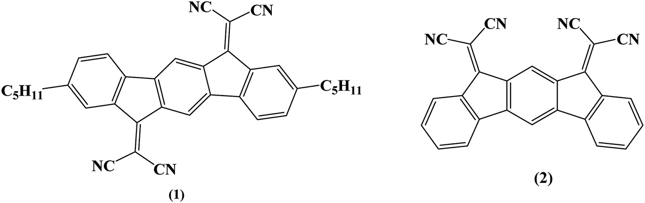 | ||
| Fig. 1 Molecules investigated in this work based either on a dihydroindeno[1,2-b]fluorenyl core (1) or a dihydroindeno[2,1-b]fluorenyl core (2). | ||
Chemistry
Dihydroindenofluorene positional isomers are a class of appealing organic semiconductors consisting of three bridged phenyl units and have been widely studied in the last few years.24,25 In the field of organic electronics, they have found promising applications as high triplet host materials in Phosphorescent Organic Light Emitting Diodes (PhOLEDs),26–29 as blue emitters in OLEDs,30–35 in solar cells36,37 and as n-type semiconductors in OFETs.38–45 In this work, the new semiconductor (1) is constructed on the association of a 6,12-dihydroindeno[1,2-b]fluorene core, possessing on the bridges electron-withdrawing dicyanovinylene fragments. These fragments are known to strongly depress the LUMO energy level of the π-system bearing them.17,41,46 In addition, pentyl side chains have been introduced on the C2 and C8 carbon atoms of the dihydroindeno[1,2-b]fluorene core. For comparison purposes, another dihydroindenofluorene positional isomer (10,12-dihydroindeno[2,1-b]fluorene) previously described in the literature has also been investigated herein (molecule (2)).‡41 There are two structural differences between (1) and (2). The first is the geometry, where (2) has the two dicyanovinylene units on the same side of the dihydroindeno[2,1-b]fluorenyl backbone, whereas in (1) they are on two opposite sides of the dihydroindeno[1,2-b]fluorenyl core. The second difference is the presence of pentyl side chains in (1). These two parameters seem to have a crucial role in the performance and stability of the present OFETs as investigated below.The synthesis of (1) starts with the Suzuki–Miyaura cross-coupling of diethyl 2,5-dibromoterephthalate (3)47 with commercially available 4-pentylphenylboronic acid (Pd(PPh3)4, K2CO3, THF/H2O) providing the corresponding terphenyl (5) with the ester groups on the central phenyl ring and in the ortho position of one phenyl unit (Scheme 1, top). Acid promoted (MeSO3H) intramolecular Friedel–Crafts acylation23,48 of (5) at high temperature (120 °C) readily took place to give the 2,8-dipentylindeno[1,2-b]fluorene-6,12-dione (6) with 86% yield. It should be noted that (6) is soluble in common organic solvents and is more soluble than its non-substituted analogue indeno[1,2-b]fluorene-6,12-dione, previously reported in literature.49 With dione (6) in hand, a Knoevenagel condensation in the presence of malononitrile and pyridine was finally performed providing bisdicyanovinylene (1) with a good yield of 59% (see the Experimental section for synthetic details). One should note that this reaction does not use titanium tetrachloride, a Lewis acid frequently used to activate the carbonyl units in such a reaction.46,50 This route is easy to perform, efficient (overall yield of 43%) and allows a gram scale preparation of (1), which is a key feature for further device applications. The synthesis of (2) is based on a similar strategy from diethyl 4,6-dibromoisophthalate 7 and has previously been reported (Scheme 1, bottom).41
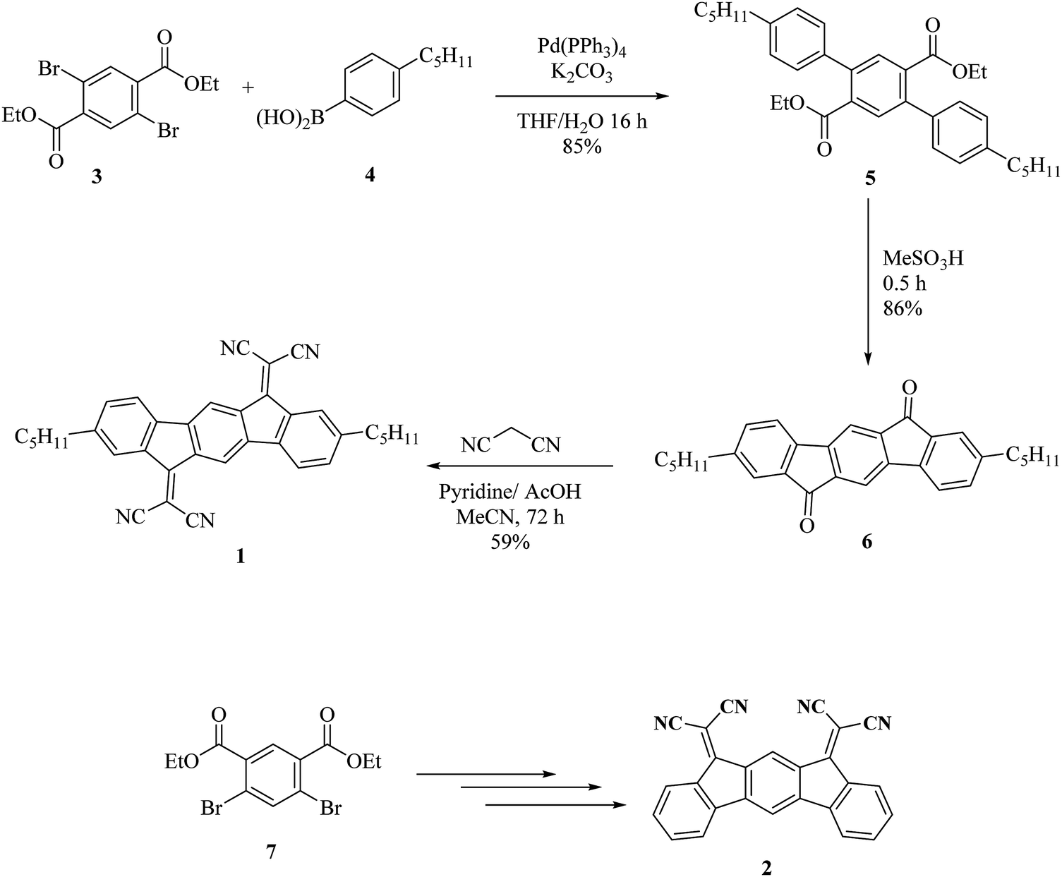 | ||
| Scheme 1 Synthesis of (1) and (2). | ||
The determination of the LUMO energy level was of particular interest for the purpose of this work based on n-type OFETs as a low LUMO energy level is a key feature for charge injection within such a device. The LUMO can be estimated by means of cyclic voltammetry as LUMO (eV) = −[Eredonset (vs. SCE) + 4.4] (based on an SCE energy level of 4.4 eV relative to the vacuum), Fig. 2.51,52 In dichloromethane, the voltammogram of (1) displays two reversible waves with maxima recorded at −0.42 and −0.64 V vs. SCE. Thus, the LUMO energy level of (1) has been estimated at ca. −4.1 eV (Eonset = −0.30 V). This value appears to be very deep, highlighting the strong impact of the dicyanovinylene units on the dihydroindeno[1,2-b]fluorenyl core.53 As the LUMO level of (2) has been reported at −3.81 eV, one should note that it is lowered by 0.30 eV compared to that of (1). This difference can be assigned to the structural deformations of the π-conjugated core of (2).41
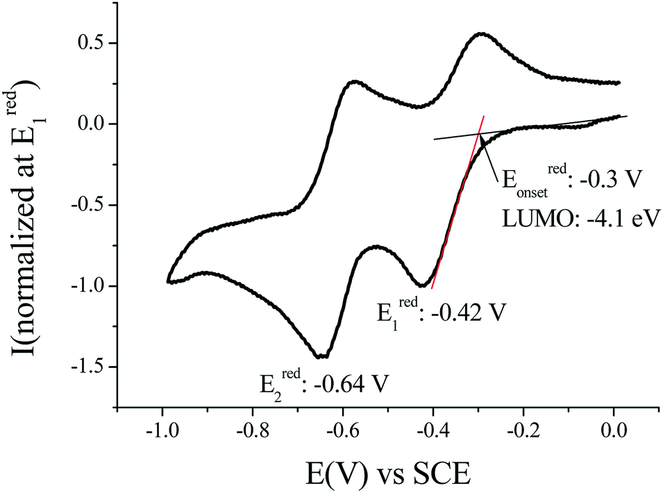 | ||
| Fig. 2 Cyclic voltammetry at 0.1 V s−1 in CH2Cl2/[NBu4][PF6] 0.2 M in the presence of (1) and a platinum disk working electrode. | ||
Organic field-effect transistors
Compounds (1) and (2) were investigated through the fabrication and electrical characterization of bottom-gate bottom-contact n-type channel OFETs in which they were used as the active layer (see the OFET structure and fabrication process in the experimental part). The SU8 photoresist, used as the insulator, participates in the final goal to realize fully organic devices.17 Moreover, as the surface morphology of the gate dielectric affects the semiconductor layer growth, the solution processed insulator remains the best way to ensure a smooth interface between these layers.Transfer characteristics in the linear (VDS = 10 V) and saturation (VDS = 100 V) regimes of (1) and (2) based OFETs are presented in Fig. 3. The most important parameters, that is, the mobility μFE, the threshold voltage (VTH), the subthreshold swing (SS), and the on/off values of the drain current ID (IDon/IDoff) were extracted from the transfer characteristics in the linear and saturated regime and are gathered in Table 1.
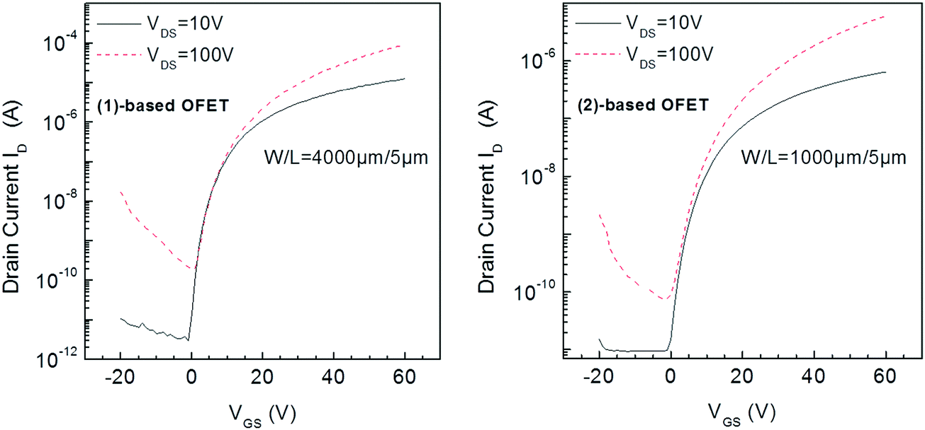 | ||
| Fig. 3 Transfer characteristics in the linear (VDS = 10 V) and saturation (VDS = 100 V) regimes of (1)-based OFETs (left) and (2)-based OFETs (right). | ||
| Molecule | Regime | μ FE (cm2 V−1 s−1) | V TH (V) | SS (V dec−1) | I Don/IDoff |
|---|---|---|---|---|---|
| (1) | Linear | 0.005 | 26 | 1.3 | 4 × 10⁶ |
| Saturation | 0.021 | 20 | 1.9 | 5 × 10⁵ | |
| (2) | Linear | 0.0009 | 20 | 2.3 | 8 × 10⁴ |
| Saturation | 0.002 | 17 | 3.2 | 7 × 10⁴ | |
The threshold voltage values are similar for both OFETs, typically around 20 V. This value can, nevertheless, be considered as high. However, it is clear that both OFETs can operate at a lower voltage. Indeed, all previous parameters have been determined from the classical equations of MOSFETs (Metal Oxide Semiconductor Field-Effect Transistor), see eqn (4)–(7) in the experimental section. Although these equations are used for OFETs and more generally for disordered semiconductor-based transistors, they were initially established for single crystalline silicon MOSFETs. However, in MOSFETs, the swing off–on is very sharp with a subthreshold slope SS value below 100 mV dec−1. For disordered material based FETs, the swing is very slow leading to operational transistors in the subthreshold regime. In other words, OFETs studied in this work could be polarized at values below the threshold voltage value.
The field-effect electron mobility of (1)-based OFETs in saturation was found to be 0.02 cm2 V−1 s−1, being 10 times higher than that of (2)-based OFETs (0.002 cm2 V−1 s−1). The value found for (1) appears to be interesting for a dihydroindenofluorene but remains lower than those recently reported for indeno[1,2-b]fluorenones bearing either S-butyl side chains (0.65 cm2 V−1 s−1)42 or thiophene units (0.12 cm2 V−1 s−1)44 with different device architectures. One can also note that the IDon/IDoff ratio is significantly higher for (1)-based OFETs compared to (2)-based OFETs both in the linear and saturation regimes (Table 1). These IDon/IDoff values obtained for (1)-based OFETs (4 × 10⁶) appear promising for practical applications. Finally, the SS value of (1)-based OFETs (1.3 V dec−1 in the linear regime) is also appealing for circuits and again appear to be better than that of (2)-based OFETs (2.3 V dec−1). The electrical quality of the insulator–semiconductor interface can be involved in the good SS value. All these features clearly highlight that switching from the syn geometry found in the previously reported dihydroindeno[2,1-b]fluorene core of (2) to an anti geometry in the present dihydroindeno[1,2-b]fluorene core of (1) coupled to the addition of pentyl side chains have beneficial effects on both the field-effect mobility, the IDon/IDoff ratio and the SS without negative consequences on VTH.
It should be mentioned that the groups of Marks and Fachetti have reported a structurally related dicyanovinylene-dihydroindeno[1,2-b]fluorene semiconductor possessing dodecanyl chains on the central phenyl ring. This compound did not possess any FET activity.39 Thus, the shortening of the alkyl chains (from C12 to C5) and their shifts to the side phenyl rings has an impressive beneficial effect on the field-effect mobility.
It is important to stress that the present OFET structure (i) is nearly fully organic-based with only the electrodes made in an inorganic material and (ii) has no particular treatment on the electrode surface or on the gate insulator (before deposition of the active layer). With device engineering (such as the grafting of self-assembled monolayers of 4-(dimethylamino)benzenethiol on the electrodes as previously reported on structurally related semiconductors),17 we are convinced that the present performance of (1)-based OFETs can be increased in future work.
Although the mobility, the subthreshold slope, the threshold voltage and the IDon/IDoff ratio provide interesting information to compare organic semiconductors in an OFET, they are not sufficient to perfectly understand their behaviour in a circuit. The behaviour of the active layer under polarization is therefore crucial to further achieve a circuit and the electrical stability of OFETs is one of the central parameters for practical use.
We first focus on the electrical behaviour of OFETs under a low (VGSstress − VTH = 20 V, Fig. 4-bottom) and a high (VGSstress − VTH = 40 V, Fig. 4-top) gate bias stress, both being higher than the threshold voltage. This experiment, called gate bias stress, involves applying a high bias voltage on the gate electrode to maintain the OFET in the on-regime. The stress voltage is applied for a total duration of 3 hours. Drain and source electrodes are grounded in order to uniformly stress the channel. At regular intervals of time, the stress is removed and transfer characteristics are plotted.
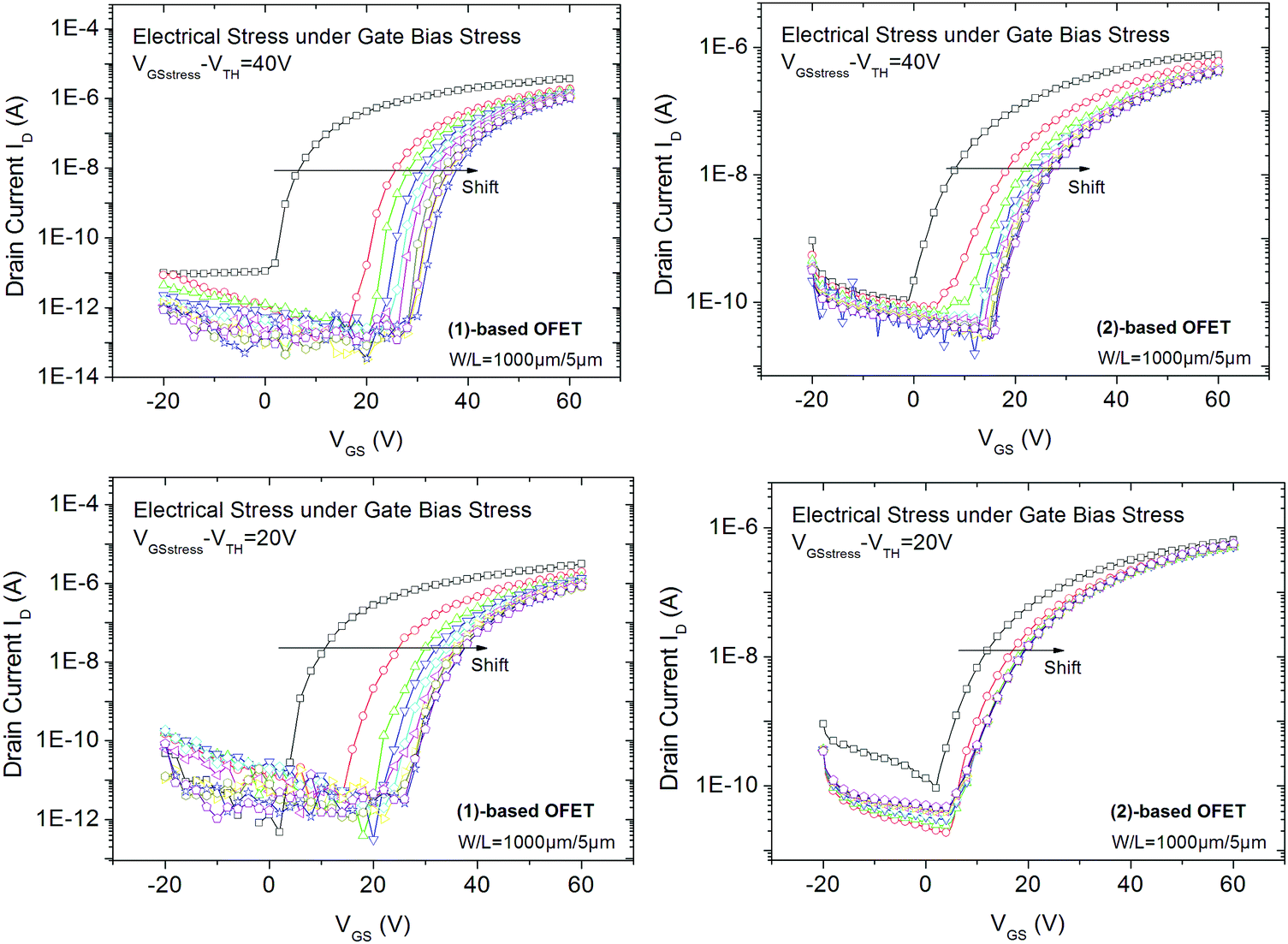 | ||
| Fig. 4 Transfer characteristics of (1) and (2)-based OFETs recorded at different times (every 20 minutes) of gate bias stress for VGSstress − VTH = 40 V (top) and for VGSstress − VTH = 20 V (bottom). | ||
For all experiments, we first note a significant shift in the threshold voltage (ΔVTH) toward positive values (Fig. 4). This is a classical behaviour.20 ΔVTH reaches its highest value during the first 20 minutes of stress and then gradually decreases.
At VGSstress − VTH = 40 V, we note for both OFETs that the maximum current (at VGS = 60 V) decreases with the stress time whereas the threshold voltage increases (Fig. 4). For the (2)-based OFET, the maximum current decreases by 40% and the threshold voltage increases by 60%. Both variations are larger for (1)-based OFET. As the current decreases by 70% and the threshold voltage increases by 100%, from a molecular point of view, we hypothesize that the difference between the two molecules can be ascribed to the alkyl chains borne by (1). However, these gate bias stress effects deserve to be discussed in detail, see below.
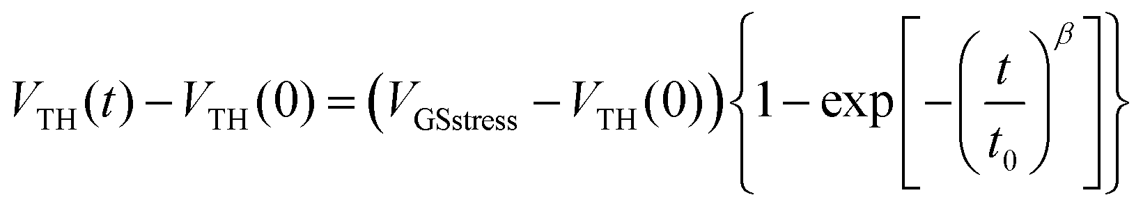
At VGSstress − VTH = 20 V (Fig. 4, bottom), the same conclusions as those above exposed for VGSstress − VTH = 40 V can be drawn for both OFETs with a striking difference: ΔVTH is strongly attenuated in the case of 2 whereas ΔVTH remains almost identical in the case of 1. Thus, we note a different VTH shift as a function of the stress applied. This led us to more precisely investigate this feature. Two different mathematical models (eqn (1) and (2)) are used herein to understand the gate bias stress variations presented above: a stretched exponential law (eqn (1)), which implies a defect density creation54 within the organic semiconductor and a charge carrier trapping law (eqn (2)) occurring inside the gate insulator.55
In the case of defect density creation, the VTH variation with the stress time t is described by a stretched exponential law:
 | (1) |
The stretched exponential law is usually involved in describing relaxation phenomena in glasses towards equilibrium under different stresses.56 This law was established considering a diffusion of specific particles in a material with randomly distributed energy states. These states are able to trap these particles (‘trapping sites’).57 In disordered materials, containing metastable states, some physical parameters such as conductivity,58 threshold voltage of FETs54 or magnetization56 evolve following a stretched exponential law. In amorphous silicon TFTs, this effect has been associated with a dispersive diffusion coefficient of atomic hydrogen.54 This dispersion comes from the nature of any disordered material in which the trapping sites present a distribution of energy states. The β parameter in eqn (1) is related to this distribution of states and to the temperature. Most of the time, this law is efficient for describing the effect of any applied stress in a wide panel of situations. In single crystalline silicon-based MOSFET59 and polycrystalline silicon TFTs, the VTH shift is related to the disordered gate insulator/active layer interface. In this case, the dispersive diffusion within the gate insulator/active layer interface (disordered material) can be involved. In disordered materials in general, any energy absorption inducing new charge carrier distribution can change the state of the weakest bonds, thus disturbing the equilibrium. The deformation can diffuse through the material leading to a new equilibrium state characterized by new defect distribution.
To explain the effect of the gate bias stress, another explanation involves a charge carrier trapping inside the gate insulator.55 This carrier trapping can be negligible in most OFETs that use inorganic silicon dioxide as the gate insulator. However, since the present gate insulator is an organic material i.e. SU8 photoresist, the trapping model deserves to be precisely investigated. This model involves an injection of carriers inside the insulator due to the applied gate bias stress. These carriers are trapped inside the insulator, fixing an electrical charge, which creates an opposite electric field near to the channel. Consequently, the effective gate voltage changes and induces the charge accumulation in the channel, leading to drain current variation. The threshold voltage variation is described by a logarithmic stress time dependence:55
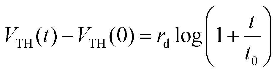 | (2) |
In order to investigate which model can be used in the present case, two values for gate bias stress (VGSstress − VTH = 20 V or 40 V) and two different temperatures (30 and 40 °C) for both (1)- and (2)-based OFETs were investigated. The purpose is to favour the defect density creation and to evaluate the effect of the stress temperature.
We first started with a stress applied on the known compound (2) at a low-stress voltage, VGSstress − VTH = 20 V and for 2 different temperatures, 30 °C and 40 °C (Fig. 5a). The threshold voltage behaviour of these OFETs during the stress was successfully fitted by the stretch exponential model, i.e., eqn (1), describing the defect density creation (correlation factors are 0.995 and 0.991 at 30 °C and 40 °C respectively). The values obtained (β = 0.18 and t0 = 5.5 × 10³ s at 30 °C and β = 0.28 and t0 = 2 × 10³ s at 40 °C) appear to be similar to those reported in literature for amorphous silicon FETs;61 as expected, β increases and t0 decreases with the temperature. The maximum VTH shift increases with the temperature, which is a coherent feature since trapping is enhanced when a higher density of carriers is generated in the channel. One can conclude that the stretch exponential model is suitable for the present stress and the VTH shift could be attributed to defect density creation in the active layer. However, fitting the same experimental curves, with eqn (2) corresponding to the trapping model, attenuates this assignment. Indeed, Fig. 5b shows the same experimental curves as those presented in Fig. 5a but fitted with the trapping law (eqn (2)). It is clear that both experimental curves at 30 and 40 °C are also well fitted by this relation, with rd = 3.82 and t0 = 0.4 s at 30 °C and rd = 5.7 and t0 = 3.3 s at 40 °C (correlation factors are 0.995 and 0.992 at 30 °C and 40 °C respectively).
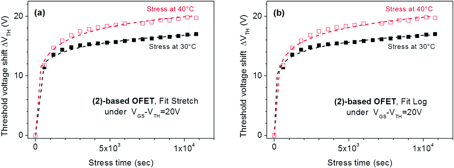 | ||
| Fig. 5 Evolution of ΔVTH with the stress time for (2)-based OFETs under VGSstress − VTH = 20 V at 30 °C and 40 °C. (a) The dashed lines are the fit with stretched exponential eqn (1). (b) The dashed lines are the fit with logarithmic eqn (2). | ||
To conclude, both experimental curves were well fitted by both the eqn (1) and (2), describing respectively the defect density creation inside the active layer and the carrier trapping at the gate insulator. The correlation coefficients are nearly the same. This fit alone does not allow discrimination between the two models and a possible explanation is that both phenomena simultaneously occur in the present stress conditions. This statement has also been observed when using different insulator layers to understand the dominant effect of threshold voltage shift.62
Interestingly, the investigations of (1)-based OFETs in identical experimental conditions (VGSstress − VTH = 20 V) provide very different results. Indeed, attempts to fit the VTH shift with the stretched exponential law (eqn (1)) failed and on the contrary, the fit with trapping law (eqn (2)) succeeded (Fig. 6a). The correlation factor is 0.996 and the parameters rd and t0 are 10.7 and 28.8 s respectively at T = 30 °C. One can, therefore, conclude that the instability of (1)-based OFETs under low gate bias stress arises from carrier trapping occurring inside the gate insulator. This is a different behaviour from that exposed above for (2).
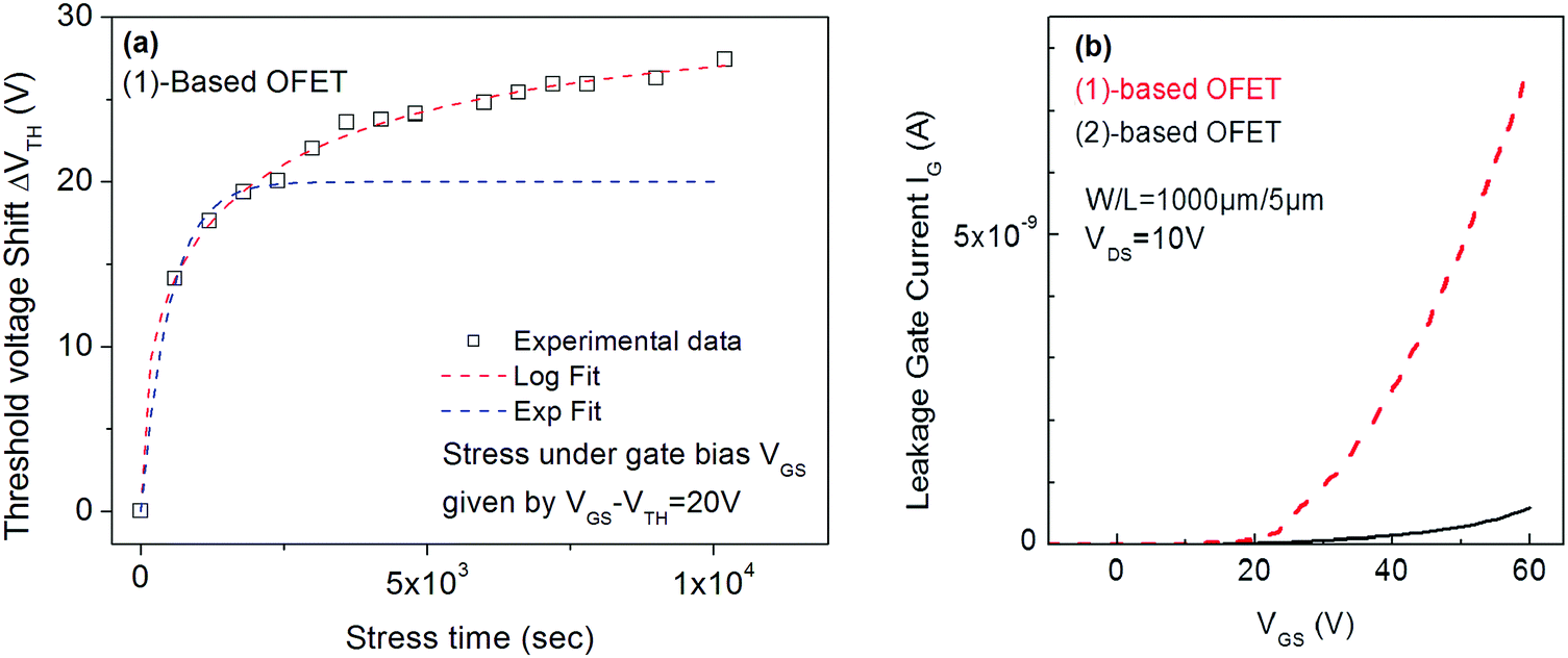 | ||
| Fig. 6 (a) VTH shift with the stress time under VGSstress − VTH = 20 V for (1)-based OFETs. Red dashed lines correspond to fit with logarithmic eqn (2) and blue dashed lines correspond to fit with stretched-exponential eqn (1). (b) Gate leakage current in (1) and (2)-based OFET. | ||
In conclusion, under low gate bias stress (20 V), the VTH shift of (2)-based OFETs seems to be due to both the defect density creation inside the active layer and the carrier trapping inside the gate insulator. On the contrary, the VTH shift of (1)-based OFET seems to be entirely due to the carrier trapping in the insulator. This indicates not only the better stability of the semiconductor (1) under electrical stress but more importantly, a very different trapping behaviour compared to its structural analogue (2). This observation could be argued based on a higher gate leakage current in (1)-based OFETs (Fig. 6b) compared to (2)-based OFETs, increasing the probability to trap charges in the insulator. From a molecular point of view, switching from syn geometry in 2 to anti geometry in 1 and introducing pentyl side chains has significantly changed the origin of the OFETs electrical instabilities. The origins of these electrical instabilities come from a different insulator/semiconductor interface. This work shows how slight structural modifications of the molecular structure of the semiconductor can lead to different insulator/semiconductor interfaces and thus to electrical instabilities arising from different features. Interface effects on the electrical instabilities have previously been approached by Ahmed et al.63,64
In a second step, similar studies were performed by increasing the gate bias stress (VGSstress − VTH = 40 V) of (1) and (2)-based OFETs. The goal was to investigate the influence of the gate bias stress on the origin of the instabilities. This should lead to prominent trapping as tunnelling phenomena such as Fowler–Nordheim tunnelling generally occur at high applied voltage.57 For both (1) and (2)-based OFETs, the experimental curves are well-fitted (Fig. 7a) exclusively by eqn (2) and not by eqn (1). One can, therefore, conclude that at a high-stress voltage, the VTH shift of both (1) and (2)-based OFETs follow the same trapping law.
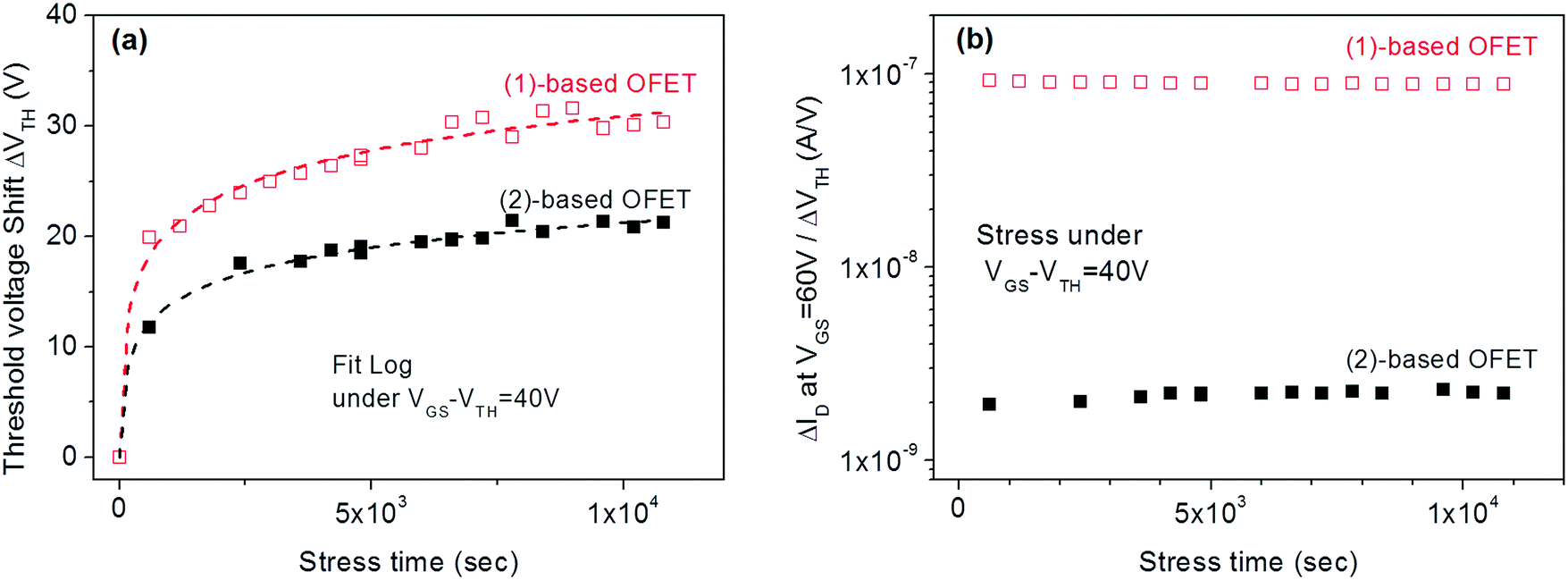 | ||
Fig. 7 (a) VTH shift with the stress time for (1) and (2)-based OFETs under VGSstress − VTH = 40 V. The dashed lines correspond to the fit with logarithmic eqn (2). (b) The  ratio is a function of stress time for (1) and (2)-based OFETs under VGSstress − VTH = 40 V. ratio is a function of stress time for (1) and (2)-based OFETs under VGSstress − VTH = 40 V. | ||
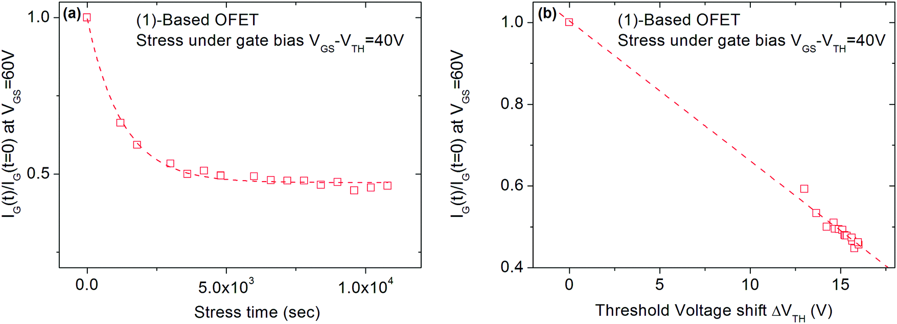
In order to highlight this phenomenon, the ratio between the current variation and the VTH shift is plotted in Fig. 7b as a function of the stress time for both OFETs. At constant VGS, fixed at 60 V, and constant VDS, fixed at 10 V, the ratio of current variation to threshold voltage shift is given by the following:
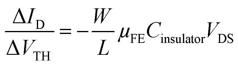 | (3) |
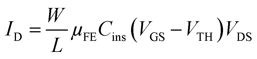
Finally, the VTH shift difference between (1) and (2)-based OFETs should be explained. As mentioned above, the VTH increases by 100% for (1)-based OFETs and only by 60% for (2)-based OFETs after 3 hours of VGSstress − VTH = 40 V stress (Fig. 4). To explain the difference, the phenomenon of charge injection through tunnelling effects responsible for the carrier trapping can be involved. Here, the injected current is the leakage gate current IG in the gate insulator. The variation of the trapped charges ΔQ is proportional to the injected current in the insulator. Due to the screening of previously trapped charges, the injected current decreases during the stress. The variation of these trapped charges is found to be responsible for the VTH shift (ΔVTH = −ΔQ/Cinsulator). With this explanation, the gate leakage current is expected to decrease during the gate bias stress. In this case, its decrease is expected to be proportional to VTH shift. Fig. 8 shows the decrease in the gate leakage current with the stress time for (1)-based OFETs. Plotting IG current as a function of VTH shift confirms the linear dependence between these two parameters (Fig. 8b). Therefore, Fig. 8 confirms that the effect of gate bias stress on (1)-based OFETs is due to carrier trapping inside the gate insulator. More generally, we can expect a significant VTH shift depending on the initial value of the gate current in the case where the carrier trapping phenomenon is involved. Thus, the larger VTH shift observed for (1)-based OFETs compared to (2)-based OFETs, under the same gate bias stress, could be explained by the higher gate leakage current initially observed in the device (Fig. 6b).
 | ||
| Fig. 8 (a) Decrease in leakage current IGS (at VGS = 60 V) for (1)-based OFETs during stress time under VGSstress − VTH = 40 V. (b) Linear relationship between IG and VTH for (1)-based OFETs under VGSstress − VTH = 40 V. | ||
Conclusion
In this work, we report our investigations on the electrical stability of n-type OFETs based on electron-poor dihydroindenofluorene derivatives incorporating dicyanovinylene fragments. First, we have shown that the new dihydro[1,2-b]indenofluorene semiconductor (1) presents better OFETs characteristics compared to the previously reported dihydro[2,1-b]indenofluorene semiconductor (2) (higher μFE and IDon/IDoff, lower SS). However, despite better electrical parameters, molecule (1) leads to less stable OFETs than molecule (2), showing that the most efficient device is not always the most stable one. This is an important feature for practical applications of OFETs.More importantly, we have surprisingly shown that the threshold voltage shift of the OFETs based on these two structurally related molecules arise from different features. Indeed, at low gate bias stress, the carrier trapping inside the insulator well explains the instability of (1)-based OFETs, whereas for (2)-based OFETs both the carrier trapping inside the insulator and the defect density creation inside the active layer can be involved. At high gate bias stress, the situation is again different as only the carrier trapping inside the insulator is involved for both (1) and (2)-based OFETs.
In addition, this work has also shown that (1)-based OFET displays a larger VTH shift than (2)-based OFET (under the same gate bias stress), which has been assigned to a higher gate leakage current in the former. This feature can be related to the different insulator/semiconductor interfaces. Thus, this work shows how slight structural modifications of the molecular structure of the semiconductor can induce electrical instabilities of the corresponding OFETs arising from different features.
Experimental section
Synthesis
All manipulations of oxygen- and moisture-sensitive materials were conducted with a standard Schlenk technique. Commercially available reagents and solvents were used without further purification other than those detailed below. THF was distilled from sodium/benzophenone prior to use. Light petroleum refers to the fraction with bp 40–60 °C. Reactions were stirred magnetically, unless otherwise indicated. Analytical thin layer chromatography was carried out using aluminium backed plates coated with Merck Kieselgel 60 GF254 and visualized under UV light (at 254 and 360 nm). Chromatography was carried out using Teledyne Isco CombiFlash® Rf 400 (UV detection 200–360 nm), over standard silica cartridges (Redisep® Isco). 1H and 13C NMR spectra were recorded using Bruker 300 MHz instruments (1H frequency, corresponding 13C frequency: 75 MHz); chemical shifts were recorded in ppm and J values in Hz. In the 13C NMR spectra, signals corresponding to C, CH, CH2 or Me groups, assigned from DEPT, are noted. The residual signals for the NMR solvents are as follows: CDCl3; 7.26 ppm for the proton and 77.00 ppm for the carbon. The following abbreviations have been used for the NMR assignment: s for singlet, d for doublet, t for triplet and m for multiplet.Compound 2 was synthesized according to literature procedures with spectroscopic analyses and purity in accordance with those of our previous works.41 The optical and electrochemical properties of 2 can be found in our previous works.41
Compound 1 was synthesized as presented below.
![[thin space (1/6-em)]](https://www.rsc.org/images/entities/char_2009.gif) :1, 35 ml) under an argon atmosphere. The resulting mixture was degassed and stirred 16 h at 75 °C. The resulting mixture was quenched with a saturated solution of ammonium chloride (20 ml) and extracted with ethyl acetate (2 × 50 ml). The combined extracts were dried over MgSO4, filtered, evaporated in vacuo and purified by column chromatography on silica gel eluting with a gradient of light petroleum–ethyl acetate (100:0 to 95:5) to give the title compound as a colorless solid (0.437 g, 85%). M.p. 92–94 °C (from ethyl acetate) νmax/cm−1 2956, 2942, 2873, 2837, 1714 (CO), 1463, 1274, 1112, 848, 590; 1H NMR (300 MHz; CDCl3) δ 7.80 (2H, s, Ar-
:1, 35 ml) under an argon atmosphere. The resulting mixture was degassed and stirred 16 h at 75 °C. The resulting mixture was quenched with a saturated solution of ammonium chloride (20 ml) and extracted with ethyl acetate (2 × 50 ml). The combined extracts were dried over MgSO4, filtered, evaporated in vacuo and purified by column chromatography on silica gel eluting with a gradient of light petroleum–ethyl acetate (100:0 to 95:5) to give the title compound as a colorless solid (0.437 g, 85%). M.p. 92–94 °C (from ethyl acetate) νmax/cm−1 2956, 2942, 2873, 2837, 1714 (CO), 1463, 1274, 1112, 848, 590; 1H NMR (300 MHz; CDCl3) δ 7.80 (2H, s, Ar-![[H with combining low line]](https://www.rsc.org/images/entities/char_0048_0332.gif) ), 7.30–7.27 (4H, d, J 8.1, Ar-), 7.24–7.21 (4H, d, J 8.1, Ar-), 4.16–4.08 (4H, q, J 7.5, OC2Me), 2.68–2.63 (4H, t, J 7.5, Ar-C2CH2), 1.69–1.64 (4H, m, J 7.5, Ar-CH2C2), 1.38–1.35 (8H, m, C2), 1.04–0.99 (6H, t, J 7.5, OCH2
), 7.30–7.27 (4H, d, J 8.1, Ar-), 7.24–7.21 (4H, d, J 8.1, Ar-), 4.16–4.08 (4H, q, J 7.5, OC2Me), 2.68–2.63 (4H, t, J 7.5, Ar-C2CH2), 1.69–1.64 (4H, m, J 7.5, Ar-CH2C2), 1.38–1.35 (8H, m, C2), 1.04–0.99 (6H, t, J 7.5, OCH2![[M with combining low line]](https://www.rsc.org/images/entities/char_004d_0332.gif)
![[e with combining low line]](https://www.rsc.org/images/entities/char_0065_0332.gif) ), 0.94–0.89 (6H, t, J 7.5, CH2); 13C NMR (75 MHz, CDCl3) δ 168.3 (CO), 142.4 (C), 140.8 (C), 137.4 (C), 133.5 (CH), 131.7 (CH), 128.3 (CH), 128.2 (CH), 61.2 (CH2), 35.6 (CH2), 31.5 (CH2), 31.1 (CH2), 22.5 (CH2), 14.0 (CH3), 13.7 (CH3).
), 7.43 (2H, s, Ar-), 7.38–7.35 (2H, d, J 7.8, Ar-), 7.30–7.28 (2H, dd, J 7.5, 1.5, Ar-), 2.62–2.57 (4H, t, J 7.5, Ar-C2CH2), 1.66–1.56 (4H, m, J 7.5, Ar-CH2C2), 1.34–1.24 (8H, m, C2), 0.92–0.87 (6H, t, J 7.5, CH2); 13C NMR (75 MHz, CDCl3) δ 192.5 (CO), 144.9 (C), 144.1 (C), 140.45 (C), 138.6 (C), 134.5 (C), 133.5 (CH), 123.7 (CH), 119.6 (CH), 114.8 (CH), 35.0 (CH2), 30.6 (CH2), 30.0 (CH2), 21.7 (CH2), 13.2 (CH3). UV-vis (CH2Cl2) [λmax/nm (ε in L mol−1 cm−1)] = 295 (1.48 × 10⁵), 285.5 (17.4 × 10⁴), 269 (3.0 × 10⁴).
), 8.16 (2H, s, Ar-), 7.53–7.50 (2H, d, J 7.8, Ar-), 7.37–7.34 (2H, dd, J 7.5, 1.5, Ar-), 2.68–2.62 (4H, t, J 7.5, Ar-C2CH2), 1.65–1.60 (4H, m, Ar-CH2C2), 1.34–1.30 (8H, m, C2), 0.89–0.85 (6H, t, J 7.5, CH2). UV-vis (CH2Cl2) [λmax/nm (ε in L mol−1 cm−1)] = 403 (1.85 × 10⁴), 382.5 (1.90 × 10⁴), 319 (5.4 × 10⁴), 305.5 (8 × 10⁴).
), 0.94–0.89 (6H, t, J 7.5, CH2); 13C NMR (75 MHz, CDCl3) δ 168.3 (CO), 142.4 (C), 140.8 (C), 137.4 (C), 133.5 (CH), 131.7 (CH), 128.3 (CH), 128.2 (CH), 61.2 (CH2), 35.6 (CH2), 31.5 (CH2), 31.1 (CH2), 22.5 (CH2), 14.0 (CH3), 13.7 (CH3).
), 7.43 (2H, s, Ar-), 7.38–7.35 (2H, d, J 7.8, Ar-), 7.30–7.28 (2H, dd, J 7.5, 1.5, Ar-), 2.62–2.57 (4H, t, J 7.5, Ar-C2CH2), 1.66–1.56 (4H, m, J 7.5, Ar-CH2C2), 1.34–1.24 (8H, m, C2), 0.92–0.87 (6H, t, J 7.5, CH2); 13C NMR (75 MHz, CDCl3) δ 192.5 (CO), 144.9 (C), 144.1 (C), 140.45 (C), 138.6 (C), 134.5 (C), 133.5 (CH), 123.7 (CH), 119.6 (CH), 114.8 (CH), 35.0 (CH2), 30.6 (CH2), 30.0 (CH2), 21.7 (CH2), 13.2 (CH3). UV-vis (CH2Cl2) [λmax/nm (ε in L mol−1 cm−1)] = 295 (1.48 × 10⁵), 285.5 (17.4 × 10⁴), 269 (3.0 × 10⁴).
), 8.16 (2H, s, Ar-), 7.53–7.50 (2H, d, J 7.8, Ar-), 7.37–7.34 (2H, dd, J 7.5, 1.5, Ar-), 2.68–2.62 (4H, t, J 7.5, Ar-C2CH2), 1.65–1.60 (4H, m, Ar-CH2C2), 1.34–1.30 (8H, m, C2), 0.89–0.85 (6H, t, J 7.5, CH2). UV-vis (CH2Cl2) [λmax/nm (ε in L mol−1 cm−1)] = 403 (1.85 × 10⁴), 382.5 (1.90 × 10⁴), 319 (5.4 × 10⁴), 305.5 (8 × 10⁴).
Electrochemical studies
Electrochemical experiments were performed under an argon atmosphere, using a Pt disk electrode (diameter 1 mm), the counter electrode was a vitreous carbon rod and the reference electrode was a silver wire in a 0.1 M AgNO3 solution in CH3CN. Ferrocene was added to the electrolytic solution at the end of a series of experiments. The ferrocene/ferrocenium (Fc/Fc+) couple served as internal standard. The three-electrode cell was connected to a PAR Model 273 potentiostat/galvanostat (PAR, EG&G, USA) monitored with the ECHEM Software. Activated Al2O3 was added in the electrolytic solution to remove excess moisture. All potentials are referred to the SCE electrode that was calibrated at 0.405 V vs. the Fc/Fc+ system. Following the work of Jenekhe, we estimated the electron affinity (EA) or lowest unoccupied molecular orbital (LUMO) from the redox data. The LUMO level was calculated from: LUMO (eV) = −[Eredonset (vs. SCE) + 4.4] based on an SCE energy level of 4.4 eV relative to the vacuum.51,52OFETs fabrication and characterization
Bottom gate-bottom contact transistors were fabricated on glass substrates. Substrates were previously cleaned with acetone and rinsed with ethanol. An aluminium layer of 150 nm was then deposited by thermal evaporation and wet-etched to define gate electrodes. 320 nm thick SU-8 photoresist (from Microchem) was spin-coated and then exposed to UV light to define the gate insulating layer (see MicroChem Su-8 2000 Permanent Epoxy Negative Photoresist Processing Guidelines for Su-8 2000.5, Su-8 2002, So-8 2005, Su-8 2007, Su-8 2010 and Su-8 2015-http://www.microchem.com/pdf/SU-82000DataSheet2000_5thru2015Ver4.pdf). Then, 60 nm thick gold film was thermally evaporated and then wet-etched to form source and drain electrodes. Finally, the active layer was deposited by thermal evaporation under a high vacuum of 3 × 10⁻⁷ mbar. The substrate temperature was kept constant (Tsub = 30 °C), deposition rate and layer thickness were fixed to 0.4 Å s−1 and 8 nm respectively. After fabrication, a post-annealing treatment on both devices at 110 °C during 90 min under nitrogen ambience was performed.Devices were stored and characterized in a glove box under ambient nitrogen. All electrical characterizations were performed using a Keithley 2636A. Transfer characteristic ID–VGS were plotted at room temperature. All the measurements were made under the same conditions, the gate-source voltage VGS was varied from −20 V to 60 V with a 0.5 V step, at constant drain–source voltage VDS (+10 V or +100 V). The procedure allows us to plot the transfer characteristics in linear and in saturation regimes.
Electrical parameters of both OFETs types in linear and saturation regimes have been summarized in Table 1. As usual, equations for MOSFETs have been used in both regimes. The drain current ID in linear regime (VDS ≪ VGS − VTH) is given by
 | (4) |
 | (5) |
The threshold voltage VTH is the gate voltage axis intercept of ID–VGS curve plotted in linear representation. The field-effect mobility μFE is deduced from the extraction of gm. The given value in Table 1 is the maximum value of μFE. The sub-threshold swing SS was extracted from the ID–VGS curve plotted in the semi-logarithmic scale using relation 6.
 | (6) |
In the saturation regime (VDS ≫ VGS − VTH), the drain current is given by
 | (7) |
In this case, the slope of the square root of ID as a function of VGS, WμFECins/L, will give the mobility μsat in the saturation regime. The threshold voltage VTH is the gate voltage axis intercept of the ID1/2–VGS curve.
Conflicts of interest
There are no conflicts to declare.Acknowledgements
This work is supported by the European Union through the European Regional Development Fund (ERDF), the Ministry of Higher Education and Research, the Région Bretagne, the Département d'Ille et Vilaine and Rennes Metropole, through the CPER Project 2015–2020 MATECOM-ORGAFLEX. The authors wish to thank the C.R.M.P.O. (Rennes) for mass analysis. CP wishes to thank the UMR CNRS 6226-Institut des Sciences Chimiques de Rennes for an ‘Inter UMR’ grant, Dr Maxime Romain for his help and Prof. B. Frontana Uribe (UNAM Mexico). EJ wishes to thanks the IETR for financial support.References
- H. Sirringhaus, Adv. Mater., 2014, 26, 1319–1335 CrossRef PubMed.
- J. T. E. Quinn, J. Zhu, X. Li, J. Wang and Y. Li, J. Mater. Chem. C, 2017, 5, 8654–8681 RSC.
- X. Gao and Y. Hu, J. Mater. Chem. C, 2014, 2, 3099–3117 RSC.
- K. Zhou, H. Dong, H.-L. Zhang and W. Hu, Phys. Chem. Chem. Phys., 2014, 16, 22448–22457 RSC.
- Y. Xu, C. Liu, D. Khim and Y.-Y. Noh, Phys. Chem. Chem. Phys., 2015, 17, 26553–26574 RSC.
- Y. Yuan, G. Giri, A. L. Ayzner, A. P. Zoombelt, S. C. B. Mannsfeld, J. Chen, D. Nordlund, M. F. Toney, J. Huang and Z. Bao, Nat. Commun., 2014, 5, 3005 CrossRef PubMed.
- Z.-H. Wu, Z.-T. Huang, R.-X. Guo, C.-L. Sun, L.-C. Chen, B. Sun, Z.-F. Shi, X. Shao, H. Li and H.-L. Zhang, Angew. Chem., Int. Ed., 2017, 56, 13031–13035 CrossRef PubMed.
- G. Schweicher, V. Lemaur, C. Niebel, C. Ruzié, Y. Diao, O. Goto, W. Y. Lee, Y. Kim, J. B. Arlin, J. Karpinska, A. R. Kennedy, S. R. Parkin, Y. Olivier, S. C. B. Mannsfeld, J. Cornil, Y. H. Geerts and Z. Bao, Adv. Mater., 2015, 27, 3066–3072 CrossRef PubMed.
- J. Liu, H. Zhang, H. Dong, L. Meng, L. Jiang, L. Jiang, Y. Wang, J. Yu, Y. Sun, W. Hu and A. J. Heeger, Nat. Commun., 2015, 6, 10032 CrossRef PubMed.
- F. R. Libsch and J. Kanicki, Appl. Phys. Lett., 1993, 62, 1286–1288 CrossRef.
- T. Sekitani, S. Iba, Y. Kato, Y. Noguchi, T. Someya and T. Sakurai, Appl. Phys. Lett., 2005, 87, 073505 CrossRef.
- D. K. Hwang, C. Fuentes-Hernandez, J. B. Kim, W. J. Potscavage and B. Kippelen, Org. Electron., 2011, 12, 1108–1113 CrossRef.
- D. K. Hwang, K. Lee, J. H. Kim, S. Im, J. H. Park and E. Kim, Appl. Phys. Lett., 2006, 89, 093507 CrossRef.
- C. Goldmann, D. J. Gundlach and B. Batlogg, Appl. Phys. Lett., 2006, 88, 063501 CrossRef.
- H. L. Gomes, P. Stallinga, F. Dinelli, M. Murgia, F. Biscarini, D. M. de Leeuw, T. Muck, J. Geurts, L. W. Molenkamp and V. Wagner, Appl. Phys. Lett., 2004, 84, 3184–3186 CrossRef.
- S. J. Zilker, C. Detcheverry, E. Cantatore and D. M. de Leeuw, Appl. Phys. Lett., 2001, 79, 1124–1126 CrossRef.
- J.-D. Peltier, B. Heinrich, B. Donnio, E. Jacques, J. Rault-Berthelot and C. Poriel, ACS Appl. Mater. Interfaces, 2017, 9, 8219–8232 CrossRef PubMed.
- S. Bebiche, I. Bouhadda, T. Mohammed-Brahim, N. Coulon, J. F. Bergamini, C. Poriel and E. Jacques, Solid-State Electron., 2017, 130, 49–56 CrossRef.
- T. Umeda, D. Kumaki and S. Tokito, Org. Electron., 2008, 9, 545–549 CrossRef.
- R. Häusermann and B. Batlogg, Appl. Phys. Lett., 2011, 99, 083303 CrossRef.
- K. P. Pernstich, S. Haas, D. Oberhoff, C. Goldmann, D. J. Gundlach, B. Batlogg, A. N. Rashid and G. Schitter, J. Appl. Phys., 2004, 96, 6431–6438 CrossRef.
- S. G. J. Mathijssen, M. J. Spijkman, A. M. Andringa, P. A. Van Hal, I. McCulloch, M. Kemerink, R. A. J. Janssen and D. M. de Leeuw, Adv. Mater., 2010, 22, 5105–5109 CrossRef PubMed.
- M. Romain, D. Tondelier, O. Jeannin, B. Geffroy, J. Rault-Berthelot and C. Poriel, J. Mater. Chem. C, 2015, 3, 9701–97014 RSC.
- M. Romain, S. Thiery, A. Shirinskaya, C. Declairieux, D. Tondelier, B. Geffroy, O. Jeannin, J. Rault-Berthelot, R. Métivier and C. Poriel, Angew. Chem., Int. Ed., 2015, 54, 1176–1180 CrossRef PubMed.
- A. G. Fix, D. T. Chase and M. M. Haley, in Topics in Current Chemistry, ed. J. S. Siegel and Y.-T. Wu, Springer, 2014, pp. 159–195 Search PubMed.
- M. Romain, D. Tondelier, B. Geffroy, O. Jeannin, E. Jacques, J. Rault-Berthelot and C. Poriel, Chem. – Eur. J., 2015, 21, 9426–9439 CrossRef PubMed.
- M. Romain, C. Quinton, D. Tondelier, B. Geffroy, O. Jeannin, J. Rault-Berthelot and C. Poriel, J. Mater. Chem. C, 2016, 4, 1692–1703 RSC.
- C. Poriel, R. Métivier, J. Rault-Berthelot, D. Thirion, F. Barrière and O. Jeannin, Chem. Commun., 2011, 47, 11703–11705 RSC.
- L.-C. Chi, W.-Y. Hung, H.-C. Chiu and K.-T. Wong, Chem. Commun., 2009, 3892–3894 RSC.
- M. Romain, D. Tondelier, J.-C. Vanel, B. Geffroy, O. Jeannin, J. Rault-Berthelot, R. Métivier and C. Poriel, Angew. Chem., Int. Ed., 2013, 52, 14147–14151 CrossRef PubMed.
- D. Thirion, M. Romain, J. Rault-Berthelot and C. Poriel, J. Mater. Chem., 2012, 22, 7149–7157 RSC.
- C. Poriel, J. Rault-Berthelot and D. Thirion, J. Org. Chem., 2013, 73, 886–898 CrossRef PubMed.
- C. Poriel, F. Barrière, D. Thirion and J. Rault-Berthelot, Chem. – Eur. J., 2009, 15, 13304–13307 CrossRef PubMed.
- F. Barrière, C. Poriel and J. Rault-Berthelot, Electrochim. Acta, 2013, 110, 735–740 CrossRef.
- K. H. Lee, S. O. Kim, J. N. You, S. Kang, J. Y. Lee, K. S. Yook, S. O. Jeon, J. Y. Lee and S. S. Yoon, J. Mater. Chem., 2012, 22, 5145–5154 RSC.
- J. Kim, S. H. Kim, I. H. Jung, E. Jeong, Y. Xia, S. Cho, I.-W. Hwang, K. Lee, H. Suh, H.-K. Shim and H. Y. Woo, J. Mater. Chem., 2010, 20, 1577–1586 RSC.
- S. Chaurasia, C.-J. Liang, Y.-S. Yen and J. T. Lin, J. Mater. Chem. C, 2015, 3, 9765–9780 RSC.
- H. Usta, A. Facchetti and T. J. Marks, Acc. Chem. Res., 2011, 44, 501–510 CrossRef PubMed.
- H. Usta, C. Risko, Z. Wang, H. Huang, M. K. Deliomeroglu, A. Zhukhovitskiy, A. Facchetti and T. J. Marks, J. Am. Chem. Soc., 2009, 131, 5586–5608 CrossRef PubMed.
- Y.-I. Park, J. S. Lee, B. J. Kim, B. Kim, J. Lee, D. H. Kim, S.-Y. Oh, J. H. Cho and J.-W. Park, Chem. Mater., 2011, 23, 4038–4044 CrossRef.
- M. Romain, M. Chevrier, S. Bebiche, T. Mohammed-Brahim, J. Rault-Berthelot, E. Jacques and C. Poriel, J. Mater. Chem. C, 2015, 3, 5742–5753 RSC.
- Z. P. Fan, X. Y. Li, X. E. Luo, X. Fei, B. Sun, L. C. Chen, Z. F. Shi, C. L. Sun, X. Shao and H. L. Zhang, Adv. Funct. Mater., 2017, 27, 1702318 CrossRef.
- T. Nakagawa, D. Kumaki, J.-I. Nishida, S. Tokito and Y. Yamashita, Chem. Mater., 2008, 20, 2615–2617 CrossRef.
- M. Ozdemir, D. Choi, G. Kwon, Y. Zorlu, H. Kim, M.-G. Kim, S. Seo, U. Sen, M. Citir, C. Kim and H. Usta, RSC Adv., 2016, 6, 212–226 RSC.
- Q. Meng and W. Hu, Phys. Chem. Chem. Phys., 2012, 14, 14152–14164 RSC.
- E. Jacques, M. Romain, A. Yassin, S. Bebiche, M. Harnois, T. Mohammed-Brahim, J. Rault-Berthelot and C. Poriel, J. Mater. Chem. C, 2014, 2, 3292–3302 RSC.
- N. Cocherel, C. Poriel, J. Rault-Berthelot, F. Barrière, N. Audebrand, A. M. Z. Slawin and L. Vignau, Chem. – Eur. J., 2008, 14, 11328–11342 CrossRef PubMed.
- S. Thiery, D. Tondelier, B. Geffroy, O. Jeannin, J. Rault-Berthelot and C. Poriel, Chem. – Eur. J., 2016, 22, 10136–10149 CrossRef PubMed.
- C. Poriel, N. Cocherel, J. Rault-Berthelot, L. Vignau and O. Jeannin, Chem. – Eur. J., 2011, 17, 12631–12645 CrossRef PubMed.
- C. B. Nielsen, E. Voroshazi, S. Holliday, K. Cnops, B. P. Rand and I. Mc Culloch, J. Mater. Chem. A, 2013, 1, 73–76 RSC.
- A. P. Kulkarni, C. J. Tonzola, A. Babel and S. A. Jenekhe, Chem. Mater., 2004, 16, 4556–4573 CrossRef.
- C. M. Cardona, W. Li, A. E. Kaifer, D. Stockdale and G. C. Bazan, Adv. Mater., 2011, 23, 2367–2371 CrossRef PubMed.
- J. Rault-Berthelot, C. Poriel, F. Justaud and F. Barrière, New J. Chem., 2008, 32, 1259–1266 RSC.
- W. B. Jackson, J. M. Marshall and M. D. Moyer, Phys. Rev. B: Solid State, 1989, 39, 1164–1179 CrossRef.
- M. J. Powell, Appl. Phys. Lett., 1983, 43, 597–599 CrossRef.
- R. V. Chamberlin, J. Appl. Phys., 1985, 57, 3377–3381 CrossRef.
- P. Grassberger and I. Procaccia, J. Chem. Phys., 1982, 77, 6281–6284 CrossRef.
- R. Meaudre, M. Meaudre, P. Jensen and G. Guiraud, Philos. Mag. Lett., 1988, 57, 315–320 CrossRef.
- K. O. Jeppson and C. M. Svensson, J. Appl. Phys., 1977, 48, 2004–2014 CrossRef.
- M. J. Powell, C. Van Berkel and J. R. Hughes, Appl. Phys. Lett., 1989, 54, 1323–1325 CrossRef.
- S. G. J. Mathijssen, M. Cölle, H. Gomes, E. C. P. Smits, B. de Boer, I. McCulloch, P. A. Bobbert and D. M. de Leeuw, Adv. Mater., 2007, 19, 2785–2789 CrossRef.
- R. Ahmed, C. Simbrunner, G. Schwabegger, M. A. Baig and H. Sitter, Org. Electron., 2014, 15, 3203–3210 CrossRef.
- R. Ahmed, A. Kadashchuk, C. Simbrunner, G. Schwabegger, M. A. Baig and H. Sitter, ACS Appl. Mater. Interfaces, 2014, 6, 15148–15153 CrossRef PubMed.
- R. Ahmed, C. Simbrunner, M. A. Baig and H. Sitter, ACS Appl. Mater. Interfaces, 2015, 7, 22380–22384 CrossRef PubMed.
Footnotes |
| † Electronic supplementary information (ESI) available. See DOI: 10.1039/c8qm00193f |
| ‡ Note that the corresponding 2,8-dipentyl-dihydroindeno[2,1-b]fluorene/dicyanovinylene has also been synthesized and studied in the course of this work. The electron mobility has been evaluated at 1.09 × 10⁻⁴ cm2 V−1 s−1 but the corresponding OFET does not present stable transfer characteristics. This instability does not allow the study of these OFETs in detail (see ESI† for the synthesis, properties and incorporation of 2,8-dipentyl-dihydroindeno[2,1-b]fluorene/dicyanovinylene) in OFETs. |
| This journal is © the Partner Organisations 2018 |