DOI:
10.1039/C8QM00047F
(Research Article)
Mater. Chem. Front., 2018,
2, 975-985
6,6′-Diaryl-substituted biazulene diimides for solution-processable high-performance n-type organic semiconductors†
Received
28th January 2018
, Accepted 6th March 2018
First published on 7th March 2018
Abstract
Azulene, a non-benzenoid aromatic hydrocarbon, is a promising building block for constructing organic optoelectronic materials. Herein, a series of 6,6′-diaryl-substituted biazulene diimides (1–5) are designed and synthesized for solution-processable organic semiconductors. These compounds exhibited excellent electron transport properties with fine-tuned molecular energy levels (HOMO: −5.68 to −6.04 eV; LUMO: −3.63 to −3.73 eV). Bottom-gate-top-contact organic field effect transistors (OFETs) based on compounds 1–3 and 5 displayed unipolar n-type semiconducting properties with optimized average electron mobilities of 0.12–0.45 cm2 V−1 s−1, of which the devices based on 2 demonstrated an electron mobility of up to 0.52 cm2 V−1 s−1, the highest electron mobilities for azulene-based organic semiconductors and also among the highest values for solution-processable n-channel OFETs. Devices based on 4 showed ambipolar FET performance with electron and hole mobilities of 0.31 cm2 V−1 s−1 and 0.029 cm2 V−1 s−1, respectively. The ambipolar charge transport behavior of 4 is due to its higher HOMO energy level (−5.68 eV) than the others (−5.78 to −6.04 eV). The excellent electron transport ability of compounds 1–5 might be attributed to the dense molecular packing induced by the dipolar moment of the azulene units as revealed by single crystal analysis. Besides, compounds 2 and 5 were used as electron acceptors for organic photovoltaic devices, and an average power conversion efficiency of about 1.3% was obtained for their respective blend thin films with electron donor PTB7-Th. The results demonstrate that 6,6′-diaryl-substituted biazulene diimides are promising solution-processable n-type organic semiconductors, and the azulene unit has great potential for constructing excellent organic optoelectronic materials.
Introduction
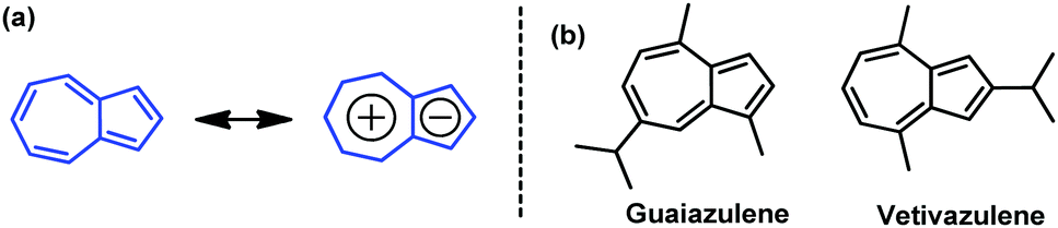
Azulene is a nonbenzenoid aromatic hydrocarbon with beautiful blue color and a large dipole moment of 1.08 D.1 It has attracted particular attention for its unique electronic structure, unusual physical properties and biological activities.2–6 The distinctive character of azulene stems from the fusion of an electron-poor seven-membered ring and an electron-rich five-membered ring (Fig. 1a), affording a “donor–acceptor”-like resonance structure with a non-mirror-related frontier orbital geometry.7–9 This dissimilar electron density distribution between highest occupied molecular orbital (HOMO) and lowest unoccupied molecular orbital (LUMO) endows azulene with a smaller electron repulsion energy in the first excited singlet state and results in a small energy gap.7–9 Azulene derivatives, such as guaiazulene and vetivazulene (Fig. 1b), are constituents of pigments in Lactarius indigo, marine invertebrates, and also guaiac wood oil.10 Guaiazulene can be used as a cosmetic color additive, a component of some skin care products and a drug against ulcers with anti-inflammatory and antiviral properties.10 On the other hand, owing to its novel structure and unique properties, azulene-based compounds have been used for developing advanced organic materials, including conducting polymers,11 nonlinear optical materials,12–15 fluorescence switching materials,16–19 molecular devices,20 electrochromic materials,21 anion receptors/sensors,22 and near-infrared absorption materials.23,24 Recently, azulene was used to construct organic materials for organic field-effect transistors (OFETs)8,9,25–33 as well as solar cells,8,9,34,35 and has attracted more and more attention. These advances highlight the potential of azulene and encourage us to develop novel azulene-based organic semiconductors.
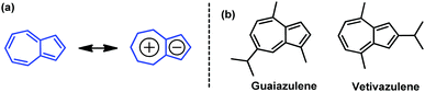 |
| | Fig. 1 (a) Azulene and its resonance structure, and (b) structures of guaiazulene and vetivazulene. | |
In the past decades, organic semiconductors (OSCs) have been receiving ever increasing attention because of their important roles in OFETs, organic photovoltaics (OPVs) and organic light-emitting diodes (OLEDs).36–56 Among them, solution-processable OSCs have become a very important class of candidates to realize flexible, large-area and low-cost organic optoelectronics.36–57 Although much progress on n-channel organic transistors has been made, the performance of solution-processable n-type OSCs has still lagged behind that of their solution-processable p-type counterparts.58–63 To the best of our knowledge, there are few n-type OSCs with mobility >0.5 cm2 V−1 s−1 for solution-processed OFETs.64–70 The exploration of innovative solution-processable n-type OSCs with high device performance is still highly desirable and significant for organic optoelectronics, e.g. organic complementary circuits that exhibit low quiescent power dissipation and high operating speed require both n- and p-type OSCs with comparable performance.71–73 In addition, OSCs with high device performance are usually constructed by traditional aromatic rings such as benzene and thiophene, while the OSCs based on non-traditional conjugated units like azulene are less studied,25–35 leaving much room for studying their unique chemical physical properties and potential applications in organic optoelectronics. Fig. 2 summarizes the electron-transport organic semiconductors based on azulene. AzSQ1 (Fig. 2) was among the first reported azulene-based OSCs that were used in OFETs, and exhibited ambipolar transport characteristics with an electron mobility of about 10−4 cm2 V−1 s−1.25 In 2012, another azulene-based squarylium dye AzSQ2 (Fig. 2) for OFETs was investigated and also showed ambipolar behaviour with electron mobility in the order of 10−4 cm2 V−1 s−1.26 Later on, Katagiri and coworkers synthesized four hydrocarbon oligomers TAz1–TAz4 (Fig. 2) comprising only three azulene units.28,29 Vacuum-deposited OFETs based on TAz2 and TAz3 exhibited ambipolar characteristics with optimized electron mobilities of 4.3 × 10⁻² cm2 V−1 s−1 and 0.31 cm2 V−1 s−1, respectively, whereas TAz1 and TAz4 displayed unipolar n-type transistor behaviors with maximum electron mobilities of 0.29 cm2 V−1 s−1 and 0.15 cm2 V−1 s−1, respectively. In 2016, we designed and synthesized a novel azulene-based aromatic diimide: 2,2′-biazulene-1,1′,3,3′-tetracarboxylic diimide (BAzDI).31 The carbonyl groups were added to the 1- and 3-positions of azulene to obtain deep LUMO energy and the N-alkyl chains are crucial for solution-processed OFETs. The preliminary FET study on a BAzDI derivative showed an electron mobility of 1.5 × 10⁻² cm2 V−1 s−1.31
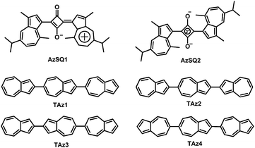 |
| | Fig. 2 Azulene-based electron-transport organic semiconductors. | |
In the previous studies, core modification has been proven to be a viable strategy for controlling molecular packing, tuning the orbital energy levels as well as introducing soluble groups.74,75 Hence, in the present work, we synthesized five new BAzDI derivatives with 2-branched C10,6 alkyl chains and different aryl groups substituted at the 6- and 6′-positions for solution-processed organic semiconductors (Fig. 3). The introduction of aryl groups with different electron-donating/electron-withdrawing abilities at the 6- and 6′-positions of BAzDIs not only fine-tunes the energy levels but also extends the π-conjugated structures which is beneficial for better device performance.75 The spin-coated bottom-gate-top-contact thin film transistors revealed that all of the semiconductors exhibited high electron mobilities (μe,max: 0.15–0.52 cm2 V−1 s−1). Compound 2, with a 4-(trifluoromethyl)phenyl group substituted at the 6- and 6′-positions of BAzDI, displayed the best device performance, with an average electron mobility of about 0.45 cm2 V−1 s−1 and a maximum mobility of up to 0.52 cm2 V−1 s−1, which is the highest electron mobility for azulene-based OSCs and is also among the highest mobility values for solution-processable bottom-gate n-channel OFETs. Interestingly, 6,6′-bis(5-phenylthiophen-2-yl)-substituted BAzDI 4 with appropriate HOMO and LUMO energy levels exhibited ambipolar behavior. In addition, OPV devices with compounds 2 or 5 as the electron acceptor and polymer PTB7-Th as the electron donor provided an average power conversion efficiency (PCE) value of about 1.3%, indicating the potential of aryl-substituted BAzDIs for electron acceptors of OPVs. Our studies suggested that BAzDIs are promising semiconductors for solution-processable high performance organic optoelectronic devices, and also azulene, a typical non-traditional aromatic hydrocarbon, has great potential for constructing novel OSCs.
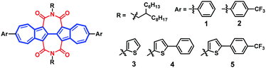 |
| | Fig. 3 Chemical structures of 6,6′-diaryl-substituted biazulene diimides 1–5. | |
Results and discussion
Synthesis and thermal stability
The synthetic routes of BAzDI derivatives 1–5 are shown in Scheme 1. Suzuki–Miyaura cross-coupling reactions of compound S176 with the corresponding arylboronic acids (phenylboronic acid, 4-(trifluoromethyl)phenylboronic acid and 2-thienylboronic acid) were carried out to give compounds S2a, S2b and S2c in 86%, 60% and 91% yields, respectively. It is clear that the coupling reactions are affected by the properties of the aryl group and the yields are increased by increasing the electron-donating abilities of the aryl groups. Chlorination of S2a–cvia Sandmeyer reaction using isoamyl nitrite and chlorotrimethylsilane in CHCl3 afforded dicarboxylates S3a, S3b and S3c with yields of ≥90%. Compounds S3a–c then efficiently underwent self-coupling reactions to afford tetracarboxylates S4a, S4b and S4c in 84–89% yields. Hydrolysis of S4a–c gave acids S5a, S5b and S5c in 82–89% yields, which were then treated with acetic anhydride, affording the intermediate dianhydrides S6a, S6b and S6c, with yields of 78–86%. Finally, compounds S6a–c were treated with 2-hexyldecylamine in refluxing dichloromethane, and after removing the dichloromethane, the residue then directly underwent an imidization reaction with sodium acetate and acetic anhydride to give BAzDI derivatives 1, 2 and 3 in 39%, 27% and 43% yields, respectively. After dibromination of 3 in the presence of Br2 in dichloromethane, precursor S7 was obtained in 92% yield, which then underwent Suzuki–Miyaura cross-coupling reactions with phenylboronic acid and 4-(trifluoromethyl)phenylboronic acid, affording BAzDI derivatives 4 and 5 in 71%, and 64% yields, respectively. Moreover, by using a similar synthetic procedure for 1 from S6a, the N,N′-dioctyl substituted BAzDI derivative 6 was synthesized in 50% yield. Compound 6 was used as the model to grow single crystals that are suitable for single crystal X-ray analysis to understand the molecular packing structure in the solid state.
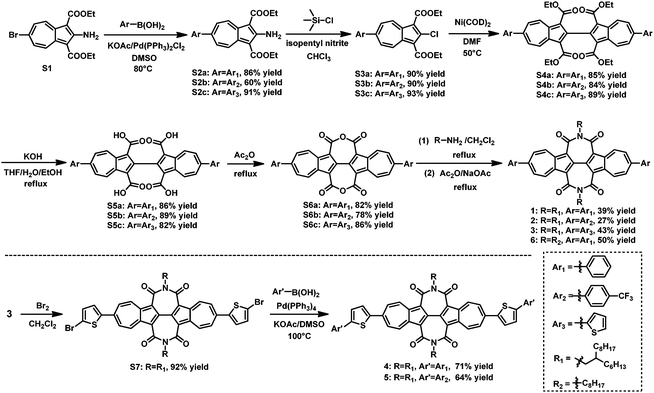 |
| | Scheme 1 Synthesis of aryl-substituted biazulene diimide derivatives (1–6). | |
The chemical structures of compounds 1–5 were fully characterized by 1H and 13C NMR spectra, mass spectrometry and IR spectroscopy as well as elemental analysis. At room temperature, compounds 1–5 are highly soluble in common organic solvents such as THF, CH2Cl2, CHCl3, and toluene, making them convenient to fabricate OFET and OPV devices by using solution-processable techniques. Thermogravimetric analysis (TGA) and differential scanning calorimetry (DSC) were performed under nitrogen atmosphere to investigate the thermal properties of compounds 1–5. All the compounds exhibit decomposition temperatures (with 5% weight loss) >380 °C, demonstrating their excellent thermal stability (Fig. S1, ESI†). As shown in Fig. S2 (ESI†), compounds 1–5 display obvious endothermic and exothermic peaks (186/176 °C, 200/183 °C, 231/221 °C, 227/218 °C and 270/266 °C for 1–5, respectively) in repeated heating–cooling DSC cycles, which could be assigned to the corresponding melting and crystallization processes.
X-ray crystallography
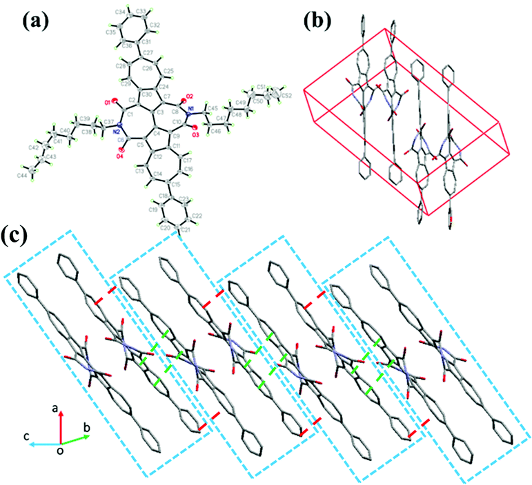
Single crystals of compound 6 were obtained by the slow diffusion of its chloroform and methanol solvents at room temperature. As illustrated in Fig. 4, the molecular skeleton of 6 is twisted with a dihedral angle of about 28.1° between two azulene rings, and dihedral angles between 2,2′-biazulene and the two respective imide rings are around 25.3°–28.3°. Besides, the dihedral angle between the azulene moiety and the adjacent phenyl ring is about 44°. However, as shown in Fig. 4a and b, compound 6 exhibits dense molecular packing in spite of its twisted molecular backbone. Two adjacent molecules of 6 in the crystal form a dimer through slightly slipped face to face π–π stacking with an interplanar distance of about 3.45 Å (Fig. 4) and short intermolecular atom–atom contacts (about 3.10–3.39 Å as shown in Fig. S3, ESI†). Between adjacent dimers, the electron-rich five-membered ring of one azulene moiety overlaps with the electron-poor seven-membered ring of the adjacent azulene unit due to the dipole moment of azulene, with an interplanar π–π stacking distance of about 3.39 Å, forming a slipped one-dimensional (1D) π–π stacking motif. This 1D molecular packing arrangement would favor charge carrier transport. Moreover, there are also interplanar π–π interactions between adjacent phenyl rings (∼3.5 Å, Fig. 4) and between phenyl rings and adjacent azulene units (∼3.4 Å) with short intermolecular atom–atom contacts of 3.10–3.37 Å. The single crystal analysis demonstrates that the 6,6′-diaryl-substituted BAzDI derivatives would be promising organic semiconductors due to efficient molecular packing in the solid state.
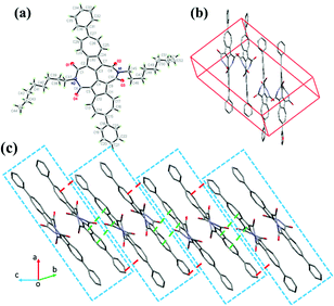 |
| | Fig. 4 Single-crystal structure of 6: (a) thermal ellipsoids diagram (probability level = 50%), (b) and (c) packing structure. | |
DFT calculations
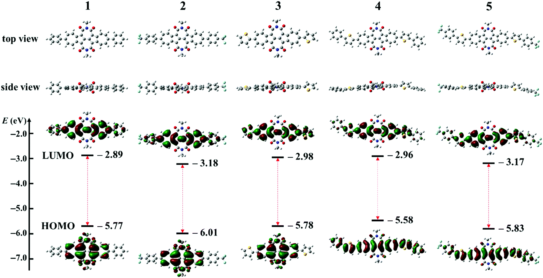
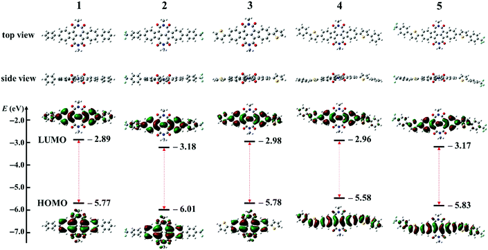
Density functional theory (DFT) calculations were carried out at the B3LYP/6-31G(d,p) level using the Gaussian 09 package with all alkyl chains replaced by methyl groups to reduce the time required. Fig. 5 shows the geometries and frontier molecular orbitals (FMO) with their energies of model molecules for BAzDI derivatives 1–5. All molecules exhibit a twisted molecular backbone, which is consistent with single crystal X-ray analysis. For all molecules, the electron density distribution of the LUMO is well spread over the azulene units and directly substituted aryl moieties. For the HOMO, there are no largest coefficients located on the phenyl or thienyl groups as well as the 2- and 6-positions of the azulene units of compounds 1–3. However, the electron density distribution of the HOMO is delocalized well through the whole molecule backbone of 4 and 5, since these two compounds have more extended π-systems. The results indicate that electron transport is more favored than hole transport for compounds 1–3 and compounds 4 and 5 are supposed to favor both electron and hole transport. As shown in Fig. 5, the FMO energies and HOMO–LUMO gaps of BAzDI derivatives 1–5 can be fine-tuned by adding different aryl groups at the 6- and 6′-positions, with HOMO levels ranging from −5.58 to −6.01 eV and LUMO values from −2.89 to −3.18 eV. Compounds 1–5 present narrower HOMO–LUMO gaps (2.62–2.88 eV) than the unsubstituted BAzDI (2.94 eV)31 induced by the extension of the π-conjugated system. Compounds 4 and 5 have narrower energy gaps (2.62 and 2.66 eV) than 3 (2.8 eV) due to the addition of two extra aryl groups. The FMO energies of 2 (HOMO/LUMO: −6.01/−3.18 eV) shift downward about 0.2–0.3 eV versus those of 1 (HOMO/LUMO: −5.77/−2.89 eV), as do the FMO energies of 5 (HOMO/LUMO: −5.83/−3.17 eV) versus those of 4 (HOMO/LUMO: −5.58/−2.96 eV). The downward-shift of FMO energies can be attributed to the electron-withdrawing ability of the two trifluoromethyl (TFM) groups, making compounds 2 and 5 more favorable for electron injection and transport. It is worthwhile to note that the suitable FMO energies along with the well-spread electron density distribution of both the HOMO and LUMO make 4 a possible ambipolar semiconductor.
 |
| | Fig. 5 The geometries, frontier molecular orbitals and their energies of model molecules for BAzDI derivatives 1–5 obtained by DFT calculations. | |
Optical and electrochemical properties
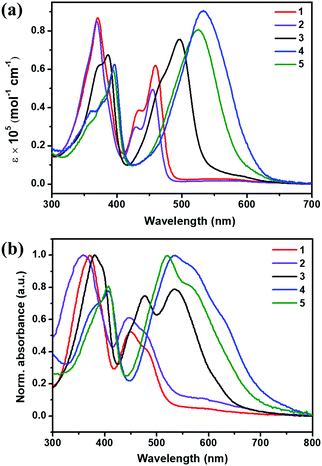
The optical and electrochemical properties of semiconductors 1–5 were investigated by UV-vis absorption spectra and cyclic voltammetry (CV) measurements. The optical and electrochemical data are listed in Table 1. Fig. 6 depicts the UV-vis absorption spectra of 1–5 in dichloromethane solution and in thin films. All the compounds display two main absorption bands in the range of 300–800 nm, where the former bands at 300–400 nm correspond to the π–π* transitions of the conjugated backbone, and the bands that appeared at lower energy can be ascribed to intramolecular charge transfer (ICT) transitions.77 Besides, compounds 1 and 2 exhibit a very weak absorption in the range of 500 to 650 nm, derived from the S0 → S1 transition of azulene.31 In contrast, compounds 3–5 with electron-donating thiophene units and more extended π-conjugated backbones show a broad and strong absorption from 400 to 650 nm, which can be assigned to the combination of ICT transitions and the S0 → S1 transitions of azulene. It is clear that the absorptions are influenced by the substituted aryl groups and the absorption maxima are hypsochromically shifted by decreasing the electron-donating abilities of the aryl groups. For instance, compared to the absorption of 3 at 496 nm in solution, those of 1 and 2 are blue shifted to 459 and 450 nm, respectively. As shown in Fig. 6b, in comparison with the corresponding absorptions in solution, the thin-film absorption spectra of these BAzDI derivatives are broadened and presented a red shift of about 21–40 nm for the end absorptions, as well as the newly formed shoulder peaks, indicating that strong molecular aggregation is presented within the thin films of compounds 1–5, which may facilitate charge carrier transport. The optical band gaps for compounds 1–5 are estimated from their onset absorptions in thin films and listed in Table 1. In spite of the difference in absorption spectral features, compounds 1, 2 and 3 have almost the same optical band gaps of about 1.68 eV, 1.69 eV and 1.68 eV, respectively. In comparison with 3, the absorption spectra of 4 and 5 show obvious red shifts, resulting in narrower optical band gaps of 1.59 eV and 1.61 eV, respectively. The changing trend of optical band gaps of 1–5 is consistent with that of their HOMO–LUMO gaps (2.88, 2.83, 2.80, 2.62 and 2.66 eV for compounds 1–5, respectively) estimated by DFT calculations.
Table 1 Optical, electrochemical and DFT calculation data for compounds 1–5
| Compound |
λ
max (nm) |
E
optg![[thin space (1/6-em)]](https://www.rsc.org/images/entities/char_2009.gif) a (eV) a (eV) |
E
red1onsetb (V) |
E
ox1onset
(V) |
LUMOc (eV) |
HOMOc (eV) |
E
CVg d (eV) |
LUMOe (eV) |
HOMOe (eV) |
E
Calge (eV) |
| Sol |
Film |
|
Estimated from the onset absorption of the thin film.
Onset potential versus SCE.
Calculated from EHOMO/LUMO = −4.44 − Eox1onset/Ered1onset (calibration by ferrocene).
Calculated from CV.
Estimated from DFT calculations.
|
|
1
|
371, 459 |
372, 451, 480 |
1.68 |
−0.81 |
1.47 |
−3.63 |
−5.91 |
2.28 |
−2.89 |
−5.77 |
2.88 |
|
2
|
369, 450 |
360, 447, 476 |
1.69 |
−0.71 |
1.60 |
−3.73 |
−6.04 |
2.31 |
−3.18 |
−6.01 |
2.85 |
|
3
|
386, 496 |
380, 477, 536 |
1.68 |
−0.81 |
1.46 |
−3.63 |
−5.90 |
2.27 |
−2.98 |
−5.78 |
2.8 |
|
4
|
396, 533 |
407, 536, 567 |
1.59 |
−0.80 |
1.24 |
−3.64 |
−5.68 |
2.04 |
−2.96 |
−5.58 |
2.62 |
|
5
|
394, 525 |
407, 521, 562 |
1.61 |
−0.72 |
1.34 |
−3.72 |
−5.78 |
2.06 |
−3.17 |
−5.83 |
2.66 |
 |
| | Fig. 6 UV-vis absorption spectra of compounds 1–5 in dichloromethane (a), and in thin films (b). | |
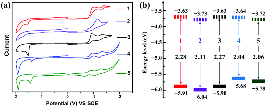
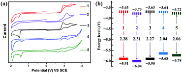
Fig. 7 shows the cyclic voltammograms and graphical representation of the experimental molecular energy levels of compounds 1–5. All the semiconductors exhibit irreversible or quasireversible reduction and irreversible oxidation processes in dichloromethane solution. As shown in Table 1, owing to the more electron-withdrawing ability of the 4-(trifluoromethyl)phenyl group relative to the phenyl unit, both the first onset reduction potential (Eonsetred1) and the first onset oxidation potential (Eonsetox1) of 2 (Eonsetred1/Eonsetox1 = −0.71/1.6 V) and 5 (Eonsetred1/Eonsetox1 = −0.72/1.34 V) are about 0.1 V anodically shifted compared with those of 1 (Eonsetred1/Eonsetox1 = −0.81/1.47 V) and 4 (Eonsetred1/Eonsetox1 = −0.80/1.24 V), respectively, indicating more electron affinity of 2 (or 5) versus1 (or 4). On the other hand, in comparison with compound 3 (Eonsetox1 = 1.46 V), compounds 4 (Eonsetox1 = 1.24 V) and 5 (Eonsetox1 = 1.34 V) with more extended π-conjugated skeletons present lower oxidation potentials, suggesting their possibility to transport hole carriers. The energy level of SCE was calibrated by ferrocene (energy level assumed to be −4.8 eV verses vacuum)78 and the half-wave potential of ferrocene/ferrocenium (Fc/Fc+) was found to be 0.36 V. The HOMO/LUMO energy levels were then calculated by using the equation: EHOMO/LUMO = −4.44 − Eox1onset/Ered1onset.79,80 The Eonsetred1 and Eonsetox1 of 1 are −0.81 V and 1.47 V, respectively. Accordingly, the EHOMO/LUMO value of 1 is estimated to be −5.91/−3.63 eV. Similarly, the EHOMO/LUMO values of 2–5 evaluated by CV measurements are −6.04/−3.73 eV, −5.90/−3.63 eV, −5.68/−3.64 eV and −5.78/−3.72 eV, respectively (Table 1), which are in agreement with the results by DFT calculations although there are deviations of about 0.6 eV. As shown in Fig. 7b, the energy levels of the BAzDI derivatives can be fine-tuned by altering the aryl groups connected at the 6- and 6′-positions. The experimental FMO energy levels combined with the DFT calculations of compounds 1–5 indicate that 1–3 are potential unipolar n-type semiconductors, while 4 and 5 may be ambipolar organic semiconductors.
 |
| | Fig. 7 (a) Cyclic voltammograms of compounds 1–5 in dichloromethane (0.1 M Bu4+NPF6− as supporting electrolyte; SCE as reference electrode; scan rate of 100 mV s−1). (b) Graphical representation of the experimental molecular energy levels of compounds 1–5. | |
OFET performance
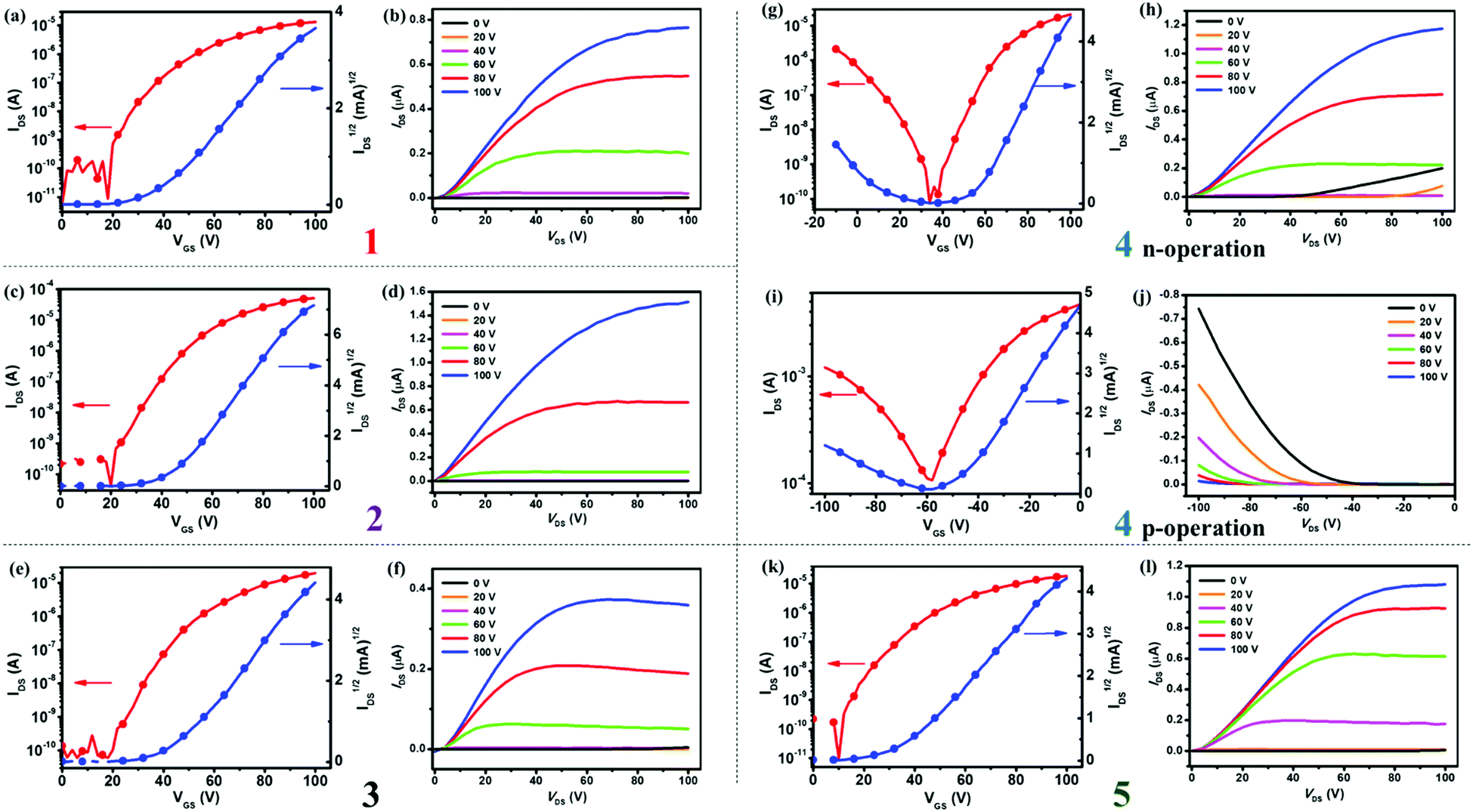
To investigate the charge transport properties of semiconductors 1–5, we fabricated their bottom-gate top-contact (BGTC) OFET devices by using spin-coating methods and measured them under nitrogen atmosphere with more than 15 devices for each compound (see ESI,† for details). Fig. 8 shows the typical transfer and output characteristics of OFETs based on 1–5, and the data are summarized in Table 2. As shown in Table 2, the as-spun thin film devices based on 1–5 exhibited relatively low electron mobilities (μe) of about 10−3–10−2 cm2 V−1 s−1. After thermal annealing at appropriate temperatures, thin films of 1–5 showed increased charge mobilities. For instance, with the annealing temperatures ranging from 80 to 120 °C, the electron mobilities of devices based on 1 and 3–5 manifested a stepwise improvement with μe of up to 0.15–0.37 cm2 V−1 s−1 and current on/off ratios (Ion/off) of 105–107 (see Table 2 for details). A similar trend holds true for ambipolar devices based on 4: the μe and μh values of the as-spun thin film devices were 6.8 × 10⁻² and 1 × 10⁻² cm2 V−1 s−1, respectively, when annealing at 120 °C, both μe and μh of thin films of 4 increased to 0.31 cm2 V−1 s−1 and 2.9 × 10⁻² cm2 V−1 s−1, respectively. When annealed at 80 °C, thin films of 2 presented an electron mobility of up to 0.52 cm2 V−1 s−1 with Ion/off of 106–107.
 |
| | Fig. 8 Transfer and output characteristics of BGTC OFETs based on semiconductors 1 (a and b), 2 (c and d), 3 (e and f), 4 (g and h for n-operation; (i and j) for p-operation) and 5 (k and l), respectively. | |
Table 2 Characteristics of OFETs based on 1–5 at different annealing temperatures (Ta)
| Compound |
T
a (°C) |
Polarity |
μ
e,max (μe,ave)a (cm2 V−1 s−1) |
V
T
(V) |
I
on
/I
off
|
μ
h,max (μh,ave)a (cm2 V−1 s−1) |
V
T
(V) |
I
on
/I
off
|
|
Measured under nitrogen atmosphere and calculated from at least 15 devices.
|
|
1
|
As-spun |
n |
2.9 × 10⁻² (2.3 × 10⁻²) |
44–53 |
104–105 |
— |
— |
— |
| 80 |
8.2 × 10⁻² (7.5 × 10⁻²) |
39–46 |
104–105 |
— |
— |
— |
| 120 |
0.15 (0.12) |
22–41 |
105–106 |
— |
— |
— |
|
|
|
2
|
As-spun |
n |
1.1 × 10⁻³ (8 × 10⁻⁴) |
39–45 |
103–104 |
— |
— |
— |
| 80 |
0.52 (0.45) |
27–35 |
106–107 |
— |
— |
— |
| 120 |
0.31 (0.25) |
10–23 |
106–107 |
— |
— |
— |
|
|
|
3
|
As-spun |
n |
5.7 × 10⁻³ (3.3 × 10⁻³) |
46–57 |
104–105 |
— |
— |
— |
| 80 |
8.1 × 10⁻² (7.2 × 10⁻²) |
34–47 |
104–105 |
— |
— |
— |
| 120 |
0.22 (0.16) |
24–36 |
105–106 |
— |
— |
— |
|
|
|
4
|
As-spun |
Ambipolar |
6.8 × 10⁻² (5.9 × 10⁻²) |
51–58 |
104–105 |
1 × 10⁻² (6.3 × 10⁻³) |
−(58–68) |
102–104 |
| 80 |
0.14 (0.11) |
40–49 |
105–106 |
1.2 × 10⁻² (9.8 × 10⁻³) |
−(55–66) |
102–104 |
| 120 |
0.31 (0.24) |
33–43 |
105–106 |
2.9 × 10⁻² (2.3 × 10⁻²) |
−(57–64) |
10–103 |
|
|
|
5
|
As-spun |
n |
3.4 × 10⁻² (2.8 × 10⁻²) |
33–49 |
105–106 |
— |
— |
— |
| 80 |
0.23 (0.18) |
28–43 |
105–106 |
— |
— |
— |
| 120 |
0.37 (0.31) |
21–35 |
106–107 |
— |
— |
— |
The results demonstrate that thin films of 1–3 and 5 display unipolar n-type semiconducting properties, whereas the thin film of 4 exhibits ambipolar charge transport behavior. The different semiconducting properties of these materials are related to their FMO energies, that is, all materials have relatively low LUMO energies (−3.63 to −3.73 eV) for electron transport, whereas the semiconductor 4 has a higher HOMO energy (−5.68 eV) than the others (−5.78 to −6.04 eV), making it suitable for hole injection and transport (see Table 1). Moreover, compounds 2 and 4 with lower LUMO energy levels (about −3.7 eV) derived from the electron-withdrawing TFM groups exhibited higher electron mobilities (0.37–0.52 cm2 V−1 s−1) than the others. On the whole, all semiconductors exhibited high device performance with average electron mobilities of 0.12–0.45 cm2 V−1 s−1. As revealed by single crystal analysis, the excellent electron transport performance of compounds 1–5 might be ascribed to the dense molecular packing induced by the dipolar moment of the azulene units. Besides, OFETs based on 2 displayed the best device performance with an average electron mobility of 0.45 cm2 V−1 s−1, and a maximum mobility of 0.52 cm2 V−1 s−1 obtained from low-temperature-annealed (80 °C) thin films, which is the highest electron mobility for azulene-based OSCs reported to date. There are few solution-processable n-type OSCs with mobilities ≥0.5 cm2 V−1 s−1,18 and thus, compound 2 is among the best unipolar n-type semiconductors for solution-processed OFETs. The results demonstrate that BAzDI derivatives with aryl groups substituted at the 6- and 6′-positions could not only fine-tune the FMO energy levels, resulting in different charge transport behaviors, but also display high electron mobilities (0.15–0.52 cm2 V−1 s−1).
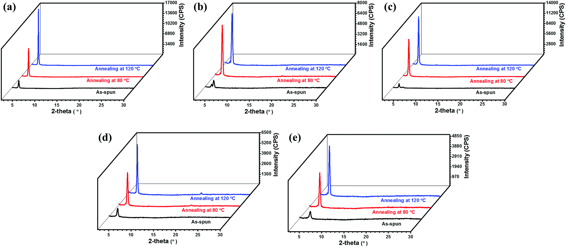
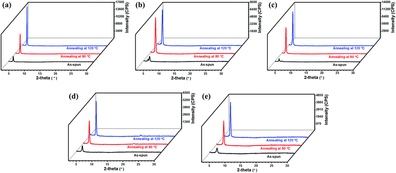
X-ray diffraction (XRD) and atomic force microscopy (AFM) were utilized to investigate the microstructures and surface topographic features of the as-spun and thermally annealed thin films of 1–5. Fig. 9 shows the XRD patterns of thin films of 1–5 before and after thermal annealing. It can be seen that only weak diffraction peaks were observed for the as-spun thin films of all the semiconductors, indicating a low crystallinity. After thermal annealing, all of the thin films exhibited stronger and sharper Bragg reflections, indicating a higher degree of crystallinity. Besides, the diffraction patterns of thin films of semiconductors 1–5 are correlated well with the changes of the device performance upon thermal annealing. For instance, the intensities of the diffraction peaks of thin films of 1 and 3–5 were enhanced stepwise after thermal annealing at 80 and 120 °C, corresponding well to the stepwise increased electron mobility. The d spacings of the as-spun thin films of compounds 1 and 3–5 are 20.8 Å, 21.6 Å, 18.4 Å and 16.9 Å, respectively, and remained almost unchanged after thermal annealing. On the other hand, thermal annealing treatments of thin films cause different changes in diffraction patterns for compound 2 (see Fig. 9 for detail). The diffraction peaks of thin films of 2 were found to become stronger and sharper upon thermal annealing at 80 °C. Then they remained almost unchanged when further annealed at 120 °C. These are consistent with the results that thin films of compound 2 exhibited the highest mobility when annealed at 80 °C. Interestingly, it is noted that the as-spun thin film of 2 displayed two closely neighboring peaks with 2θ of 4.33° and 4.80°, corresponding to d spacings of 20.4 and 18.4 Å, respectively, suggesting the coexistence of two phases/orientations in the as-spun thin films. After thermal annealing, both peaks disappeared, and a new strong diffraction peak with 2θ = 4.53° (corresponding to d spacing of 19.5 Å) was detected, indicating that the phases/orientations in the annealed films become uniform, which is well in accordance with the rapidly increased device performance upon thermal annealing.
 |
| | Fig. 9 X-ray diffraction patterns of thin films of semiconductors 1 (a), 2 (b), 3 (c), 4 (d) and 5 (e). | |
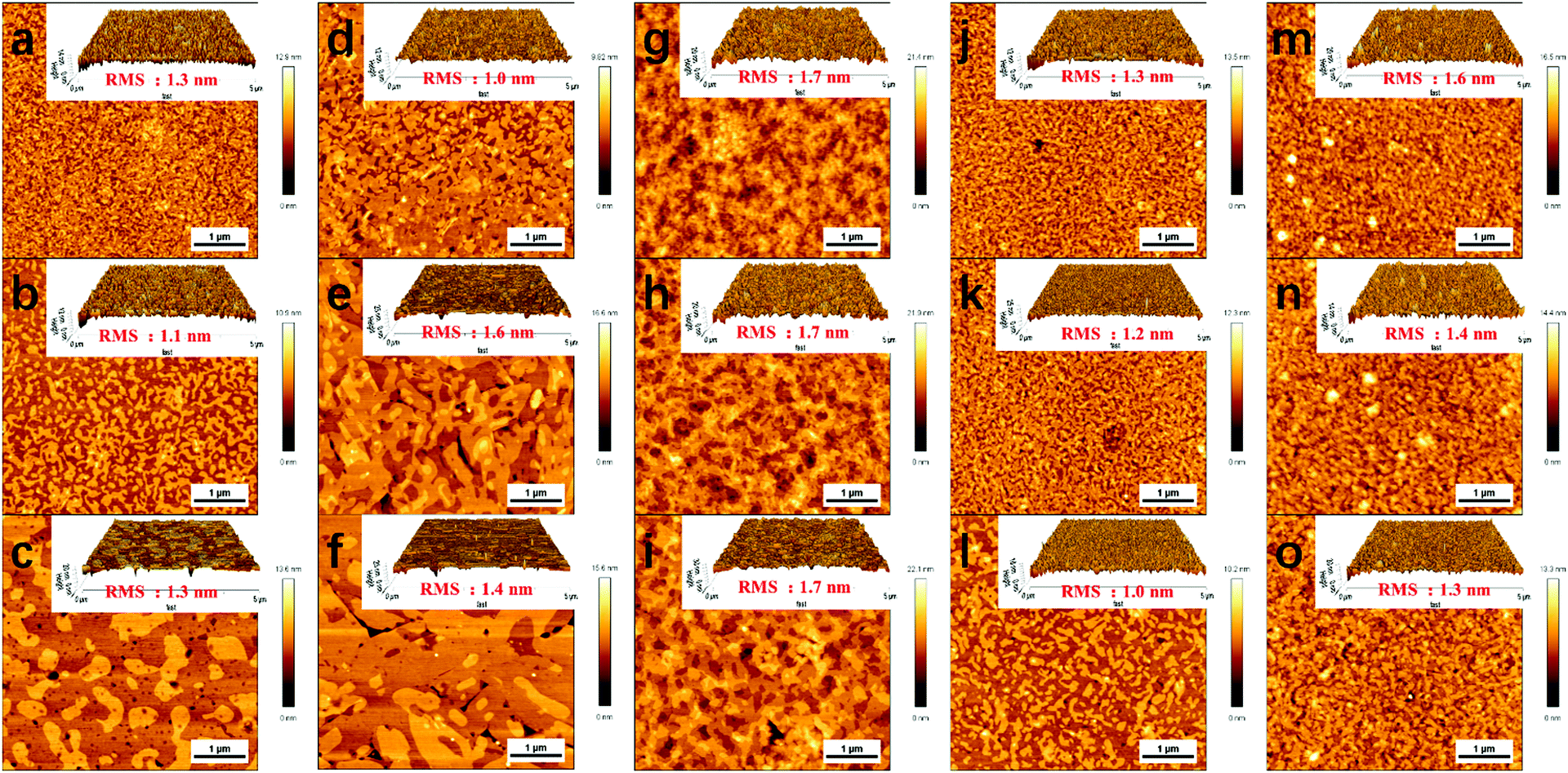
Fig. 10 depicts the AFM images of the as-spun and annealed thin films of 1–5. After thermal annealing, visible changes in thin film morphology were observed for each semiconductor. Besides the smooth, uniform, and crystalline film morphology features with small root mean square (RMS) roughness of about 1–2 nm, all the compounds presented similar film morphology variations upon thermal annealing, that is, the grain size increased accompanied by the grain boundaries decreasing. The improved film morphology and crystallinity upon thermal annealing agree well with the improved device performance (Table 2).
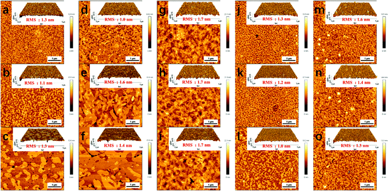 |
| | Fig. 10 AFM images of the as-spun (a, d, g, j and m) and annealed (b, e, h, k and n, annealed at 80 °C; c, f, i, l and o, annealed at 120 °C) thin films of semiconductors 1 (a–c), 2 (d–f), 3 (g–i), 4 (j–l) and 5 (m–o). Insets are respective 3D images disclosing the roughness of the thin films. | |
Photovoltaic performance
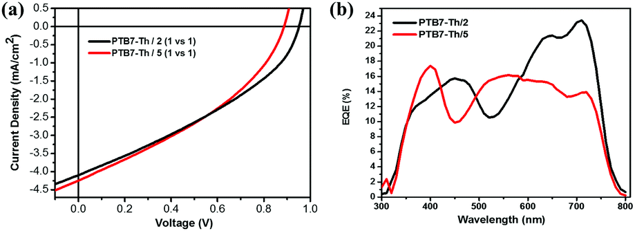
Judging from their suitable HOMO/LUMO energy levels and high electron mobilities, compounds 2 and 5 are considered to be potential electron acceptors for photovoltaic materials, and we fabricated OPV devices with these two molecules as electron acceptors and widely used PTB7-Th (ESI,† inset of Fig. S4) as an electron donor. An inverted device structure of ITO/ZnO/active layer/MoO3/Ag was used. Fig. 11a and b show the current density–voltage (J–V) curves and external quantum efficiency (EQE) spectra of devices based on the PTB7-Th:2 and PTB7-Th:5 blends, respectively. The photovoltaic parameters and charge mobilities of blend films measured by the space-charge-limited current (SCLC) method are summarized in Table 3. SCLC fittings of the hole-only devices and electron-only devices are shown in Fig. S5 and S6 (ESI†), respectively. OPV devices with the PTB7-Th:2 blend as the active layer exhibit a maximum PCE value of 1.38% with an open-circuit voltage (Voc) of 0.95 V, a short-circuit density (Jsc) of 4.09 mA cm−2, and a fill factor (FF) of 35.49%. Similarly, OPV devices with the PTB7-Th:5 blend as the active layer provide a PCE value of 1.36% with an Voc value of 0.88 V, a Jsc value of 4.24 mA cm−2, and a FF value of 36.35%. To the best of our knowledge, most of the electron acceptors for OPVs, including fullerene and non-fullerene acceptors, are generally constructed by benzene, thiophene and other traditional aromatic rings, and electron acceptors based on non-traditional aromatic units such as azulene are rarely reported.8,9,81 The results demonstrate that these two azulene-based molecules are promising electron acceptors for OPVs with high Voc values. The unsatisfactory device performance may be ascribed to the relatively low short-circuit density (Jsc), caused by unbalanced charge mobilities and low fill factor (FF) as well as poor EQE (Fig. 11b). XRD patterns and AFM images of the blend films of PTB7-Th:2 and PTB7-Th:5 are shown in Fig. S4 and S7 (ESI†), respectively. The crude and featureless film morphology is unfavourable for exciton diffusion and charge transport, and might partly explain the relatively low PCE values.
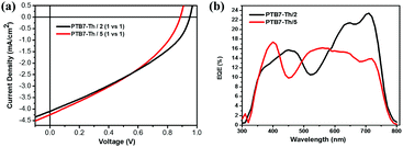 |
| | Fig. 11
J–V curves (a) and EQE spectra (b) of the photovoltaic devices based on the PTB7-Th:2 and PTB7-Th:5 blends, respectively. | |
Table 3 Summary of the performance of OPV devices
| Active layer |
V
OC (V) |
J
SC (mA cm−2) |
FF (%) |
PCEmax (PCEave)a (%) |
μ
h
(cm2 V−1 s−1) |
μ
e
(cm2 V−1 s−1) |
|
The average PCE value is calculated from 12 devices.
Measured by the space-charge-limited current (SCLC) method.
|
| PTB7-Th:2 |
0.95 |
4.09 |
35.49 |
1.38 (1.30) |
2.3 × 10⁻⁵ |
2.7 × 10⁻⁶ |
| PTB7-Th:5 |
0.88 |
4.24 |
36.35 |
1.36 (1.29) |
1.2 × 10⁻⁴ |
5.1 × 10⁻⁶ |
Conclusions
In this contribution, we presented five biazulene diimide (BAzDI) derivatives 1–5 with different aryl groups substituted at the 6- and 6′-positions. The syntheses, optical and electrochemical properties as well as semiconducting behaviors were investigated. By incorporating various aryl groups in the 6- and 6′-positions of BAzDI, the optoelectronic properties and energy levels of these compounds were successfully modulated. Compounds 1–3 and 5 are typical n-type organic semiconductors, and their solution-processed bottom-gate-top-contact OFET devices exhibited high device performance, with maximum electron mobilities of 0.15–0.52 cm2 V−1 s−1, and current on/off ratios >105. In comparison with compounds 1–3 and 5, semiconductor 4 with a higher HOMO energy level (−5.68 eV) and a narrower energy gap (2.04 eV from CV) displayed ambipolar charge transport behavior with an electron mobility of 0.31 cm2 V−1 s−1 and a hole mobility of 0.029 cm2 V−1 s−1. Single crystal analysis of 6 (a model molecule of 1) demonstrates that the dense molecular π–π stacking induced by the dipolar moment of azulene moieties might partly explain the excellent electron transport performance of these 6,6′-diaryl-substituted BAzDI derivatives. In addition, organic photovoltaic devices with PTB7-Th as the electron donor and compounds 2 and 5 as the electron acceptor exhibited power conversion efficiencies (PCEs) of 1.38% and 1.36%, respectively. All of these results demonstrate that 6,6′-diaryl-substituted BAzDIs are promising organic optoelectronic materials and azulene, a non-traditional aromatic hydrocarbon with large dipole moment, could be cleverly utilized to construct high performance OSCs. Further investigations on the design and synthesis of novel azulene-based OSCs with excellent semiconducting performance and new functions are currently underway in our laboratory.
Conflicts of interest
There are no conflicts to declare.
Acknowledgements
This research was financially supported by the National Natural Science Foundation (21522209 and 21502218), the “Strategic Priority Research Program” (XDB12010100), the Shanghai Science and Technology Committee (16JC1400603), and SIOC. We thank the Instrumental Analysis Center of Shanghai Jiao Tong University for X-ray crystallographic analysis.
References
- A. G. Anderson and B. M. Steckler, J. Am. Chem. Soc., 1959, 81, 4941–4946 CrossRef CAS.
- S. Jamali, N. A. Mousavi, M. Bagherzadeh, R. Kia and H. Samouei, Dalton Trans., 2017, 46, 11327–11334 RSC.
- T. Shoji, S. Sugiyama, T. Araki, A. Ohta, R. Sekiguchi, S. Ito, S. Mori, T. Okujima and M. Yasunami, Org. Biomol. Chem., 2017, 15, 3917–3923 CAS.
- Y. Zhou, Y. Zhuang, X. Li, H. Agren, L. Yu, J. Ding and L. Zhu, Chem. – Eur. J., 2017, 23, 7642–7647 CrossRef CAS PubMed.
- T. Shoji, D. Nagai, M. Tanaka, T. Araki, A. Ohta, R. Sekiguchi, S. Ito, S. Mori and T. Okujima, Chem. – Eur. J., 2017, 23, 5126–5136 CrossRef CAS PubMed.
- T. Shoji and S. Ito, Chem. – Eur. J., 2017, 23, 16696–16709 CrossRef CAS PubMed.
- J. Michl and E. W. Thulstrup, Tetrahedron, 1976, 32, 205–209 CrossRef CAS.
- J.-X. Dong and H.-L. Zhang, Chin. Chem. Lett., 2016, 27, 1097–1104 CrossRef CAS.
- H. Xin and X. Gao, ChemPlusChem, 2017, 82, 945–956 CrossRef CAS.
- X. Shi, A. Sasmal, J.-F. Soulé and H. Doucet, Chem. – Asian J., 2018, 13, 143–157 CrossRef CAS PubMed.
- F. Wang, Y.-H. Lai and M.-Y. Han, Macromolecules, 2004, 37, 3222–3230 CrossRef CAS.
- P. G. Lacroix, I. Malfant, G. Iftime, A. C. Razus, K. Nakatani and J. A. Delaire, Chem. – Eur. J., 2000, 6, 2599–2608 CrossRef CAS.
- L. Cristian, I. Sasaki, P. G. Lacroix, B. Donnadieu, I. Asselberghs, K. Clays and A. C. Razus, Chem. Mater., 2004, 16, 3543–3551 CrossRef CAS.
- A. Migalska-Zalas, Y. El kouari and S. Touhtouh, Opt. Mater., 2012, 34, 1639–1643 CrossRef CAS.
- J. T. E. Quinn, J. Zhu, X. Li, J. Wang and Y. Li, J. Mater. Chem. C, 2017, 5, 8654–8681 RSC.
- X. Wang, J. K.-P. Ng, P. Jia, T. Lin, C. M. Cho, J. Xu, X. Lu and C. He, Macromolecules, 2009, 42, 5534–5544 CrossRef CAS.
- E. Amir, R. J. Amir, L. M. Campos and C. J. Hawker, J. Am. Chem. Soc., 2011, 133, 10046–10049 CrossRef CAS PubMed.
- K. Tsurui, M. Murai, S.-Y. Ku, C. J. Hawker and M. J. Robb, Adv. Funct. Mater., 2014, 24, 7338–7347 CrossRef CAS.
- E. H. Ghazvini Zadeh, A. W. Woodward, D. Richardson, M. V. Bondar and K. D. Belfield, Eur. J. Org. Chem., 2015, 2271–2276 CrossRef CAS.
-
(a) F. Schwarz, M. Koch, G. Kastlunger, H. Berke, R. Stadler, K. Venkatesan and E. Lörtscher, Angew. Chem., Int. Ed., 2016, 55, 11781–11786 CrossRef CAS PubMed;
(b) G. Yang, S. Sangtarash, Z. Liu, X. Li, H. Sadeghi, Z. Tan, R. Li, J. Zheng, X. Dong, J. Liu, Y. Yang, J. Shi, Z. Xiao, G. Zhang, C. Lambert, W. Hong and D. Zhang, Chem. Sci., 2017, 8, 7505–7509 RSC.
- T. Shoji, E. Shimomura, M. Maruyama, A. Maruyama, S. Ito, T. Okujima, K. Toyota and N. Morita, Eur. J. Org. Chem., 2013, 7785–7799 CrossRef CAS.
- H. Salman, Y. Abraham, S. Tal, S. Meltzman, M. Kapon, N. Tessler, S. Speiser and Y. Eichen, Eur. J. Org. Chem., 2005, 2207–2212 CrossRef CAS.
- K. Kurotobi, K. S. Kim, S. B. Noh, D. Kim and A. Osuka, Angew. Chem., Int. Ed., 2006, 45, 3944–3947 CrossRef CAS PubMed.
- F. Wang, T. T. Lin, C. He, H. Chi, T. Tang and Y.-H. Lai, J. Mater. Chem., 2012, 22, 10448 RSC.
- E. C. P. Smits, S. Setayesh, T. D. Anthopoulos, M. Buechel, W. Nijssen, R. Coehoorn, P. W. M. Blom, B. deBoer and D. M. deLeeuw, Adv. Mater., 2007, 19, 734–738 CrossRef CAS.
- P. H. Wobkenberg, J. G. Labram, J.-M. Swiecicki, K. Parkhomenko, D. Sredojevic, J.-P. Gisselbrecht, D. M. de Leeuw, D. D. C. Bradley, J.-P. Djukic and T. D. Anthopoulos, J. Mater. Chem., 2010, 20, 3673–3680 RSC.
- Y. Yamaguchi, Y. Maruya, H. Katagiri, K.-I. Nakayama and Y. Ohba, Org. Lett., 2012, 14, 2316–2319 CrossRef CAS PubMed.
- Y. Yamaguchi, K. Ogawa, K.-I. Nakayama, Y. Ohba and H. Katagiri, J. Am. Chem. Soc., 2013, 135, 19095–19098 CrossRef CAS PubMed.
- Y. Yamaguchi, M. Takubo, K. Ogawa, K.-I. Nakayama, T. Koganezawa and H. Katagiri, J. Am. Chem. Soc., 2016, 138, 11335–11343 CrossRef CAS PubMed.
- J. Yao, Z. Cai, Z. Liu, C. Yu, H. Luo, Y. Yang, S. Yang, G. Zhang and D. Zhang, Macromolecules, 2015, 48, 2039–2047 CrossRef CAS.
- H. Xin, C. Ge, X. Yang, H. Gao, X. Yang and X. Gao, Chem. Sci., 2016, 7, 6701–6705 RSC.
- H. Xin, C. Ge, L. Fu, X. Yang and X. Gao, Chin. J. Org. Chem., 2017, 37, 711–719 CrossRef CAS.
- H. Xin, C. Ge, X. Jiao, X. Yang, K. Rundel, C. R. McNeill and X. Gao, Angew. Chem., 2018, 130, 1336–1340 CrossRef.
- E. Puodziukynaite, H.-W. Wang, J. Lawrence, A. J. Wise, T. P. Russell, M. D. Barnes and T. Emrick, J. Am. Chem. Soc., 2014, 136, 11043–11049 CrossRef CAS PubMed.
- H. Nishimura, N. Ishida, A. Shimazaki, A. Wakamiya, A. Saeki, L. T. Scott and Y. Murata, J. Am. Chem. Soc., 2015, 137, 15656–15659 CrossRef CAS PubMed.
- A. R. Murphy and J. M. J. Fréchet, Chem. Rev., 2007, 107, 1066–1096 CrossRef CAS PubMed.
- X. Guo, A. Facchetti and T. J. Marks, Chem. Rev., 2014, 114, 8943–9021 CrossRef CAS PubMed.
- C. Wang, H. Dong, W. Hu, Y. Liu and D. Zhu, Chem. Rev., 2012, 112, 2208–2267 CrossRef CAS PubMed.
- Y. Lin, H. Fan, Y. Li and X. Zhan, Adv. Mater., 2012, 24, 3087–3106 CrossRef CAS PubMed.
- Y. Zhao, Y. Guo and Y. Liu, Adv. Mater., 2013, 25, 5372–5391 CrossRef CAS PubMed.
- M. Gsänger, D. Bialas, L. Huang, M. Stolte and F. Würthner, Adv. Mater., 2016, 28, 3615–3645 CrossRef PubMed.
- C. Li, M. Liu, N. G. Pschirer, M. Baumgarten and K. Müllen, Chem. Rev., 2010, 110, 6817–6855 CrossRef CAS PubMed.
- S. Holliday, J. E. Donaghey and I. McCulloch, Chem. Mater., 2014, 26, 647–663 CrossRef CAS.
- T. Lei, J.-Y. Wang and J. Pei, Acc. Chem. Res., 2014, 47, 1117–1126 CrossRef CAS PubMed.
- L. Shi, Y. Guo, W. Hu and Y. Liu, Mater. Chem. Front., 2017, 1, 2423–2456 RSC.
- N. Liang, W. Jiang, J. Hou and Z. Wang, Mater. Chem. Front., 2017, 1, 1291–1303 RSC.
- Z. Hu, L. Ying, F. Huang and Y. Cao, Sci. China: Chem., 2017, 60, 571–582 CrossRef CAS.
- J. Ma, Z. Liu, Z. Wang, Y. Yang, G. Zhang, X. Zhang and D. Zhang, Mater. Chem. Front., 2017, 1, 2547–2553 RSC.
- C. Zhang, T. Liu, W. Zeng, D. Xie, Z. Luo, Y. Sun and C. Yang, Mater. Chem. Front., 2017, 1, 749–756 RSC.
- G. E. Rudebusch, J. L. Zafra, K. Jorner, K. Fukuda, J. L. Marshall, I. Arrechea-Marcos, G. L. Espejo, R. Ponce Ortiz, C. J. Gómez-García, L. N. Zakharov, M. Nakano, H. Ottosson, J. Casado and M. M. Haley, Nat. Chem., 2016, 8, 753 CrossRef CAS PubMed.
- J. Zhang, P. Gu, G. Long, R. Ganguly, Y. Li, N. Aratani, H. Yamada and Q. Zhang, Chem. Sci., 2016, 7, 3851–3856 RSC.
- M. J. Ford, M. Wang, S. N. Patel, H. Phan, R. A. Segalman, T.-Q. Nguyen and G. C. Bazan, Chem. Mater., 2016, 28, 1256–1260 CrossRef CAS.
- J. L. Marshall, K. Uchida, C. K. Frederickson, C. Schutt, A. M. Zeidell, K. P. Goetz, T. W. Finn, K. Jarolimek, L. N. Zakharov, C. Risko, R. Herges, O. D. Jurchescu and M. M. Haley, Chem. Sci., 2016, 7, 5547–5558 RSC.
- X. Zhao, C. Ge, X. Yang and X. Gao, Mater. Chem. Front., 2017, 1, 1635–1640 RSC.
- P.-Y. Gu, Z. Wang, G. Liu, H. Yao, Z. Wang, Y. Li, J. Zhu, S. Li and Q. Zhang, Chem. Mater., 2017, 29, 4172–4175 CrossRef CAS.
- R. Sandoval-Torrientes, J. Calbo, W. Matsuda, W. Choi, J. Santos, S. Seki, E. Ortí and N. Martín, ChemPlusChem, 2017, 82, 1105–1111 CrossRef CAS.
- M. A. McCarthy, B. Liu, E. P. Donoghue, I. Kravchenko, D. Y. Kim, F. So and A. G. Rinzler, Science, 2011, 332, 570–573 CrossRef CAS PubMed.
- J. Li, Y. Zhao, H. S. Tan, Y. Guo, C.-A. Di, G. Yu, Y. Liu, M. Lin, S. H. Lim, Y. Zhou, H. Su and B. S. Ong, Sci. Rep., 2012, 2, 754 CrossRef PubMed.
- I. Kang, H.-J. Yun, D. S. Chung, S.-K. Kwon and Y.-H. Kim, J. Am. Chem. Soc., 2013, 135, 14896–14899 CrossRef CAS PubMed.
- G. Kim, S.-J. Kang, G. K. Dutta, Y.-K. Han, T. J. Shin, Y.-Y. Noh and C. Yang, J. Am. Chem. Soc., 2014, 136, 9477–9483 CrossRef CAS PubMed.
- K. Nakayama, Y. Hirose, J. Soeda, M. Yoshizumi, T. Uemura, M. Uno, W. Li, M. J. Kang, M. Yamagishi, Y. Okada, E. Miyazaki, Y. Nakazawa, A. Nakao, K. Takimiya and J. Takeya, Adv. Mater., 2011, 23, 1626–1629 CrossRef CAS PubMed.
- Y. Yuan, G. Giri, A. L. Ayzner, A. P. Zoombelt, S. C. B. Mannsfeld, J. Chen, D. Nordlund, M. F. Toney, J. Huang and Z. Bao, Nat. Commun., 2014, 5, 3005 Search PubMed.
- C. Luo, A. K. K. Kyaw, L. A. Perez, S. Patel, M. Wang, B. Grimm, G. C. Bazan, E. J. Kramer and A. J. Heeger, Nano Lett., 2014, 14, 2764–2771 CrossRef CAS PubMed.
- X. Gao and Y. Hu, J. Mater. Chem. C, 2014, 2, 3099–3117 RSC.
- X. Gao and Z. Zhao, Sci. China: Chem., 2015, 58, 947–968 CrossRef CAS.
- J. T. E. Quinn, J. Zhu, X. Li, J. Wang and Y. Li, J. Mater. Chem. C, 2017, 5, 8654–8681 RSC.
- Q. Wu, R. Li, W. Hong, H. Li, X. Gao and D. Zhu, Chem. Mater., 2011, 23, 3138–3140 CrossRef CAS.
- F. Zhang, Y. Hu, T. Schuettfort, C. A. Di, X. Gao, C. R. McNeill, L. Thomsen, S. C. Mannsfeld, W. Yuan, H. Sirringhaus and D. Zhu, J. Am. Chem. Soc., 2013, 135, 2338–2349 CrossRef CAS PubMed.
- J. Li, X. Qiao, Y. Xiong, H. Li and D. Zhu, Chem. Mater., 2014, 26, 5782–5788 CrossRef CAS.
- C. Zhang, Y. Zang, E. Gann, C. R. McNeill, X. Zhu, C.-A. Di and D. Zhu, J. Am. Chem. Soc., 2014, 136, 16176–16184 CrossRef CAS PubMed.
- B. Crone, A. Dodabalapur, Y. Y. Lin, R. W. Filas, Z. Bao, A. LaDuca, R. Sarpeshkar, H. E. Katz and W. Li, Nature, 2000, 403, 521 CrossRef CAS PubMed.
- H. Klauk, U. Zschieschang, J. Pflaum and M. Halik, Nature, 2007, 445, 745 CrossRef CAS PubMed.
- E. J. Meijer, D. M. de Leeuw, S. Setayesh, E. van Veenendaal, B. H. Huisman, P. W. M. Blom, J. C. Hummelen, U. Scherf and T. M. Klapwijk, Nat. Mater., 2003, 2, 678 CrossRef CAS PubMed.
- R. Schmidt, M. M. Ling, J. H. Oh, M. Winkler, M. Könemann, Z. Bao and F. Würthner, Adv. Mater., 2007, 19, 3692–3695 CrossRef CAS.
- J. Mei, Y. Diao, A. L. Appleton, L. Fang and Z. Bao, J. Am. Chem. Soc., 2013, 135, 6724–6746 CrossRef CAS PubMed.
- R. N. McDonald, J. M. Richmond, J. R. Curtis, H. E. Petty and T. L. Hoskins, J. Org. Chem., 1976, 41, 1811–1821 CrossRef CAS.
- B. Fu, J. Baltazar, Z. Hu, A.-T. Chien, S. Kumar, C. L. Henderson, D. M. Collard and E. Reichmanis, Chem. Mater., 2012, 24, 4123–4133 CrossRef CAS.
- D. M. de Leeuw, M. M. J. Simenon, A. R. Brown and R. E. F. Einerhand, Synth. Met., 1997, 87, 53–59 CrossRef CAS.
- Y. Liu, M. S. Liu and A. K. Y. Jen, Acta Polym., 1999, 50, 105–108 CrossRef CAS.
- H. Usta, A. Facchetti and T. J. Marks, J. Am. Chem. Soc., 2008, 130, 8580–8581 CrossRef CAS PubMed.
- C. Dou, J. Liu and L. Wang, Sci. China: Chem., 2017, 60, 450–459 CrossRef CAS.
Footnote |
| † Electronic supplementary information (ESI) available: Materials and general methods, synthesis and characterizations, TGA and DSC curves, OFET and photovoltaic device fabrication and measurement, NMR spectra, mass spectra and X-ray crystallographic data. CCDC 1819497. For ESI and crystallographic data in CIF or other electronic format see DOI: 10.1039/c8qm00047f |
|
| This journal is © the Partner Organisations 2018 |
Click here to see how this site uses Cookies. View our privacy policy here. 
 *a
*a