DOI:
10.1039/C7QM00620A
(Research Article)
Mater. Chem. Front., 2018,
2, 475-482
Kirigami nanofluidics†
Received
29th December 2017
, Accepted 19th January 2018
First published on 19th January 2018
Abstract
Exfoliated thin sheets of layered materials can readily reassemble to form a macroscopic lamellar film containing a massive array of parallel two-dimensional (2D) nanochannels. These 2D nanofluidic channels exhibit enhanced unipolar ionic conductivity with the counterions as the majority charge carriers, thus conceptually become an ionic analogue of extrinsically doped semiconductor wafers. Here we demonstrate “kirigami nanofluidics”, where ionic transport can be manipulated by tailor-cutting the shape of the film. Shapes with an asymmetric source and drain exhibit rectifying ionic currents, which is attributed to the asymmetric concentration polarization zones developed in the two reservoirs. Therefore, the rectification ratio can be continuously tuned simply by adjusting the relative edge sizes of the shape, or even programmed by selecting the number of source and drain branches in multi-armed shapes. Kirigami-made ionic rectifiers and resistors can be conveniently connected together to demonstrate simple AND and OR logic functions. These results demonstrate nanoscale ionic transport can be manipulated by patterning materials at the macroscopic length scale.
Introduction
An electrolyte confined in nanochannels exhibits unusual behaviors owing to strong influences from the channel walls. When the size of a charged channel is comparable to the Debye length of the electrolyte, co-ions are effectively repelled from the channel and counterions are concentrated, leading to unipolar ionic transport properties with the counterions as the majority charge carriers.1–5 This is conceptually analogous to extrinsically doped semiconductors, a material foundation that has enabled the realization of numerous electronic devices and integrated circuits.6 Nanofluidic systems have been extensively employed to demonstrate similar devices using ions as charge carriers.7–13 Diodes, the most basic type of semiconductor device, have been an appealing model system for nanofluidic studies. Since ion transport through the nanochannels is strongly regulated by the interplay between surface charge, Debye length, and channel dimensions, diode-like ionic current rectification can be achieved by breaking the symmetry of these parameters at the two terminals of the nanochannels.14–18 For example, symmetric nanochannels may exhibit asymmetric transport characteristics if the electrolyte concentrations at the source and drain reservoirs are different.19 A more common strategy is to fabricate nanochannels with asymmetric sizes and inner surface properties, which typically relies on extensive use of lithography and has been hard to scale up.7,8,18
Recently, reconstructed layered membranes have been adopted by several research groups as a promising material platform for nanofluidics.20–26 Such membranes are readily made by restacking exfoliated thin sheets such as graphene oxide (GO) or clay, and contain a high volume fraction of interconnected 2D nanochannels (Fig. 1a). Here, nanochannel fabrication is straightforward and scalable, and does not rely on lithography or etching. Compared to other scalable nanofluidic materials such as anodized aluminum oxide membranes,27 block copolymer membranes28 and nanofluidic crystals,29,30 a unique feature of these layered membranes is that the channels are horizontally aligned and the channel height (i.e., interlayer spacing), which is responsible for confinement of the electrolyte, remains uniform throughout the entire thin film. Therefore, nanofluidic ionic transport properties are maintained regardless of the lateral dimensions or shape of the 2D nanochannel network. This opens up a range of new opportunities for manipulating ionic transport by tailoring the shape of the films (Fig. 1c), a process that we term “kirigami nanofluidics”. Here, we report new findings regarding rectifying 2D nanofluidic films and a new mechanism. Based on these new insights, we demonstrate several types of ionic diodes, whose rectification ratios are tunable via the geometries of the final cut. Proof-of-concept logic circuits are also assembled from kirigami made elements.
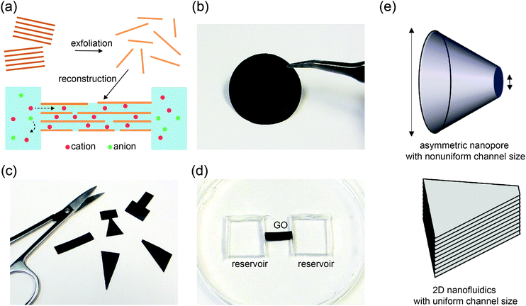 |
| | Fig. 1 Lamellar “paper” as platform for Kirigami nanofluidics. (a) Schematic illustration of the synthesis and assembly of a 2D nanofluidic device. Exfoliated 2D sheets, such as GO, are reconstructed by restacking to form (b) a paper-like thin film with macroscopic dimensions. (c) Different device shapes can be tailor cut from the GO paper. (d) A GO strip is sealed in PDMS with both ends exposed to carved reservoirs for electrolytes. (e) Schematic drawings highlight the microstructural differences between (top) a conical-shaped nanopore, whose channel size is nonuniform and (bottom) a GO film that has uniform channel size, despite of asymmetric macroscopic shape. | |
Results and discussion
Tailor-cut GO films and their I–V curves
Graphene oxide (GO) sheets made by chemical exfoliation of graphite powders are used to construct 2D nanofluidic thin films.20 After purification, the GO solution is filtered under vacuum or drop-cast onto a surface to form a lamellar thin film in which the interlayer spacing constitutes a continuous, interconnected 2D nanofluidic network that supports unipolar ionic transport (Fig. 1a, b and Fig. S1a, ESI†).25 The channel height of GO membranes is tunable via the degree of hydration and has been measured to be around 0.5 to 1.1 nm20,31,32 by X-ray diffraction (Fig. S1b, ESI†). GO paper can be cut into different shapes using scissors (Fig. 1c). The final GO shape is then embedded in polydimethylsiloxane (PDMS) elastomer, and reservoirs for electrolytes are carved out at the two ends of the film (Fig. 1d). Ag/AgCl electrodes are used to apply a voltage across the device and to measure the resulting ionic current. Fig. 1e compares the structure of a conical-shaped nanopore, which represents a prototypical rectifying nanofluidic diodes, to that of a trapezoidal 2D nanochannel film. Although both systems appear to have similarly asymmetric shapes, their microstructures are drastically different. The conical nanopore has asymmetric channel size, thus allowing asymmetric degree of confinement to ions. This can lead to unipolar ionic behavior only near the small end and bulk like behavior near the large end, leading to rectifying ionic current. In contrast, the 2D channels are uniform in height and can support unipolar transport through their entire volume, regardless of the overall shape of the GO film.
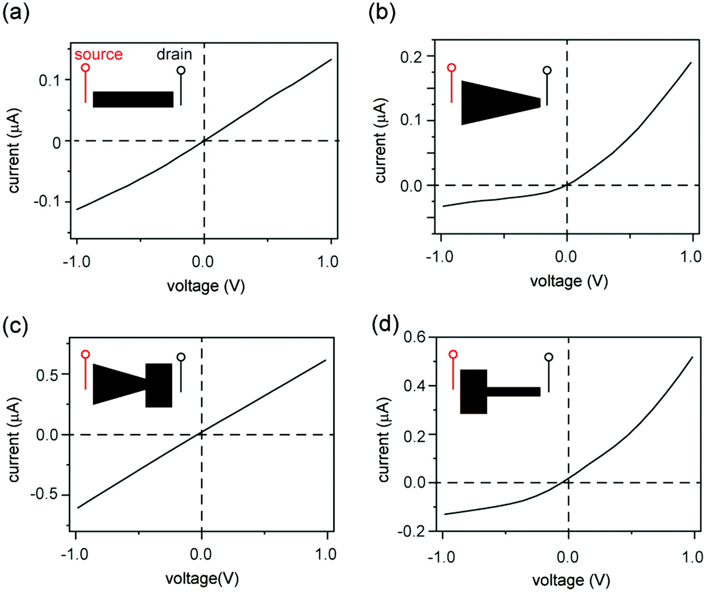
Fig. 2 shows the current–voltage (I–V) curves of films cut into the shape of a rectangle, a trapezoid, a diode sign, and a “T.” For consistency, the working electrode is always placed on the left-hand side of the illustrated GO and is designated as the source. The right side is designated as the drain. The I–V curve measured through a rectangular GO strip (Fig. 2a) is symmetric.20 However, the current through a trapezoidally shaped GO paper is rectified (Fig. 2b), i.e., the forward conductance is higher than the reverse. Multiple I–V sweeps are carried out to confirm reproducibility (Fig. S2, ESI†).
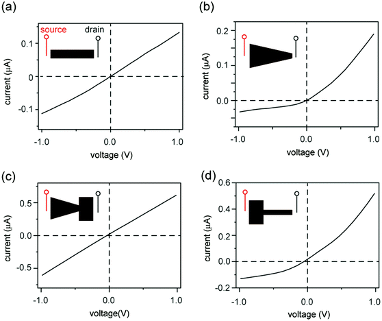 |
| | Fig. 2 Kirigami nanofluidic devices. (a) A rectangular piece of GO paper shows symmetric current under both forward and reverse bias. (b) When cut into a trapezoidal shape, the device rectifies the current, exhibiting typical diode-like behavior. (c) A piece of GO paper with the shape of a “diode sign” does not show rectifying behavior. (d) A T-shaped GO paper shows a diode-like rectifying current. The insets illustrate the top view of the GO papers. For consistency, the left reservoirs of all devices are designated as the source. These results suggest that current rectification is only determined by the relative widths of the two ends, and not by the shape of the GO paper in between. | |
Rectifying mechanism
An explanation for the asymmetric shape induced ionic current rectification observed in Fig. 2a and b, which we proposed earlier33 and others reported subsequently,34 is that the “funnel-like” shape of the trapezoid leads to the accumulation of charge carriers (i.e., cations) inside the GO channels when carriers migrate from the wider to the narrower end under forward bias, and leads to depletion of charge carriers under reverse bias. Although this “accumulation–depletion” argument explains ionic rectification in many other types of nanofluidic systems,18 such as conical-shaped pores (Fig. 1e, top), we have now realized that it is fundamentally incompatible with the structure of the GO membrane and violates electroneutrality. Due to its asymmetric channel size, a rectifying conical nanopore is only partially charge selective (e.g., near the smaller end) and can allow both cations and anions to accumulate and deplete near the larger end of the channel, where ions exhibit bulk transport behaviors. In contrast, the 2D nanofluidic system has uniform channel size (Fig. 1e, bottom) and is entirely charge selective. Therefore, the concentration of the main charge carrier (i.e., cations) should not fluctuate because it is determined by the surface charge density of the GO sheets. Applying the “accumulation–depletion” mechanism to these particular 2D nanochannels would thus violate electroneutrality. In addition, the accumulation–depletion argument would predict that a “diode-sign” shape (Fig. 2c, inset), in which the “bottle neck” (i.e., the narrow end of the funnel) is placed toward the drain, should act as a rectifier as well (see scheme and analysis in Fig. S3, ESI†). However, its I–V curve (Fig. 2c) is symmetric. Lastly, we examined a GO paper cut into the shape of a “T,” and found that it also acted as a rectifier (Fig. 2d). The fact that shapes with asymmetric sizes of source and drain (i.e., the trapezoid and the “T”) rectify and asymmetric shapes with symmetric ends (e.g., the rectangle and the “diode sign”) do not suggests that rectification should be determined only by the relative sizes of the reservoir-end interfaces.
Concentration polarization
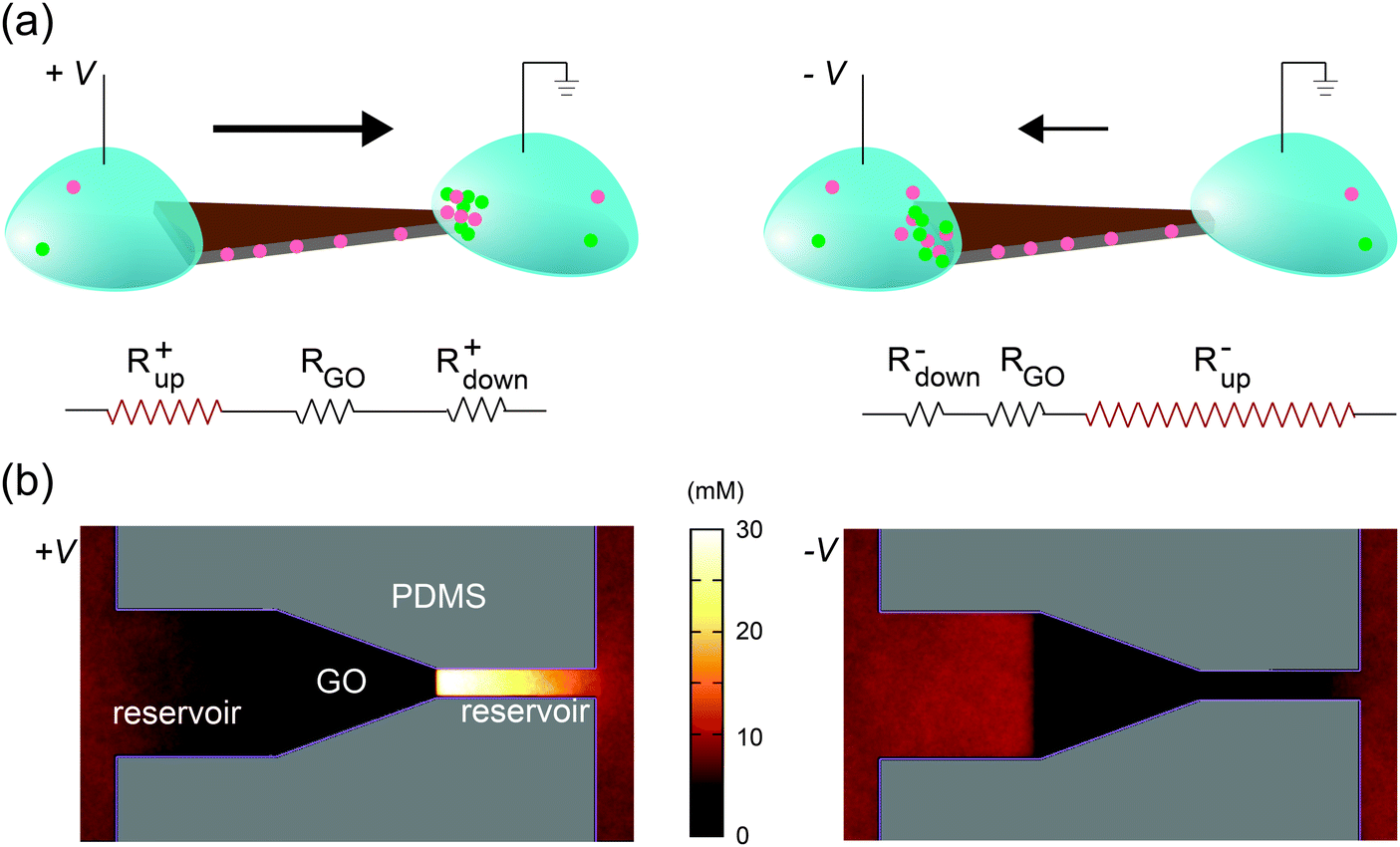
Selective transport of ions or molecules through a medium results in the development of concentration gradients near both interfaces; the transporting species is depleted on the upstream side and enriched at the downstream side. This phenomenon is generic for any molecularly selective membrane, and is often labeled concentration polarization (CP).35–38 As described below, we found that the rectified ionic currents observed in Fig. 2b and d are simply due to the asymmetric depletion in the CP zones at the source and drain sides, which is directly determined by their edge lengths. An intuitive explanation is illustrated in Fig. 3a, using the trapezoid as an example. The total ionic resistance of the system consists of five terms in series: the two reservoirs, the two channels–reservoir interfaces (i.e., CP zones), and the lamellar nanochannels themselves (circuit diagram in Fig. 3a). The resistance of each section is inversely related to its width and its carrier concentration. The resistances of the macroscopic reservoirs are insignificant. The resistance of the GO nanochannel network is constant since the carrier concentration in the channels is fixed by the GO surface charge. Since the CP effect on the downstream side leads to the enrichment of ions, the resistance of the downstream interface is relatively insignificant. However, ions are depleted at the upstream interface, and this removal of charge carriers yields a high resistance. Therefore, even at relatively low voltages the overall resistance is dominated by the resistance of the channel–reservoir interface on the upstream side. For shapes with symmetric source and drain (Fig. 2a and c), the overall resistances are obviously the same under forward and reverse bias. However, for shapes with asymmetric interfacial widths such as the trapezoid, their wider edge is upstream under forward bias (Fig. 3a, left) whereas their narrower edge is upstream under reverse bias (Fig. 3a, right). Since the CP-zone resistance at the narrower edge is larger than that at the wider edge, the forward current is higher than the reverse current.
 |
| | Fig. 3 Rectification mechanism. (a) Due to CP, ions are depleted at the upstream interface, leading to high upstream resistance Rup. On the other hand, the resistance at the downstream interface (Rdown), where ions are enriched, is relatively insignificant. The resistance through the GO channels (RGO) is constant. Under forward bias (+V), the upstream side is located on the left, which has larger width and thus lower Rup. Under reverse bias (–V), the upstream interface is on the right, which has narrower width and larger Rup. This explains current rectification in the trapezoidally shaped device. (b) Top view of the anionic concentration profile obtained in molecular dynamics simulations of the trapezoidal GO film and its reservoirs. Note the clear difference in the ionic concentration profile between forward (left) and reverse (right) bias, in agreement with (a). To accurately capture the quasi-one-dimensional shape of the CP zones in the experimental device, two artificial “channels” are added at the two ends in simulation (see Experimental section and ESI,† Note 2 for details). | |
This qualitative explanation is demonstrated mechanistically by molecular dynamics simulations, which confirm the existence of CP regions that dominate the overall resistance of the system. In these simulations, a GO nanochannel network is immersed in an electrolyte consisting of explicit ions and implicit solvent, and the system is allowed to reach steady state under an applied voltage bias (see Experimental section). The ion concentration shows asymmetric CP under forward and reverse biases (Fig. 3b) in qualitative agreement with Fig. 3a, leading to asymmetric ionic current upon voltage reversal. The relationship between the rectification ratio and the geometrical asymmetry is consistent between simulation and experiment, and supports the proposed mechanism. As far as this mechanism is concerned, the channel conductance, depletion-zone length, ion concentrations, and system size are only important in relation to one another, and therefore the differences of these values between simulation and experiment can be ignored. Previously, it has been observed that asymmetric CP zones can induce rectification through a single layer of nanofluidic channels, but only when extremely high electrical field is applied (>104 V m−1).9 By contrast, in our system, rectification starts at around 10 V m−1 (see Fig. 2). This drastic difference highlights one key advantage of the 2D nanochannels – their scalability. For a single or small array of nanofluidic channels, the resistance attributed to the CP zones becomes significant only when they are deeply depleted under high electrical field. Since the lamellar film used here contains massive arrays of parallel 2D channels, the effect of CP zones becomes much more pronounced and is readily observed at very low voltage (Fig. S4, ESI,† Note 1).
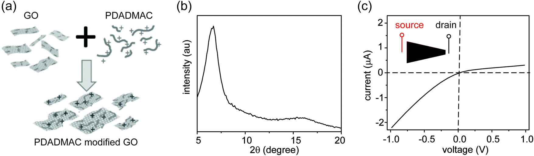
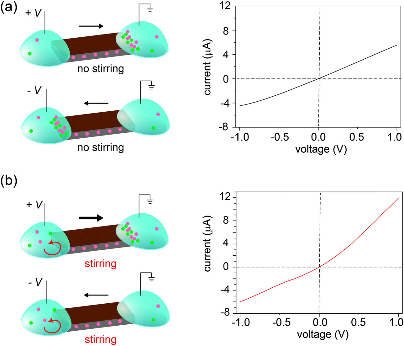
Three control experiments were conducted to verify the proposed mechanism, each designed to manipulate the CP zones at the two interfaces. First, we increased the electrolyte concentration beyond the regime where surface charge dominates the ion concentration (e.g., around 50 mM),20 such that the nanochannels lose their cation selectivity. Under this condition, we do not expect CP zones to develop and ionic current rectification should not occur, even for a film with an asymmetric shape. Fig. S5, ESI† confirms that the trapezoid no longer rectifies at an electrolyte concentration of 50 mM. Second, if the charges on the nanochannels are reversed, the film becomes anion selective, so that the polarity of the rectifier should reverse as well. This is verified in Fig. 4, where the surface charge of GO is rendered positive by modification with a positively charged polyelectrolyte. Lastly, our qualitative explanation implies that the current will be rectified whenever the CP zone at the two ends of the GO paper is asymmetric in shape or size, even if the paper itself has a symmetric shape. For example, by selectively stirring only one reservoir to manipulate the CP zone39 in an asymmetric manner, rectification can even be induced in a rectangular strip of GO paper. Without stirring, the I–V curve of the rectangular strip is symmetric (Fig. 5a), but when the source reservoir is stirred, the depleted zone can only build up at the drain-side interface. Consequently, the rectangular strip exhibits rectified ionic current with higher resistance under reverse bias due to ionic depletion at the drain-side interface (Fig. 5b). These control experiments confirm that rectification is determined by the depletion-induced resistances of the two interfaces, a simpler mechanism than those of prior studies regarding nanofluidic diodes.9 Transiently asymmetric CP zones can also be observed in a rectangular strip in the course of a fast I–V scan, as one half of the scan experiences more fully developed CP than the other.38,40
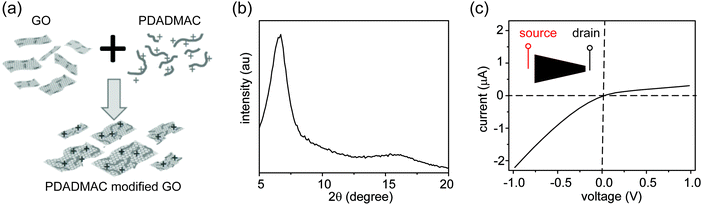 |
| | Fig. 4 Rectification direction is reversed when surface charge is reversed. (a) GO sheets (1 mg mL−1 in water) are modified with positively charged polyelectrolyte poly(diallyldimethylammonium chloride) (PDADMAC, 1 mg mL−1 in water). (b) XRD pattern of PDADMAC-modified GO film in dry state. The d-spacing is 1.3 nm, larger than that of GO. (c) I–V curve recorded through a trapezoid nanofluidic device made from PDADMAC-modified GO film, showing that the rectification direction is reversed. | |
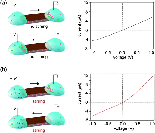 |
| | Fig. 5 Disrupting CP zones by stirring. (a) For a rectangular GO strip, the CP zones are symmetric under both biases leading to a symmetric I–V curve. (b) Stirring the left reservoir selectively suppresses the formation of CP resulting in current rectification. | |
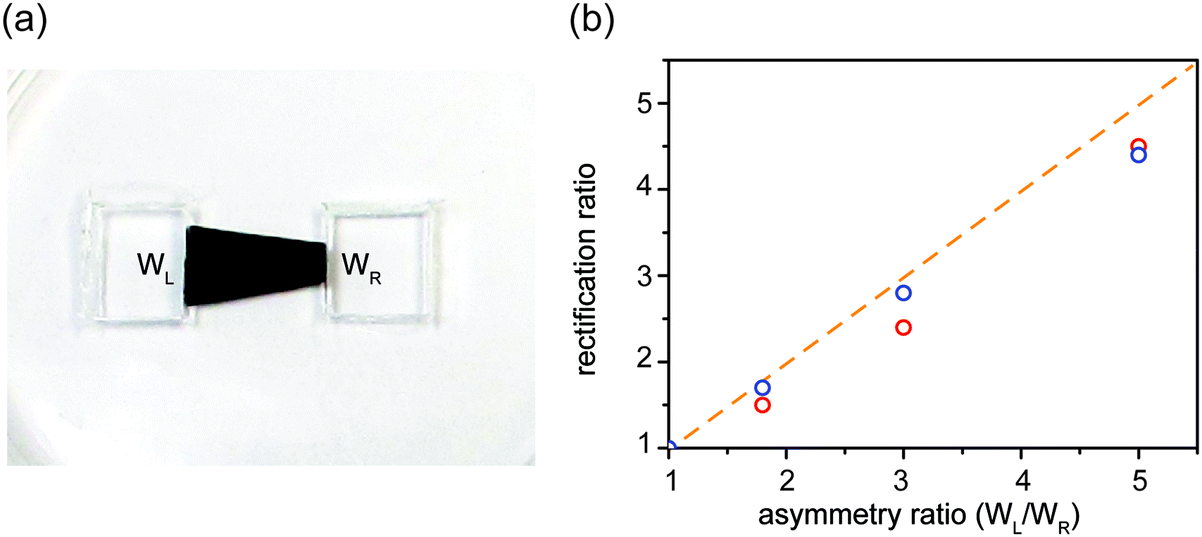
Tuning rectification ratio
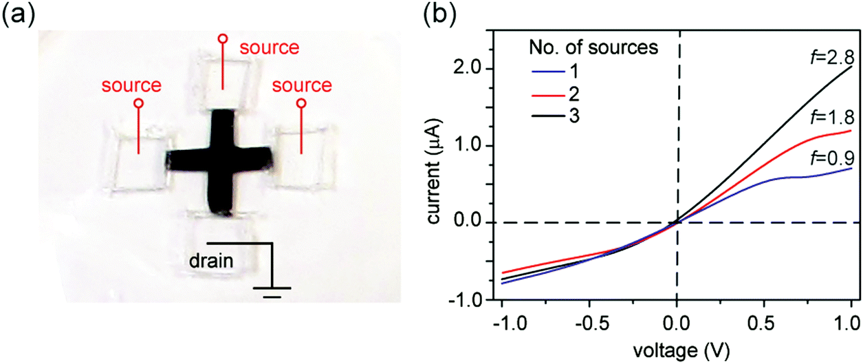
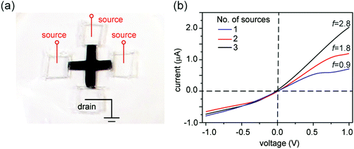
Since asymmetric source and drain widths lead to ionic rectification (Fig. 2), we investigate whether altering the width ratio of the lamellar film on the source and drain sides by, e.g., cutting the film into different shapes, can tune the rectification ratio f. Indeed, for the trapezoidal shapes, we found that f is close to the ratio of the edge widths, in close agreement with molecular dynamics simulations (Fig. 6). Another strategy is to cut membranes into shapes with multiple branches with equal edge widths, and select an asymmetric number of branches for the source and the drain to induce ionic current rectification. Fig. 7 shows the results obtained with a cross-shaped GO paper with four equally sized branches. In this experiment, one branch is used as drain, while the number of branches used as source is varied from 1 to 3 (Fig. 7a). The I–V curves in Fig. 8b show the measured rectification ratios. With 1, 2, or 3 source branches, the corresponding values of f are 0.9, 1.8, and 2.8, respectively, scaling as anticipated. Note that the currents at negative voltages are similar for all three cases, consistent with the finding that the depleted, upstream interface of the device dictates the resistance of the system.
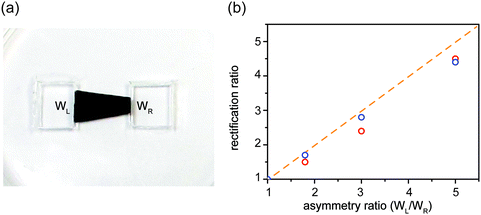 |
| | Fig. 6 Rectification ratio determined by the asymmetry ratio of edge widths. (a) A trapezoidal GO nanofluidic diode with left-side width of WL and right-side width of WR. If the GO membrane resistance is neglected, the rectification ratio is expected to equal asymmetry ratio. (b) The measured (red circles) and molecular-dynamics calculated (blue circles) rectification ratio is closely related to the asymmetry ratio (WL/WR). An eye-guide (orange dashed line) is drawn to represent rectification ratio = WL/WR. | |
 |
| | Fig. 7 Programming the rectification ratio. (a) Photo showing a cross-shaped GO paper with four branches. One branch is designated as the drain. By varying the number of branches that are connected to the source, the rectification ratio f can be tuned. (b) Current–voltage measurements show that the forward current varies in direct proportion to the number of source branches used. The reverse-voltage resistance is determined mostly by the edge length of the drain end and therefore remains largely unchanged. | |
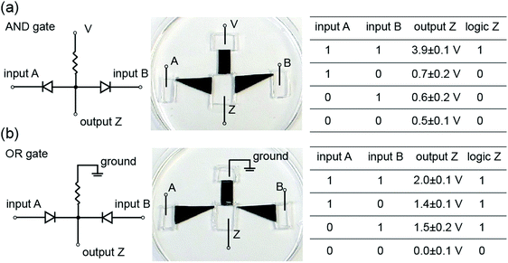 |
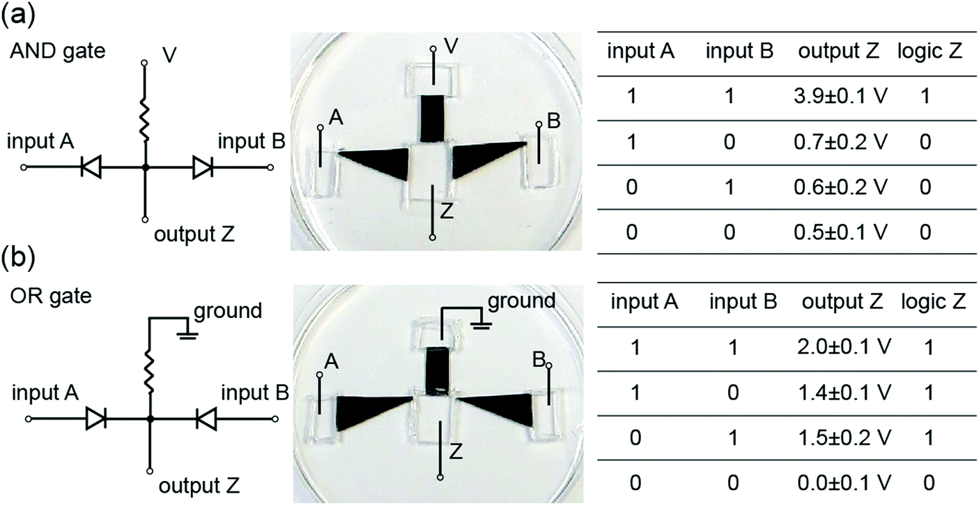
| | Fig. 8 Ionic logic functions. (a and b) show, from left to right, the circuit diagrams, device photos, and truth tables of the AND and OR logic functions, respectively. The input high and low voltages are 4 V and 0 V, respectively. For both cases, a clear difference between logical 1 and 0 states is observed. | |
Connecting nanofluidic components
Kirigami-nanofluidic components are modular and can therefore easily be assembled into more complex ionic circuits such as logic gates (Fig. 8). The output voltages for both gates exhibit a significant and clearly distinguishable difference between the logical 1 and 0 states, and the logic values are in agreement with corresponding logic algorithms. It should be noted that our devices are a proof of concept, and high-performance logic gates would require the output high and low voltage to be nearly equal to the input high and low voltage, respectively. These elementary forms of logic circuits serve to illustrate some possible new functions by connecting Kirigami made nanofluidic elements. The development of actively switchable GO nanofluidic components is needed for achieving ionic computing functions and circuitry.
Conclusions
We have demonstrated a material platform supporting 2D nanofluidics that is simple to fabricate and has consistent nanoscopic channel height through its macroscopic dimensions. This allows much simpler control over ionic transport, as demonstrated by Kirigami-nanofluidic diodes and circuits. Ionic current rectification in such 2D nanofluidic systems can be accomplished without the need for precise microfabrication, but instead by conveniently tailor-cutting the shape of the lamellar films. Our experiments and calculations demonstrate that asymmetric edge lengths lead to asymmetric interfacial resistances in the concentration-polarization zones under forward and reverse bias, resulting in ionic current rectification. By fine-tuning the transport properties as well as computer-assisted patterning,41 it should be feasible to realize continuous ionic manipulation including sieving, separation, and information processing on a single film.
Experimental
GO is fabricated via modified Hummer's method42 and then purified via two-step washing as reported previously.43 Vacuum filtration or the drop-cast method is used to obtain GO paper. The GO paper is typically 10 to 20 μm thick. Prior to embedding in PDMS precursor, the GO papers are cut into different shapes using scissors. Subsequently, the PDMS is cured at 70 °C for 1 h and then two electrolyte reservoirs are carved out to expose the two ends of the GO film. The fabricated device is then immersed in deionized water overnight to ensure complete hydration. Before ionic current measurement, the device is further immersed in testing electrolyte for at least 8 h to ensure stable conductance. Here the testing electrolyte is KCl at bulk concentration 10−4 M in water unless specified otherwise. Ionic current is recorded by a Keithley 2601A source meter with two Ag/AgCl electrodes. Ag/AgCl electrodes were tested before each experiment, by placing both electrodes in one reservoir and recording IV curves, and only used for experiments when the curve was Ohmic. For device tests, the scan speed was typically between 10−2 and 10−4 V s−1, so that relatively consistent ionic currents can be obtained. It is expected that at this range of scanning rate, near-steady state CP zones can be developed without significantly altering the overall ionic concentrations in the reservoirs. Rectification ratio is calculated by dividing the current at +1 V by the current at −1 V. The GO strips used in this work are typically 1–2 cm in length and the volume of reservoirs is typically 0.5–2 mL. The range of suitable scanning rate may need to be adjusted for systems with significantly different channel lengths or reservoir sizes. For logic circuits, a Keithley 2400 source meter is used to provide input voltages. More details regarding device fabrication and measurement can be found in our previous work.20
Molecular dynamics simulations are performed of ions in confined geometries, embedded in an implicit solvent. The ions are placed in a periodically replicated 350 nm × 200 nm × 4.98 nm simulation box. The length of the box is divided into a 50 nm bulk region, a 100 nm GO region, and two 100 nm-long “channel” regions that connect the GO to the bulk, which are the widths of the GO–reservoir interfaces (Fig. 3b). These channel regions were required to prohibit radial focusing9 and therefore capture the quasi one-dimensional geometry that emerges at the interface of thousands of stacked nanochannels (see ESI,† Note 1). The external field is applied along the x-direction. A set of repulsive walls represents the PDMS barricades and restricts ions from crossing the box boundaries in the y- and z-directions. The excluded volume of the GO sheets is modeled by a set of parallel, repulsive planes that are normal to the z-axis and separated by 1.66 nm in the z-direction. The surface charge of GO is modeled by embedding monovalent charges at a surface density of 0.046 e− nm−2, near the upper range for GO.20 The area of the GO trapezoid is kept at a constant 11![[thin space (1/6-em)]](https://www.rsc.org/images/entities/char_2009.gif) 000 nm2 for all geometric asymmetries. Simulations were performed with the bulk concentration fixed at 7.6 mM.
000 nm2 for all geometric asymmetries. Simulations were performed with the bulk concentration fixed at 7.6 mM.
Conflicts of interest
There are no conflicts to declare.
Acknowledgements
This work was partially supported by a seed grant from the Materials Research Science and Engineering Centers (MRSEC) program at Northwestern University (NSF DMR-1121262). J. H. acknowledges additional support from the Office of Naval Research (N000141310556, then N000141612838).
Notes and references
- D. Stein, M. Kruithof and C. Dekker, Phys. Rev. Lett., 2004, 93, 035901 CrossRef PubMed.
- L. Bocquet and E. Charlaix, Chem. Soc. Rev., 2010, 39, 1073–1095 RSC.
-
P. Abgrall and N.-T. Nguyen, Nanofluidics, Artech House, Boston, 2009 Search PubMed.
- R. B. Schoch, J. Y. Han and P. Renaud, Rev. Mod. Phys., 2008, 80, 839–883 CrossRef CAS.
- W. Sparreboom, A. van den Berg and J. C. T. Eijkel, Nat. Nanotechnol., 2009, 4, 713–720 CrossRef CAS PubMed.
-
C. Kittel, Introduction to solid state physics, Wiley, Hoboken, NJ, 8th edn, 2005 Search PubMed.
- J. Goldberger, R. Fan and P. Yang, Acc. Chem. Res., 2006, 39, 239–248 CrossRef CAS PubMed.
- R. Fan, S. Huh, R. Yan, J. Arnold and P. D. Yang, Nat. Mater., 2008, 7, 303–307 CrossRef CAS PubMed.
- G. Yossifon, Y.-C. Chang and H.-C. Chang, Phys. Rev. Lett., 2009, 103, 154502 CrossRef PubMed.
- W. H. Guan, R. Fan and M. A. Reed, Nat. Commun., 2011, 2, 506 CrossRef PubMed.
- K. Tybrandt, E. O. Gabrielsson and M. Berggren, J. Am. Chem. Soc., 2011, 133, 10141–10145 CrossRef CAS PubMed.
- K. Tybrandt, K. C. Larsson, A. Richter-Dahlfors and M. Berggren, Proc. Natl. Acad. Sci. U. S. A., 2010, 107, 9929–9932 CrossRef CAS PubMed.
- K. Tybrandt, R. Forchheimer and M. Berggren, Nat. Commun., 2012, 3, 871 CrossRef PubMed.
- X. Hou, W. Guo and L. Jiang, Chem. Soc. Rev., 2011, 40, 2385–2401 RSC.
- H. Daiguji, Y. Oka and K. Shirono, Nano Lett., 2005, 5, 2274–2280 CrossRef CAS PubMed.
- I. Vlassiouk and Z. S. Siwy, Nano Lett., 2007, 7, 552–556 CrossRef CAS PubMed.
- R. Yan, W. Liang, R. Fan and P. Yang, Nano Lett., 2009, 9, 3820–3825 CrossRef CAS PubMed.
- L. J. Cheng and L. J. Guo, Chem. Soc. Rev., 2010, 39, 923–938 RSC.
- L.-J. Cheng and L. J. Guo, Nano Lett., 2007, 7, 3165–3171 CrossRef CAS PubMed.
- K. Raidongia and J. Huang, J. Am. Chem. Soc., 2012, 134, 16528–16531 CrossRef CAS PubMed.
- W. Guo, C. Cheng, Y. Wu, Y. Jiang, J. Gao, D. Li and L. Jiang, Adv. Mater., 2013, 25, 6064–6068 CrossRef CAS PubMed.
- W. Guo and L. Jiang, Sci. China Mater., 2014, 57, 2–6 CrossRef.
- J. J. Shao, K. Raidongia, A. R. Koltonow and J. Huang, Nat. Commun., 2015, 6, 7602 CrossRef PubMed.
- C. Cheng, G. Jiang, C. J. Garvey, Y. Wang, G. P. Simon, J. Z. Liu and D. Li, Sci. Adv., 2016, 2, e1501272 Search PubMed.
- A. R. Koltonow and J. Huang, Science, 2016, 351, 1395–1396 CrossRef CAS PubMed.
- S. Qin, D. Liu, G. Wang, D. Portehault, C. J. Garvey, Y. Gogotsi, W. Lei and Y. Chen, J. Am. Chem. Soc., 2017, 139, 6314–6320 CrossRef CAS PubMed.
- S. Wu, F. Wildhaber, O. Vazquez-Mena, A. Bertsch, J. Brugger and P. Renaud, Nanoscale, 2012, 4, 5718–5723 RSC.
- E. A. Jackson and M. A. Hillmyer, ACS Nano, 2010, 4, 3548–3553 CrossRef CAS PubMed.
- W. Ouyang, J. Han and W. Wang, Lab Chip, 2017, 17, 3006–3025 RSC.
- E. Choi, C. Wang, G. T. Chang and J. Park, Nano Lett., 2016, 16, 2189–2197 CrossRef CAS PubMed.
- D. A. Dikin, S. Stankovich, E. J. Zimney, R. D. Piner, G. H. B. Dommett, G. Evmenenko, S. T. Nguyen and R. S. Ruoff, Nature, 2007, 448, 457–460 CrossRef CAS PubMed.
- A. Lerf, A. Buchsteiner, J. Pieper, S. Schöttl, I. Dekany, T. Szabo and H. P. Boehm, J. Phys. Chem. Solids, 2006, 67, 1106–1110 CrossRef CAS.
- J. X. Huang, Abstr. Pap. Am. Chem. S., 2014, 247, 1 Search PubMed.
- S. T. Martin, A. Neild and M. Majumder, APL Mater., 2014, 2, 092803 CrossRef.
-
R. F. Probstein, in Physicochemical Hydrodynamics, John Wiley & Sons, Inc., 2005 Search PubMed.
- S. J. Kim, Y.-C. Wang, J. H. Lee, H. Jang and J. Han, Phys. Rev. Lett., 2007, 99, 044501 CrossRef PubMed.
- S. Ilias and R. Govind, Sep. Sci. Technol., 1990, 25, 1307–1324 CrossRef CAS.
- M. Miansari, J. R. Friend, P. Banerjee, M. Majumder and L. Y. Yeo, J. Phys. Chem. C, 2014, 118, 21856–21865 CAS.
- M. C. Porter, Ind. Eng. Chem. Prod. Res. Dev., 1972, 11, 234–248 CAS.
- M. Miansari, J. R. Friend and L. Y. Yeo, Adv. Sci., 2015, 6, 1500062 CrossRef PubMed.
- W. Gao, N. Singh, L. Song, Z. Liu, A. L. M. Reddy, L. Ci, R. Vajtai, Q. Zhang, B. Wei and P. M. Ajayan, Nat. Nanotechnol., 2011, 6, 496–500 CrossRef CAS PubMed.
- W. S. Hummers and R. E. Offeman, J. Am. Chem. Soc., 1958, 80, 1339 CrossRef CAS.
- F. Kim, J. Luo, R. Cruz-Silva, L. J. Cote, K. Sohn and J. Huang, Adv. Funct. Mater., 2010, 20, 2867–2873 CrossRef CAS.
Footnotes |
| † Electronic supplementary information (ESI) available. See DOI: 10.1039/c7qm00620a |
| ‡ Present address: Department of Chemistry, Indian Institute of Technology Guwahati, Guwahati, Assam 781039, India. |
| § Present address: Department of Chemistry, Lund University, Lund, Sweden. |
|
| This journal is © the Partner Organisations 2018 |
Click here to see how this site uses Cookies. View our privacy policy here. 
 a,
B.
Beckerman
a,
N.
Boon§
a,
B.
Beckerman
a,
N.
Boon§