
Electronic properties of tin iodide hybrid perovskites: effect of indium doping
Keisuke
Kobayashi†
a,
Hiroyuki
Hasegawa‡
 *b,
Yukihiro
Takahashi
ab,
Jun
Harada
ab and
Tamotsu
Inabe
*ab
*b,
Yukihiro
Takahashi
ab,
Jun
Harada
ab and
Tamotsu
Inabe
*ab
aGraduate School of Chemical Science and Engineering, Hokkaido University, Kita 10 Nishi 8, Kita-ku, Sapporo 060-0810, Japan. E-mail: inabe@sci.hokudai.ac.jp
bFaculty of Science, Hokkaido University, Japan. E-mail: hhase@nict.go.jp
First published on 22nd March 2018
Abstract
Indium doping is introduced to tune the electronic properties of tin iodide hybrid perovskites. By applying this method, the resistivity of tin-iodide-based hybrid perovskites is reduced using indium doping without any change in its band gap. This mixed tin/indium iodide crystal perovskite is obtained using a solution process. The resistivity of the materials continuously increased from 10−2 to 10−1 Ω cm at room temperature, even when the doping level was less than 22 ppm. The metallic nature of this system decreased with increasing doping level, while the carrier density did not vary with the doping level. This method of foreign metal doping provides resistivity control of the tin iodide hybrid cubic perovskites without changing the band gap or carrier concentration.
Introduction
The electronic structure of organic–inorganic hybrid perovskite compounds can be controlled using solution processes. Remarkable progress has been achieved for such compounds, especially for metal halide cubic perovskites for solar cells.1–11 To enhance the efficiency of these devices, it is essential to control the electronic structure and functions of the material.Band engineering is one method to control the electronic structure.12–14 For example, the width of the band gap in light-emitting diodes is the dominant factor controlling the emitting wavelength; hence, the band gap of the semiconductor must correspond to the desired wavelength. The band gap of GaN corresponds to the ultraviolet region; therefore, it cannot be used as a blue-emitting diode. However, InN, which has a narrower band gap, can be used to form a mixed (In,Ga)N crystal with GaN, and the band gap can be adjusted to meet the energy for blue-light emission. This kind of band gap adjustment is available for inorganic compounds and organic–inorganic hybrid perovskites. We previously reported a method for the band gap reduction of a tin-iodide-based organic–inorganic hybrid perovskite by doping with a small amount of bismuth.15
The parent materials of organic–inorganic tin iodide perovskites (Fig. 1) are known as not only alternative materials for lead-based perovskite solar cells16–24 but also exceptionally conductive materials in hybrid perovskites. We reported that the highly conductive nature of these perovskites originates from the unintended spontaneous carrier doping by the Sn(IV) content.25 A cubic crystal of CH3NH3SnI3 exhibits metallic behavior in terms of the temperature dependencies of the conductivity and thermoelectric power even though it has a band gap of 1.3 eV. A Hall effect measurement revealed that the doping level of this material is 0.02%. Therefore, we concluded that this material is a doped semiconductor.26 Furthermore, we demonstrated that the artificial doping of Sn(IV) increased the doping level of the material. The majority carriers were holes originating from Sn(IV). This crystal can also be dedoped using a significantly excess amount of a reductant.27 Consequently, the tin iodide perovskite has a semiconducting band structure, though the doping level depends on the sample preparation conditions.
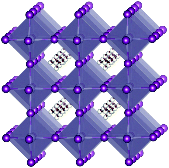 | ||
| Fig. 1 Cubic perovskite structure. The SnI6 octahedra are hatched. The methylammonium cations at interstitial “A” sites are disordered. | ||
Herein, we report another attempt of foreign metal (indium) doping into a tin iodide perovskite. As seen in indium tin oxide, indium has a good affinity with tin. In indium oxide, which is an insulator, the bottom of the conduction band consists of the 5s orbital of indium.28 When tin atoms are doped, impurity states of Sn and voids form just below the bottom of the conduction band. In a highly doped state, these states form a band and lower the bottom of the conduction band,29,30 thereby increasing the conductivity. We present the effect of indium doping on the electronic transport, structural, and optical characteristics of tin iodide hybrid cubic perovskite bulk crystals.
Experimental details
Crystal preparation
A previously reported procedure for preparing a foreign-metal-doped cubic perovskite15 was applied for indium doping. A stoichiometric ratio of tin(II) iodide (Kojundo Chemical Laboratory Co., Ltd) and indium(I) iodide (Aldrich) was added to one side of an H-shaped glass tube. Methylammonium iodide was added to the other side. Then, hydroiodic acid was added separately into the tube by distillation under inert conditions. The mixture was heated to 80 °C to dissolve the metal iodides and methylammonium iodide. Then, the two solutions were mixed in the tube. Perovskite crystals were obtained as the solution slowly cooled. The chemical compositions of these crystals were determined using a Shimadzu ICPE-9000 inductively coupled plasma emission spectrometer.X-ray diffraction
Powder X-ray diffraction data were recorded using a D8 ADVANCE diffractometer (Cu Kα radiation) and were analyzed by performing profile fitting based on the Pawley method using TOPAS 4.2 software. All measurements were performed at room temperature.Electronic properties
Diffuse reflectance spectra were recorded using a JASCO V-570 UV/VIS/NIR spectrometer with an integrating sphere unit. The samples were ground with KBr. The reflectivity was converted to the Kubelka–Munk function (KM) corresponding to the absorption, and then normalized.The temperature dependence of the conductivity was measured using a Keithley 2636A dual-channel SourceMeter. The sample was placed in a cryostat controlled by a Scientific Instruments 9700 temperature controller. The data were recorded using custom-written software. Measurements were performed using a standard four-probe method under vacuum conditions. A carbon paste (Dotite XC-12, Fujikura Kasei Co., Ltd) was used to mount four gold wires. The original thinner (toluene) in the carbon paste was partially evaporated by a stream of N2 gas, and then tetralin (1,2,3,4-tetrahydronaphthalene) was added to the paste as a thinner.
Thermoelectric power measurements were performed via a method based on that reported by Chaikin and Kwak,31 using a Keithley 2182 nanovoltmeter and Advantest R6243 DC voltage current source/monitor. The samples were mounted at the gap between two gold foils using the same carbon paste used for the conductivity measurements.
Results and discussion
Indium was successfully doped into methylammonium tin iodide perovskite via an energy-saving solution process. The indium contents were determined by inductively coupled plasma emission spectroscopy. The compositional ratio of indium (δ) in the mixed crystal of CH3NH3Sn1−δInδI3 increased upon increasing the starting molar ratio during sample preparation (Table 1); however, the efficiency of indium doping was less than that of bismuth doping.15 There is no significant difference in chemical stability between the as-grown and the indium-doped crystals. The powder X-ray diffraction data of the doped sample indicated that the cubic structure of the tin iodide perovskite was not significantly affected by indium doping (Fig. 2). The estimated lattice parameter of the doped crystal is 6.23582(22) Å, which is almost the same as that of the as-grown crystal (6.23176(33) Å); therefore, the basic structure of the cubic crystal was maintained.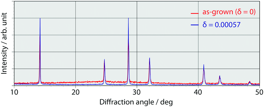 | ||
| Fig. 2 Powder diffraction patterns of In-doped and as-grown (i.e., without In doping) CH3NH3SnI3. | ||
Diffuse reflectance spectra for various indium contents (Fig. 3) revealed that the band gap of the perovskite was not affected by indium doping. As reported previously, the band gap for the as-grown crystal (δ = 0) is 1.3 eV; however, there is a deviation in the near-IR region due to low-energy excitation of charge carriers.26 The band gaps of the mixed crystals were independent of the indium doping ratios. When the influence of indium doping on the band gap is considered based on the standard electrode potential values of In and Sn (Sn/Sn2+: −0.14 V, In/In+: −0.34 V),32–34 the 5p orbital of tin, which forms the bottom of the conduction band, has a higher potential than indium; this is consistent with our previous discussion on bismuth doping. Therefore, indium doping should lower the bottom of the conduction band. However, such an effect was not observed at any of the examined indium doping ratios. The band gap did not change within the same range of doping ratios for bismuth doping; therefore, the conduction band was not lowered because the indium content was too low.
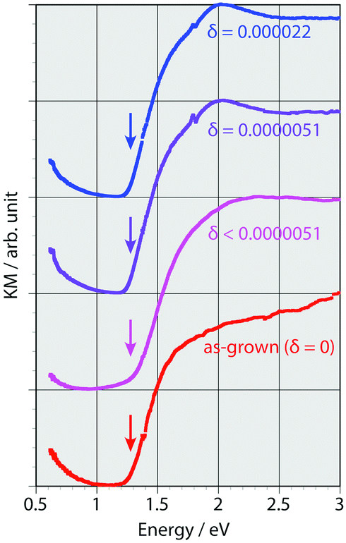 | ||
| Fig. 3 Diffuse reflectance spectra of indium-doped tin iodide cubic perovskites with various amounts of doping. The arrows indicate the band gaps. | ||
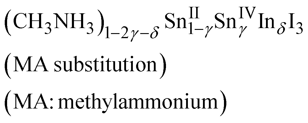
Indium doping also affected the electronic properties. For the as-grown crystal (δ = 0), the band structure was the same as that of an intrinsic semiconductor, though that is a doped semiconductor due to the spontaneous doping effect. Therefore, the temperature dependence of the resistivity shows metallic behavior due to the holes injected at the top of the valence band by spontaneous doping. Fig. 4 shows the temperature dependence of the resistivity and that of the thermoelectric power for different values of δ. The resistivity increases with increasing doping ratio; metallic behavior is observed at all doping ratios. However, the slopes in the low temperature region become less steep at higher doping ratios. Sn(IV) atoms were included in the as-grown crystal (δ = 0), corresponding to 0.02% holes. Doping of iodide ions can balance the electrical neutrality; otherwise, Sn(II) or methylammonium ion defects can occur. The as-grown crystal shows clear metallic behavior in terms of resistivity until low temperatures were reached; it would be more difficult to affect the crystal structure and conductivity without breaking the Sn–I framework. Therefore, the composition (CH3NH3)1−2γSnII1−γSnIVγI3 with methylammonium defects is suitable here; however, the defect formation energy calculation indicates that Sn(II) defection is appropriate for the discussion of CsSnI3.35
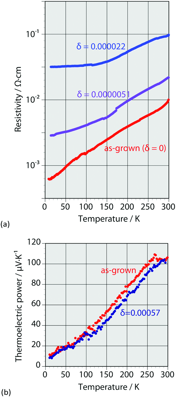 | ||
| Fig. 4 (a) Temperature dependence of the resistivity of indium-doped tin iodide single crystals with various amounts of doping. (b) The temperature dependence of the thermoelectric power for the In-doped and as-grown (i.e., without In doping) CH3NH3SnI3 single crystals. | ||
The slopes of the thermoelectric power behaviors of the as-grown and doped crystals indicate that their Fermi levels are almost the same. Therefore, the carrier concentrations in the indium-doped crystals are also the same. Furthermore, the chemical compositions of the doped crystals change to the following compositions based on electrical neutrality:
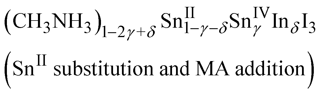 | (1) |
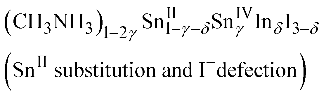 | (2) |
 | (3) |
The slope for the temperature dependence of the resistivity in the low temperature region becomes less steep with increasing indium content; this behavior differs from that reported for bismuth doping. The structural change of the Sn–I framework is closely related to the carrier conduction in the doped crystals. Thus, composition (2), which includes I− defection, is likely the appropriate composition to represent indium doping into methylammonium tin iodide perovskite at this stage. Further investigation of highly doped samples will help elucidate this situation.
Consequently, we found that indium doping reduces the conductivity without changing the band gap or carrier concentration. The mobility of the doped crystals decreased because there was no change in the carrier concentration. This effect likely originates from the change in the Sn–I framework caused by indium doping.
Conclusions
For solution-processable tin iodide cubic perovskites, a small amount of indium doping reduced the conductivity without changing the band gap or the carrier concentration. In band engineering, the doped metal needs to be well matched with the parent crystal lattice to control the physical properties. However, it is difficult to predict the controllability of the physical properties by the dopant. From such a viewpoint, our research will give useful information on foreign metal doping in the hybrid perovskites. We demonstrated another possibility of foreign metal doping in tin iodide cubic perovskites and displayed a design strategy for electronic devices using hybrid perovskites, such as solar cells and light-emitting diodes. More highly efficient devices are expected to be developed using this strategy.Conflicts of interest
There are no conflicts to declare.Acknowledgements
The authors express their gratitude toward Prof. Atsushi Kobayashi and Prof. Masako Kato (Hokkaido University) for their guidance in conducting the powder X-ray diffraction experiments. This work was mainly supported by the CREST program of the Japan Science and Technology Agency (JST), and partially supported by a research grant awarded by the Support Center for Advanced Telecommunications Technology Research Foundation (SCAT), Japan, and Grants-in-Aid for Scientific Research of the Japan Society for the Promotion of Science (JSPS) (17H05170 and 17K06037).Notes and references
- A. Kojima, K. Teshima, Y. Shirai and T. Miyasaka, J. Am. Chem. Soc., 2009, 131, 6050–6051 CrossRef CAS PubMed.
- M. A. Green, A. Ho-Baillie and H. J. Snaith, Nat. Photonics, 2014, 8, 506–514 CrossRef CAS.
- Y. C. Kim, K. H. Kim, D.-Y. Son, D.-N. Jeong, J.-Y. Seo, Y. S. Choi, I. T. Han, S. Y. Lee and N.-G. Park, Nature, 2017, 550, 87–91 CrossRef CAS PubMed.
- H. Chen, F. Ye, W. Tang, J. He, M. Yin, Y. Wang, F. Xie, E. Bi, X. Yang, M. Grätzel and L. Han, Nature, 2017, 550, 92–95 CAS.
- Z. Ning, X. Gong, R. Comin, G. Walters, F. Fan, O. Voznyy, E. Yassitepe, A. Buin, S. Hoogland and E. H. Sargent, Nature, 2015, 523, 324–328 CrossRef CAS PubMed.
- N. J. Jeon, J. H. Noh, W. S. Yang, Y. C. Kim, S. Ryu, J. Seo and S. I. Seok, Nature, 2015, 517, 476–480 CrossRef CAS PubMed.
- M. Liu, M. B. Johnston and H. J. Snaith, Nature, 2013, 501, 395–398 CrossRef CAS PubMed.
- W. Ke, C. C. Stoumpos, M. Zhu, L. Mao, I. Spanopoulos, J. Liu, O. Y. Kontsevoi, M. Chen, D. Sarma, Y. Zhang, M. R. Wasielewski and M. G. Kanatzidis, Sci. Adv., 2017, 3, e1701293 CrossRef PubMed.
- W. Ke, C. C. Stoumpos, I. Spanopoulos, L. Mao, M. Chen, M. R. Wasielewski and M. G. Kanatzidis, J. Am. Chem. Soc., 2017, 139, 14800–14806 CrossRef CAS PubMed.
- F. O. Saouma, C. C. Stoumpos, J. Wong, M. G. Kanatzidis and J. I. Jang, Nat. Commun., 2017, 8, 742 CrossRef CAS PubMed.
- N.-G. Park, Mater. Today, 2015, 18, 65–72 CrossRef CAS.
- F. Capasso, Science, 1987, 235, 172–176 CAS.
- Band Structure Engineering in Semiconductor Microstructures, ed. R. A. Abram and M. Jaros, NATO ASI series. Series B, Physics, Plenum Press, New York, USA, 1989, vol. 189 Search PubMed.
- F. Withers, O. Del Pozo-Zamudio, A. Mishchenko, A. P. Rooney, A. Gholinia, K. Watanabe, T. Taniguchi, S. J. Haigh, A. K. Geim, A. I. Tartakovskii and K. S. Novoselov, Nat. Mater., 2015, 14, 301–306 CrossRef CAS PubMed.
- H. Hasegawa, K. Kobayashi, Y. Takahashi, J. Harada and T. Inabe, J. Mater. Chem. C, 2017, 5, 4048–4052 RSC.
- N. K. Noel, S. D. Stranks, A. Abate, C. Wehrenfennig, S. Guarnera, A.-A. Haghighirad, A. Sadhanala, G. E. Eperon, S. K. Pathak, M. B. Johnston, A. Petrozza, L. M. Herz and H. J. Snaith, Energy Environ. Sci., 2014, 7, 3061–3068 CAS.
- M. H. Kumar, S. Dharani, W. L. Leong, P. P. Boix, R. R. Prabhakar, T. Baikie, C. Shi, H. Ding, R. Ramesh, M. Asta, M. Graetzel, S. G. Mhaisalkar and N. Mathews, Adv. Mater., 2014, 26, 7122–7127 CrossRef CAS PubMed.
- S. J. Lee, S. S. Shin, Y. C. Kim, D. Kim, T. K. Ahn, J. H. Noh, J. Seo and S. I. Seok, J. Am. Chem. Soc., 2016, 138, 3974–3977 CrossRef CAS PubMed.
- Y. Zhou, Z.-J. Yong, K.-C. Zhang, B.-M. Liu, Z.-W. Wang, J.-S. Hou, Y.-Z. Fang, Y. Zhou, H.-T. Sun and B. Song, J. Phys. Chem. Lett., 2016, 7, 2735–2741 CrossRef CAS PubMed.
- J. Zhang, M.-h. Shang, P. Wang, X. Huang, J. Xu, Z. Hu, Y. Zhu and L. Han, ACS Energy Lett., 2016, 1, 535–541 CrossRef CAS.
- W. Ke, C. C. Stoumpos, I. Spanopoulos, L. Mao, M. Chen, M. R. Wasielewski and M. G. Kanatzidis, J. Am. Chem. Soc., 2017, 139, 14800–14806 CrossRef CAS PubMed.
- S. Shao, J. Liu, G. Portale, H.-H. Fang, G. R. Blake, G. H. ten Brink, L. J. A. Koster and M. A. Loi, Adv. Energy Mater., 2018, 8, 1702019 CrossRef.
- S. J. Lee, S. S. Shin, J. Im, T. K. Ahn, J. H. Noh, N. J. Jeon, S. I. Seok and J. Seo, ACS Energy Lett., 2018, 3, 46–53 CrossRef CAS.
- W. Ke, P. Priyanka, S. Vegiraju, C. C. Stoumpos, I. Spanopoulos, C. M. M. Soe, T. J. Marks, M.-C. Chen and M. G. Kanatzidis, J. Am. Chem. Soc., 2018, 140, 388–393 CrossRef CAS PubMed.
- Y. Takahashi, R. Obara, Z.-Z. Lin, Y. Takahashi, T. Naito, T. Inabe, S. Ishibashi and K. Terakura, Dalton Trans., 2011, 40, 5563–5568 RSC.
- Y. Takahashi, H. Hasegawa, Y. Takahashi and T. Inabe, J. Solid State Chem., 2013, 205, 39–43 CrossRef CAS.
- C. C. Stoumpos, C. D. Malliakas and M. G. Kanatzidis, Inorg. Chem., 2013, 52, 9019–9038 CrossRef CAS PubMed.
- J. C. C. Fan and J. B. Goodenough, J. Appl. Phys., 1977, 48, 3524–3531 CrossRef CAS.
- I. Hamberg, PhD thesis, Chalmers University of Technology, Gothenburg, Sweden, 1984.
- H. Odaka, Y. Shigesato, T. Murakami and S. Iwata, Jpn. J. Appl. Phys., 2001, 40, 3231–3235 CrossRef CAS.
- P. M. Chaikin and J. F. Kwak, Rev. Sci. Instrum., 1975, 46, 218–220 CrossRef CAS.
- Standard Potentials in Aqueous Solution, ed. A. J. Bard, R. Parsons and J. Jordan, Marcel Dekker, New York, USA, 1985 Search PubMed.
- Encyclopedia of Electrochemistry of the Elements, Marcel Dekker, New York, USA, 1973–1986, vol. I–IXB Search PubMed.
- CRC Handbook of Chemistry and Physics, ed. D. R. Lide, CRC Press, Boca Raton, FL, USA, 84th edn, 2003, Sect. 10 Search PubMed.
- I. Chung, J.-H. Song, J. Im, J. Androulakis, C. D. Malliakas, H. Li, A. J. Freeman, J. T. Kenney and M. G. Kanatzidis, J. Am. Chem. Soc., 2012, 134, 8579–8587 CrossRef CAS PubMed.
Footnotes |
| † Present address: Intellectual Property Department, Technological Affairs, Taiyo Nippon Sanso Corporation, Toyo Bldg. 1-3-26 Koyama Shinagawa-ku, Tokyo 142-8558, Japan. |
| ‡ Present address: Kobe Advanced ICT Research Institute, National Institute of Information and Communications Technology, 588-2, Iwoka, Nishi-ku, Kobe 651-2492, Japan. E-mail: hhase@nict.go.jp |
| This journal is © the Partner Organisations 2018 |