
Selective sorting of metallic/semiconducting single-walled carbon nanotube arrays by ‘igniter-assisted gas-phase etching’†
Qiuchen
Zhao
a,
Zequn
Wang
ab,
Lianming
Tong
a,
Zhe
Zheng
c,
Wenping
Hu
c and
Jin
Zhang
 ab
ab
aCenter for Nanochemistry, Beijing Science and Engineering Center for Nanocarbons, College of Chemistry and Molecular Engineering, Peking University, Beijing 100871, China. E-mail: jinzhang@pku.edu.cn
bAcademy for Advanced Interdisciplinary Studies, Peking University, Beijing, 100871, P. R. China
cCollaborative Innovation Center of Chemical Science and Engineering (Tianjin), Department of Chemistry, School of Science, Tianjin University, Tianjin, 300072, P. R. China
First published on 15th November 2017
Abstract
Towards future applications, like nanoelectronic devices, techniques to obtain single-walled carbon nanotubes (SWNTs) with specific electronic types (semiconducting or metallic ones) are urgently required. Herein, we developed a rational approach for the preferential etching of either metallic or semiconducting SWNTs assisted by selective adsorption of molecules onto the corresponding SWNTs. The adsorbed molecules were easily oxidized under a temperature below the threshold for the etching of SWNTs, and the heat generated during oxidation could accelerate the etching process of nearby SWNTs. Based on this design, we could obtain semiconducting-enriched or metallic-enriched SWNT arrays with a purity of 93% and 86% assisted by the adsorption of different molecules. Further in-situ observation by polarized optical microscope ensured the acceleration of the etching process of SWNTs adsorbed by the molecular igniters. Our method combines the advantages of solution separation (high selectivity and diversity) and gas-phase etching (clean and high efficiency), providing more feasibility in obtaining SWNT horizontal arrays with uniform properties.
Introduction
Obtaining single-walled carbon nanotubes (SWNTs) with specific electronic properties is regarded as the key factor for their further application.1 To this end, many strategies, including direct growth2 and post-treatment methods3 have been reported in the past decades. Among these methods, the gas-phase etching reaction, which is based on different activities between the etching reagents and metallic SWNTs (m-SWNTs) or semiconducting SWNTs (s-SWNTs), has attracted much attention.4 As a post-treatment method, gas-phase etching decoupled the growth and separation processes, making it possible to obtain SWNT arrays with both high density and selectivity. Another superiority of gas-phase etching is that the etchants and the products are both in the gas-phase, which means no residues after etching, producing SWNTs of particular electronic-type in the pristine state (the removal of absorbents is one of the biggest problems blocking the performance5). Since the high selectivity in removing metallic SWNTs with CH4 plasma was first discovered,3e great efforts have been made in the development of various etching reagents like air5,6 or oxygen,3b,7 ozone,8 hydrogen,9 water10 or sulfur trioxide.3c Most of these etchants have shown effective selectivity in removing m-SWNTs due to the higher ionization potential and small diameter of the SWNTs due to their higher curvature;4,11 however, obtaining m-SWNTs seems to be more difficult except for when introducing a special etchant.3c Compared to the solution separation3d,12 method with abundant selectivity (including electronic types and chiralities), gas-phase etching seems to be lacking in competitiveness.Herein, we report a gas-phase etching process assisted by a molecular ‘igniter’, which combines the advantages of solution separation (high selectivity and diversity) and gas-phase etching (clean and high efficiency). As shown in Fig. 1, molecules with selective adsorption on either s- or m-SWNTs are firstly adsorbed onto as-grown SWNT arrays. During the gas-phase etching process, for the lower thermo-stability, the absorbents could be oxidized under a temperature much lower than that for the etching of SWNTs. These molecules behaved as an ‘igniter’ to accelerate the oxidation of the covered SWNTs by providing heat from combustion. The counter-parts without adsorbents, however, could remain unbroken. We name this method as ‘Igniter-assisted Gas-phase etching’ (IA Gas-phase etching).
 | ||
| Fig. 1 Schematic illustration of Igniter-assisted Gas-phase etching. (a) Schematic illustration of a molecular ‘igniter’. (b) Flow chart of IA Gas-phase etching. SWNTs in different colors refer to different electronic properties. (c and d) SEM image before and after IA Gas-phase etching. | ||
Results and discussion
We chose two molecules, sodium dodecyl sulfate (SDS) and 2,3,9,10-tetra-(5-hexyl-thiophen-2-yl)-1,4,6,8,11,13-hexaaza-pentacene (4HP) to represent metallic and semiconducting type molecular igniters, which showed selective adsorption on the corresponding type of SWNTs.13 The as-grown SWNT horizontal arrays on quartz with a density of 2–3 tubes per micron were immersed into 1% SDS aqueous solution or 1% 4HP toluene solution for 12 hours, which allowed the molecules to adsorb onto the SWNTs sufficiently. After repetitive washing by fresh solvents and blow-dry by nitrogen, the samples were placed into a hot-wall CVD with slide rails and heated to 480 °C in 1 min in the protection of Ar. The whole etching process was maintained for 10 min and then cooled down to room temperature rapidly. Raman spectroscopy was used to characterize the SWNTs with different electronic properties after etching, as shown in Fig. 2. | ||
| Fig. 2 Raman characteristics of the as-grown and etched samples. Boxes in red and green refer to metallic and semiconducting regions, respectively. (a–d) Line mapping of the samples covered by SDS (a and b) and 4HP (c and d) after etching with the excitation laser energy of 2.54 eV (a and c) and 1.96 eV (b and d). (e–g) RBM peak distribution of as-grown SWNTs (e) or etched SWNTs immersed in SDS (f) and 4HP (g) with the excitation laser energy of 1.96 eV. (h) Statistics of the selectivity by IA Gas-phase etching. In total 500 RBM peaks had been collected in each column. | ||
Fig. 2a–d show the line mapping of the radial breathing mode (RBM) peaks of SWNT arrays after the etching process in the same area, and each figure accumulated 200 spectra (details are shown in the Experimental Section, and those spectra without resonant RBM peaks were removed). Those boxed in red and green indicate the resonant RMB peaks of m- and s-SWNTs, respectively. We could find that after the adsorption of different molecules, the content of SWNTs with different electric properties changed significantly. Samples immersed in SDS solution (Fig. 2a and b with an excitation laser of 488 nm and 633 nm separately) showed efficient removal of m-SWNTs, while those immersed in 4HP solution (Fig. 2c and d) showed metallic enrichment according to the spectra. The statistical distribution of RBM peaks was further shown in Fig. 2e and g (excitation laser: 633 nm). Fig. 2e shows the results of the as-grown samples without any treatment, while Fig. 2f and g refer to SWNTs adsorbed by SDS and 4HP after etching, respectively. We could find that our as-grown samples showed no selectivity in electronic properties as well as diameter. We also used a typical etching process on the as-grown samples, and the density of SWNTs did not change as well (the SEM characterization is shown in Fig. S1, ESI†), which proved that pristine SWNTs could remain stable under our etching conditions. After a 10 min etching process, samples immersed in SDS (Fig. 2f) and 4HP (Fig. 2g) showed an enrichment of semiconducting and metallic SWNTs respectively, which was opposite to the adsorption preference of the SWNTs. In order to exclude the influence of solvents, as-grown SWNT samples were immersed in pure water and toluene for 12 hours, and underwent the same etching process under 480 °C. Raman characterization showed no selectivity in all of these samples (as shown in Fig. S2, ESI†). By collecting more than 500 RBM peaks, we could find a semiconducting enrichment of 93% assisted by SDS, and a metallic enrichment of 86% assisted by 4HP (as shown in Fig. 2h). It was worth mentioning that our as-grown SWNTs synthesized by Fe-catalysts did not show any selectivity in electronic properties, that is, about one third of the SWNTs were metallic ones. The Raman characterization of samples without treatment also agreed with this proportion, as shown in Fig. S2 (ESI†). Besides, SWNTs with diameters smaller than 1 nm (or an RBM shifts above 250 cm−1) were thoroughly removed after the etching process. This was caused by the higher tension of C–C bonds and lower stability with increasing curvature.4 It is worth noting that the non-selective removal of SWNTs with small diameters is not detrimental, and even useful, for further fabrication of nanoelectronic devices, because a suitable window of diameter distribution (1.3–1.6 nm) could provide sufficient band gaps for high on/off ratios and allow for a good electrical conductivity, both of which are necessary for high-performance electronics.3e
To better understand the effects of surface adsorbents during gas-phase etching, we chose SDS as a model system to deeply study the etching process. As shown in Fig. 3a and d, we first imaged the as-grown SWNT arrays on quartz by atomic force microscope (AFM) and measured the diameters of the SWNTs. The as-grown samples were divided into two batches. The first batch was immersed into a concentrated SDS (wt% = 5%) aqueous solution for 15 minutes. After washing and drying, many particles (height: >5 nm) could be found on the surface of the substrate, while the height of the carbon nanotubes remained nearly unchanged (Fig. 3b). Then a typical etching process at 480 °C was proceeded in air. After the etching process, AFM images of the same area were collected and are shown in Fig. 3c. We could find that the vast majority of the large particles, which should be micelles deposited on the substrate (the Critical Micelle Concentration of SDS is 0.8% under room temperature), were removed after gas-phase etching. All the SWNTs, however, remained unchanged. The other batches of SWNT samples underwent a standard adsorption process as mentioned before (immersed in 1% SDS solution for 12 hours). The AFM image showed that no obvious particles could be found on the substrate. However, parts of the carbon nanotube showed a significant increase in diameter (most of which increased from 0.4 nm to 1.0 nm). As compared in Fig. 3d and e, after the etching process, the SWNT on the right with a diameter enlargement of 0.7 nm was removed according to Fig. 3f, while the left one with a diameter change smaller than 0.1 nm remained unchanged. The diameter differences (Δd) of 40 SWNTs on the surface are shown in Fig. 3g. As can be seen from the statistical results, all the SWNTs with a diameter enlargement larger than 0.4 nm were removed after the gas-phase etching process (dots in blue refer to the etched SWNTs, while red ones refer to the remaining SWNTs). Other SWNTs, however, showed a minor diameter increase or even decrease after the adsorption process. Considering the height fluctuation of the quartz substrate and the measurement error of AFM, these SWNTs did not show a significant adsorption after being immersed in SDS solution. From Fig. 3g we could find that most of these tubes with a diameter increase smaller than 0.4 nm remained after the gas-phase etching process. Only a few tubes with diameters smaller than 1 nm were removed by etching. This again proved the instability of small-diameter SWNTs, which agreed well with the literature4 and our Raman measurement results. According to previous works, SDS was proved to show a selective adsorption on m-SWNTs.13b These results suggested that (a) SDS molecules are easier to oxidize compared to pristine SWNTs; (b) pristine SWNTs with the appropriate diameter under these conditions are stable despite their electronic properties and (c) SDS molecules make the m-SWNTs easier to remove.
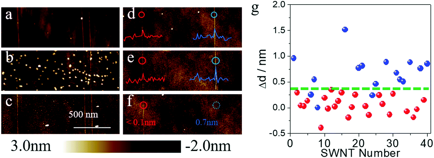 | ||
| Fig. 3 Verifying the effect of adsorbents in the gas-phase etching process. (a–c) In situ AFM image of as-grown SWNTs, and SWNT arrays after being immersed into 5% SDS aqueous solution for 15 min and gas-phase etched for 10 min at 480 °C. (d–f) In situ AFM image of as-grown SWNTs, and SWNT arrays after being immersed into 1% SDS aqueous solution for 12 h and gas-phase etched under the same conditions. (g) Statistics of diameter changes for 40 SWNTs. Red dots refer to the remaining SWNTs, while blue ones refer to the tubes removed after IA gas-phase etching. | ||
A real-time optical observation of the etching process was assisted by the SDS igniter. As shown in Fig. 4b–e, we found that in the first two frames, the carbon nanotube could be observed obviously as a dark line (highlighted with a white arrow). In the third frame, the contrast of the SWNTs significantly decreased and in the fourth frame, the SWNTs could no longer be observed. This phenomenon indicated that the etching process finished rapidly between 1′30′′ and 1′33′′, which is beyond our time-resolution. Our previous work14 analyzed the carbon nanotube etching process in air in detail, and came up with a random etching model to describe this process. Due to a self-terminating behavior, carbon nanotubes show discrete etching on the body of the SWNTs with a gap length depending on the temperature. Corresponding to the etching process of IA gas-phase etching, the gap length of this process should be larger than 50 μm, which possibly happened to be an etching process with the etching temperature higher than 650 °C.
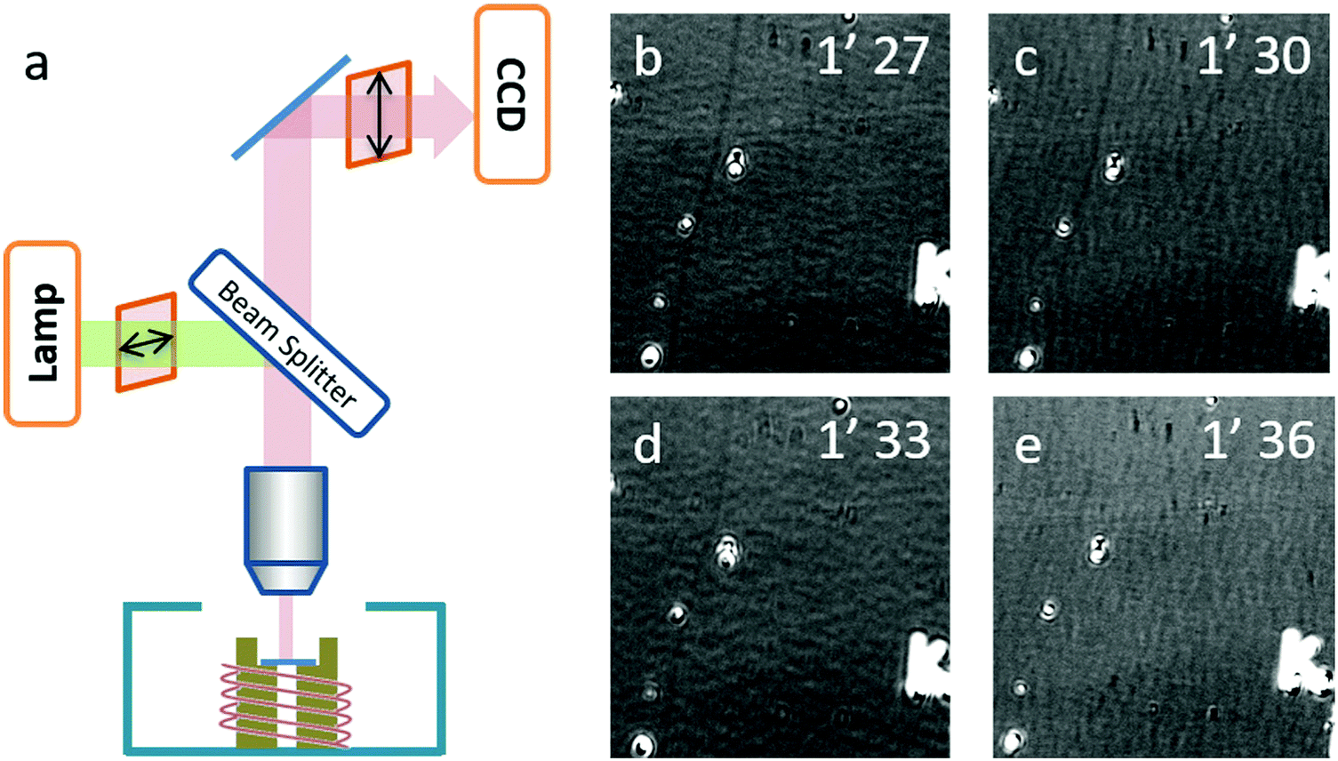 | ||
| Fig. 4 Real-time observation of IA gas-phase etching. (a) Schematic illustration of the polarized optical microscope used for real-time observation. (b–e) Key frames during the IA gas-phase etching process. | ||
According to the above discussion, we proved the importance of SDS in selective gas-phase etching. Besides, as shown in Fig. S3 (ESI†), we also proceeded with a quantitative measurement for analyzing the adsorption capacity. We chose a powder-like SWNT sample synthesized by the arc-discharge method considering that (a) the average diameter of this sample (1.7 nm) is similar to our as-grown samples and (b) the amount of sample was large enough for the test. We used an Energy Dispersive Spectrometer (EDS) to analyze the molecular proportion of carbon and sodium. Pure SDS was used as a standard substance, which showed a peak area ratio of 3.2 (AC![[thin space (1/6-em)]](https://www.rsc.org/images/entities/char_2009.gif) :ANa, A refers to peak area). On the other hand, samples with adsorbents showed a carbon-to-sodium peak area ratio of 53.6. Considering the linear density of carbon atoms on an SWNT with an average diameter of 1.7 nm, the average adsorption capacity on a m-SWNT should be 14.7 molecules per μm (considering that one third SWNTs are metallic ones). Estimated by the heat capacity of graphene and the combustion enthalpy of SDS, if 1% of the energy could be conducted onto the SWNT during the oxidation of SDS, the temperature of the adsorbed SWNTs could be 94 K higher than the non-adsorbed ones. These experiments could provide rationalities to the mechanism of our IA gas-phase etching. Under this etching temperature, pristine SWNTs could not be etched, or were etched with a very low etching rate. However, the temperature is high enough for the adsorbents to be oxided rapidly, and parts of the combustion heat could be conducted to the contacting SWNTs, which makes the actual temperature of the SWNTs much higher than the etching temperature, and they could be etched rapidly. Radicals during the etching process may also decrease the stability of SWNTs in air, but this process is difficult to verify definitely.
:ANa, A refers to peak area). On the other hand, samples with adsorbents showed a carbon-to-sodium peak area ratio of 53.6. Considering the linear density of carbon atoms on an SWNT with an average diameter of 1.7 nm, the average adsorption capacity on a m-SWNT should be 14.7 molecules per μm (considering that one third SWNTs are metallic ones). Estimated by the heat capacity of graphene and the combustion enthalpy of SDS, if 1% of the energy could be conducted onto the SWNT during the oxidation of SDS, the temperature of the adsorbed SWNTs could be 94 K higher than the non-adsorbed ones. These experiments could provide rationalities to the mechanism of our IA gas-phase etching. Under this etching temperature, pristine SWNTs could not be etched, or were etched with a very low etching rate. However, the temperature is high enough for the adsorbents to be oxided rapidly, and parts of the combustion heat could be conducted to the contacting SWNTs, which makes the actual temperature of the SWNTs much higher than the etching temperature, and they could be etched rapidly. Radicals during the etching process may also decrease the stability of SWNTs in air, but this process is difficult to verify definitely.
Besides, we also found that the selectivity in the IA gas-phase etching process is significantly influenced by the heating rate instead of the etching temperature. As shown in Fig. S4 (ESI†), as-grown samples covered by 4HP molecules were heated to 480 °C in air in 20, 10 and 1 min separately. From this we found that samples with a shorter heating time showed a better selectivity after the gas-phase etching process. SWNT arrays heated to 480 °C in 1 min could get an m-SWNT enrichment of 86%, while those heated to the same temperature in 10 min could only get a 54% metallic selectivity. We claimed that this decrease in selectivity is caused by the desorption of 4HP on the SWNTs during the heating process. To verify this, we annealed the SWNT arrays after the absorption process at 300 °C for 10 min in the protection of Ar. Then Raman spectra showed that the metallic selectivity after gas-phase etching significantly decreased to 43%, which was not very different from the raw samples. This phenomenon reflected the importance of adsorbents from the side.
Finally, as our IA gas-phase etching method shows a potential ability in obtaining semiconducting SWNT horizontal arrays, we fabricated back-gated SWNT array FETs using SDS assisted gas-phase etched samples. As shown in Fig. 5a, the samples after the etching process were transferred from an ST-cut quartz substrate to heavily doped silicon substrates (∼300 nm insulating silica layer). An FET device typically contained several nanotubes. Typical I–V curves shown in Fig. 5b reveal semiconducting behavior for the channel materials, that is, the s-SWNTs. The semiconducting tube content of 100 valid devices has been counted, in which over 96% of them showed an on-off ratio higher than 10, which indicates a semiconducting content of more than 90%. The results from electronic devices strongly agree with the results obtained by Raman measurements.
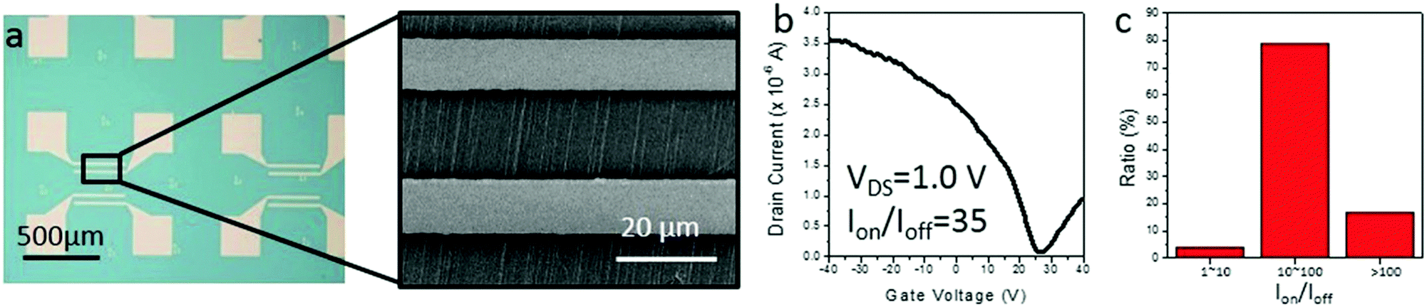 | ||
| Fig. 5 Electrical property characterization of semiconducting enriched SWNT arrays. (a) Optical and SEM images of the FET devices fabricated on the gas-phase etched SWNT arrays covered by SDS transferred onto an SiO2/Si substrate; (b) a typical transfer characteristic curve for the s-SWNT device with Vds = 1 V; (c) the statistical result of the Ion/Ioff ratio of the devices. | ||
Conclusions
In summary, we developed a new method to selectively remove SWNTs with specific electronic types, which is termed as ‘igniter-assisted gas-phase etching’. Under moderate etching conditions, the adsorbents could act as an igniter to accelerate the oxidation of absorbed SWNTs, while the non-adsorbed SWNTs with suitable diameter could remain intact completely. To our best knowledge, this is the first time that SWNTs with different electronic properties have been sorted using one etchant in a gas-phase etching process. Our improved method broke though the limitation of pristine activity of SWNTs during chemical reaction in traditional gas-phase etching processes by introducing the advantages of solution separation (high selectivity and diversity). We believe that this method could bring more possibilities to gas-phase etching, and provide more strategies in obtaining metallic or semiconducting SWNT arrays with high selectivity.Methods
Growth of horizontally aligned SWNTs on the quartz substrate
In particular, ST-cut quartz substrates (single side polished, miscut angle <0.5°, surface roughness <5 Å) were purchased from Hefei Kejing Materials Technology Co., China. After cleaning, the quartz substrates undergo a necessary annealing process (at 900 °C in air for 8 h) for a better crystallization. Catalyst precursor (0.05 mmol, FeCl3 ethanol solution) was dispersed onto the substrate. The SWNT growth was performed in a furnace with a 1 inch tube. The quartz substrates with well-dispersed iron species were put into the tube and heated in air from room temperature to 830 °C in 40 min. Then the system was purged with 300 standard cubic centimeters per minute (sccm) argon for 10 min. After that, 300 sccm H2 was purged for 10 min, and then argon (30 sccm, through an ethanol bubbler) was introduced for the growth of SWNT arrays at 830 °C for 15 min. Then, the sample is cooled down to below 200 °C naturally under the protection of Ar.Preparation of metallic-type molecule igniters
0.5 g SDS (electrophoresis-grade, Sinopharm Chemical Reagent Co., Ltd) was dissolved into 50 mL ultrapure water. As-grown SWNT samples were immersed into the solvent for 12 h under room temperature. After the adsorption process, the sample was carefully moved into ultrapure water and immersed for 5 min for washing off residual SDS. The washing process was repeated 5 times.Preparation of semiconducting-type molecule igniters
0.5 g 4HP was dissolved into 56.4 mL (50 g) toluene (AR, Beijing Tong Guang Fine Chemicals Company). As-grown SWNT samples were immersed into the solvent for 12 h under room temperature. After the adsorption process, the sample was carefully moved into fresh toluene and immersed for 5 minutes for washing off residual 4HP. The washing process was repeated for 5 times.Morphology characterization of SWNTs
A scanning electron microscope (SEM, Hitachi S4800 field emission, Japan, operated at 1.0 kV) and an atomic force microscope (Dimension Icon, Bruker, ScanAsyst mode) were used.Raman scanning of SWNTs
The SWNTs on quartz were transferred from quartz to a SiO2/Si substrate with a 300 nm oxide layer by using the previously reported polymer-assisted method.1 A Raman spectroscope (WITec, alpha 300) was used for the characterization of the SWNTs. The wavelengths of the excitation lasers for Raman spectroscopy were 488 and 633 nm. The line scanning interval was 1 micron, which matched the diameter of the laser plot (∼1 micron with a 100× objective lens).Real-time observation of the etching process
An optical microscope (Olympus BX51) equipped with a 50× objective (N.A. = 0.5, working distance of 1.06 cm), two polarizers (Daheng optics, GCL-050003) and a monochrome camera (Andor Zyla 4.2) were used to image the carbon-nanotube in situ. A tungsten–halogen lamp was used as the light source, the reflective mode was used, one polarizer was located in the incident beam with its transmission axis set horizontally, and the second polarizer was placed in the reflective beam with its transmission axis set to a small angle θ from the vertical direction. The as-grown SWNT substrates were placed into a hot-wall reactor exposed to atmospheric phenomena. The samples were heated up to the target temperature at 100 °C per minute. The etching process was monitored by real-time video mode.Sample preparation for EDS analysis
0.05 g powder-like SWNTs synthesized by the arc-discharge method were added into 200 mL 1% SDS aqueous solution, and then the mixture was treated in a cup-horn sonicator at a power level of 300 W for 2 h. Immediately after sonication, samples were centrifuged at 20000 rpm for 1 h. About 40% of the supernatant liquid was carefully collected. Then, vacuum filtration was carried out and the SWNT film was washed by ultrapure water 3 times. Then the film was re-dispersed into water treated by a cup-horn sonicator at a power level of 300 W for 2 h. The solution was then dispensed onto a SiO2/Si substrate with a 300 nm oxide layer for further analysis.
Fabrication and measurements of electrical devices
The SWNTs on quartz were transferred from quartz to a SiO2/Si substrate with a 300 nm oxide layer by using the previously reported polymer-assisted method. Electrodes were patterned by photolithography with a channel length of 20 μm. Cr (3–5 nm)/Au (50 nm) were deposited by thermal evaporation. The electrical measurement was performed using a Keithley 4200-SCS semiconductor characterization system.Conflicts of interest
There are no conflicts to declare.Acknowledgements
This work was supported by the Ministry of Science and Technology of China (2016YFA0200101 and 2016YFA0200104), the National Natural Science Foundation of China (grant No. 21233001, 21790052 and 51720105003) and the Beijing Municipal Science and Technology Planning Project (No. Z161100002116026).Notes and references
- C. Liu and H. M. Cheng, J. Am. Chem. Soc., 2016, 138, 6690 CrossRef CAS PubMed.
- S. C. Zhang, L. X. Kang, X. Wang, L. M. Tong, L. W. Yang, Z. Q. Wang, K. Qi, S. B. Deng, Q. W. Li, X. D. Bai, F. Ding and J. Zhang, Nature, 2017, 543, 234 CrossRef CAS PubMed.
- (a) H. Guo, M. Zhou, Z. Ruoxing, H. Shimin, C. Wonmook, W. Yun Sung, C. Jae-Young, L. Zhongfan and Z. Jin, Angew. Chem., Int. Ed., 2011, 50, 6819 CrossRef PubMed; (b) B. Yu, P. X. Hou, F. Li, B. L. Liu, C. Liu and H. M. Cheng, Carbon, 2010, 48, 2941 CrossRef CAS; (c) H. L. Zhang, Y. Q. Liu, L. C. Cao, D. C. Wei, Y. Wang, H. Kajiura, Y. M. Li, K. Noda, G. F. Luo, L. Wang, J. Zhou, J. Lu and Z. X. Gao, Adv. Mater., 2009, 21, 813 CrossRef CAS; (d) T. Tanaka, H. Jin, Y. Miyata, S. Fujii, H. Suga, Y. Naitoh, T. Minari, T. Miyadera, K. Tsukagoshi and H. Kataura, Nano Lett., 2009, 9, 1497 CrossRef CAS PubMed; (e) G. Zhang, P. Qi, X. Wang, Y. Lu, X. Li, R. Tu, S. Bangsaruntip, D. Mann, L. Zhang and H. Dai, Science, 2006, 314, 974 CrossRef CAS PubMed.
- D. Tasis, N. Tagmatarchis, A. Bianco and M. Prato, Chem. Rev., 2006, 106, 1105 CrossRef CAS PubMed.
- A. Li-Pook-Than, J. Lefebvre and P. Finnie, ACS Nano, 2013, 7, 6507 CrossRef CAS PubMed.
- J. G. Wiltshire, A. N. Khlobystov, L. J. Li, S. G. Lyapin, G. A. D. Briggs and R. J. Nicholas, Chem. Phys. Lett., 2004, 386, 239 CrossRef CAS.
- (a) S. Nagasawa, M. Yudasaka, K. Hirahara, T. Ichihashi and S. Iijima, Chem. Phys. Lett., 2000, 328, 374 CrossRef CAS; (b) B. Yu, C. Liu, P. X. Hou, Y. Tian, S. S. Li, B. L. Liu, F. Li, E. I. Kauppinen and H. M. Cheng, J. Am. Chem. Soc., 2011, 133, 5232 CrossRef CAS PubMed.
- J. M. Simmons, B. M. Nichols, S. E. Baker, M. S. Marcus, O. M. Castellini, C. S. Lee, R. J. Hamers and M. A. Eriksson, J. Phys. Chem. B, 2006, 110, 7113 CrossRef CAS PubMed.
- (a) A. Hassanien, M. Tokumoto, P. Umek, D. Vrbanic, M. Mozetic, D. Mihailovic, P. Venturini and S. Pejovnik, Nanotechnology, 2005, 16, 278 CrossRef CAS PubMed; (b) P. X. Hou, W. S. Li, S. Y. Zhao, G. X. Li, C. Shi, C. Liu and H. M. Cheng, ACS Nano, 2014, 8, 7156 CrossRef CAS PubMed.
- (a) W. Zhou, S. Zhan, L. Ding and J. Liu, J. Am. Chem. Soc., 2012, 134, 14019 CrossRef CAS PubMed; (b) J. Li, K. Liu, S. Liang, W. Zhou, M. Pierce, F. Wang, L. Peng and J. Liu, ACS Nano, 2014, 8, 554 CrossRef CAS PubMed; (c) P. Li and J. Zhang, J. Mater. Chem., 2011, 21, 11815 RSC.
- J. Lu, S. Nagase, X. W. Zhang, D. Wang, M. Ni, Y. Maeda, T. Wakahara, T. Nakahodo, T. Tsuchiya, T. Akasaka, Z. X. Gao, D. P. Yu, H. Q. Ye, W. N. Mei and Y. S. Zhou, J. Am. Chem. Soc., 2006, 128, 5114 CrossRef CAS PubMed.
- (a) M. S. Arnold, A. A. Green, J. F. Hulvat, S. I. Stupp and M. C. Hersam, Nat. Nanotechnol., 2006, 1, 60 CrossRef CAS PubMed; (b) D. Liu, P. Li, X. Q. Yu, J. T. Gu, J. Han, S. C. Zhang, H. B. Li, H. H. Jin, S. Qiu, Q. W. Li and J. Zhang, Adv. Mater., 2017, 29, 1603565 CrossRef PubMed.
- (a) H. P. Liu, D. Nishide, T. Tanaka and H. Kataura, Nat. Commun., 2011, 2, 309 CrossRef PubMed; (b) Y. Hu, Y. B. Chen, P. Li and J. Zhang, Small, 2013, 9, 1306 CrossRef CAS PubMed; (c) J. Han, Q. Y. Ji, H. B. Li, G. Li, S. Qiu, Q. C. Zhang, H. H. Jin, Q. W. Li and J. Zhang, Chem. Commun., 2016, 52, 7683 RSC.
- Q. Zhao, F. Yao, Z. Wang, S. Deng, L. Tong, K. Liu and J. Zhang, Adv. Mat., 2017, 1701959 CrossRef PubMed.
Footnote |
| † Electronic supplementary information (ESI) available: Stability of non-adsorbed SWNTs under etching condition; Quantitative analysis of the SDS adsorbing capacity on SWNTs; Etching selectivity assisted by 4HP with different heating process. See DOI: 10.1039/c7qm00469a |
| This journal is © the Partner Organisations 2018 |