
Recent progress in interface engineering of organic thin film transistors with self-assembled monolayers†
Danqing
Liu
 *a and
Qian
Miao
*b
*a and
Qian
Miao
*b
aShenzhen Key Laboratory of Polymer Science and Technology, College of Materials Science and Engineering, Shenzhen University, Shenzhen, 518060, China. E-mail: dqliu@szu.edu.cn
bDepartment of Chemistry, the Chinese University of Hong Kong, Shatin, New Territories, Hong Kong, China. E-mail: miaoqian@cuhk.edu.hk
First published on 31st August 2017
Abstract
Organic thin film transistors (OTFTs) are basically interface devices with their performance being strongly dependent on the structures and properties of the device interfaces. Self-assembled monolayers (SAMs) have been developed as a powerful platform for interface engineering of OTFTs. This review provides an introduction to the structures of OTFTs as well as the structures and characterizations of SAMs, and focuses on the recent progress in interface engineering of OTFTs with SAMs. On the basis of the discussion on recent progress, we finally reach conclusions on the current status of research on interface engineering of OTFTs with SAMs and provide an outlook for the development of this molecular platform in the near future.
 Danqing Liu | Dr Danqing Liu graduated from the University of Science and Technology of China with a BSc degree in 2010. She earned her PhD degree from the Chinese University of Hong Kong in 2014, and joined Shenzhen University as an Assistant Professor in 2015. Her current research focuses on organic electronic devices, including molecular materials, self-assembly, and solution processing. |
 Qian Miao | Prof. Qian Miao graduated from the University of Science and Technology of China with a BSc degree in 2000. He received his PhD degree from Columbia University in 2005 under the direction of Prof. Colin Nuckolls, and then did postdoctoral research with Prof. Fred Wudl in the University of California, Los Angeles. He joined the Chinese University of Hong Kong as an assistant professor in 2006, and was promoted to Associate Professor in 2012 as well as Professor in 2016. His research group investigates novel polycyclic aromatics and high-performance organic electronic materials on the basis of organic chemistry and by using tools from organic synthesis, supramolecular chemistry and surface chemistry. |
Introduction
An organic thin film transistor (OTFT) is a type of elemental device for organic semiconductors, which, unlike conventional inorganic semiconductors, are mechanically flexible, compatible with inexpensive solution-based fabrication over large areas and capable of various functionalities through molecular design and organic synthesis. With these advantages, light-weight, flexible and low-cost organic electronic devices are of great fundamental interest in materials science and are also recognized as a growing market for industry. Organic integrated circuits that are composed of OTFTs as elemental units are applied, for example, to operate radio-frequency identification (RFID) tags and sensors and to drive individual pixels in light-weight and flexible displays.1,2 OTFTs are basically interface devices with their performance strongly relying on the structures and properties of the device interfaces. Therefore, tailoring interface structures and properties is as important as developing new semiconductor materials for the ultimate success of OTFTs. A variety of strategies have been developed for interface engineering of OTFTs3,4 by modifying the interfaces with different chemical species, such as self-assembled monolayers (SAMs), polymers,5,6 non-covalently bonded small molecules,7,8 metal oxides9 and graphene oxide.10 SAMs are two-dimensional molecular assemblies of organic molecules forming spontaneously on a variety of surfaces by chemisorption, which involves a chemical reaction between the surface and the adsorbed molecules.11 A SAM is only a few nanometers thick but can dramatically manipulate the surface properties. In virtue of this unique capability, SAMs have been developed as a powerful molecular platform for interface engineering of OTFTs, which has already been reviewed in the literature.3,4,12–15 In order to avoid overlap with these published reviews, in this review we emphasize the most recent progress in interface engineering of OTFTs with SAMs after an introduction to the structures of OTFTs as well as the structures and characterizations of SAMs. On the basis of this discussion, we finally reach conclusions on the current status of research on interface engineering of OTFTs with SAMs and provide an outlook for the development of this molecular platform in the near future.Structures of OTFTs
An OTFT typically consists of a thin film of organic semiconductors, three electrodes (gate, drain and source) and a dielectric layer between the semiconductor and the gate electrode. Depending on whether the gate is placed below or above the semiconductor, OTFTs are classified as bottom- or top-gate devices, respectively; and depending on whether the drain and source electrodes are placed below or above the semiconductor, OTFTs are classified as bottom- or top-contact devices respectively. OTFTs essentially act as an on/off switch, where the electrical current between the drain and source electrodes (IDS) depends on not only the voltage between the drain and source electrodes (VDS) but also the voltage between the gate and source electrodes (VGS). The most important parameter to characterize the performance of OTFTs is the field effect mobility (μFET), which characterizes how fast a charge carrier (a hole or an electron) can move through the organic semiconductors under an applied electric field. Higher field effect mobility allows OTFTs to be used for wider applications. Two important interfaces in OTFTs that determine device performances are: (1) the interface between organic semiconductors and gate dielectrics, where the first few molecular layers of organic semiconductors are the locus of charge transport and responsible for current modulation16 and (2) the interface between semiconductors and metal electrodes, where charge injection occurs from the metal into the semiconductors. Fig. 1 shows an OTFT with a bottom-gate and bottom-contact configuration highlighting the above two interfaces. Moreover, the interface between semiconductors and the environment becomes important when OTFTs are designed to function as sensors, where the adsorption of analyte molecules leads to a change in the channel conductivity. In contrast, for other applications of OTFTs, the semiconductor surface can be sealed with a passive layer (such as a stable polymer) to isolate the device from any environmental influences and damage.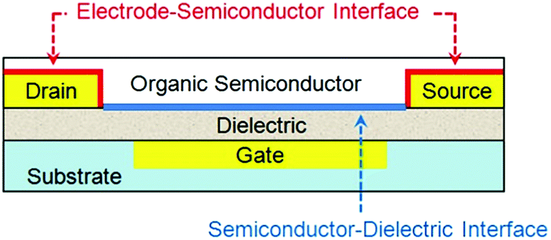 | ||
| Fig. 1 Schematic structure of a bottom-contact bottom-gate OTFT highlighting the two device interfaces. | ||
Most OTFTs are bottom-gate devices, which have organic semiconductors directly deposited onto the dielectric surface. Therefore the dielectric surface has large impacts on the performance of OTFTs in two aspects. First, during fabrication of semiconductor films, the properties of the dielectric surface, such as surface energy and surface roughness, largely determine the structures of organic semiconductor films in terms of molecular ordering,17 molecular orientation and film morphology. Second, the properties of the dielectric surface, such as surface dipole and trap states, greatly affect the accumulation and transport of charge carriers in organic semiconductors at the interface.18
The metal–semiconductor interface is formed by the deposition of metal electrodes typically through a shadow mask on pre-formed organic films in top-contact OTFTs or by the deposition of organic films on pre-patterned metal electrodes in bottom-contact OTFTs. For efficient charge injection into organic semiconductors, the work function of the electrode has to match the highest occupied molecular orbital (HOMO) energy level of p-type semiconductors or the lowest unoccupied molecular orbital (LUMO) energy level of n-type semiconductors.19 Otherwise a potential barrier is formed, leading to poor charge injection and high contact resistance. Another problem related to the metal–semiconductor interface is that the bottom-contact OTFTs usually exhibit poorer performance than the top-contact OTFTs, where the top-contact source/drain electrodes unfortunately are not compatible with photolithographic patterning in low-cost fabrication. The inferior performance of the bottom-contact OTFTs, including greater contact resistance and lower charge carrier mobility, can be mainly attributed to the interface between the metal electrode and the dielectric oxide, which is not present in the top-contact OTFTs. The growth of semiconductor films over the interface between the dielectric oxide and the metal electrode usually results in a discontinuous morphology, and the semiconductor grain structures that form on the dielectric oxide surface and on the metal electrode surface are usually different.20
Structures and characterization of SAMs
SAMs provide a convenient and flexible simple system to tailor the interfacial properties of metals and dielectric oxides owing to their unique structures. As shown in Fig. 2, molecules that form SAMs comprise three parts: an anchor group (also known as the head group), a terminal group and a linker.21,22 A typical structure for such a molecule is an α,ω-functionalized alkane, which has a head (α) group and a terminal (ω) group linked together with an alkyl chain. An overly simple rule often used to design new SAMs is that an α,ω-functionalized alkane will form ordered SAMs with the head group anchored onto the substrate and the terminal group present at the exposed surface.21 An obvious problem with this rule is that it neglects the influences of the volume and interactions of terminal groups. It assumes that the organization, conformation and orientation of α,ω-functionalized alkanes with small terminal functional groups, such as –CH3, –OH and –CN, also apply to other SAMs. The guidelines that can incorporate the influences of terminal groups to predict molecular assemblies in the monolayer are yet to be developed.21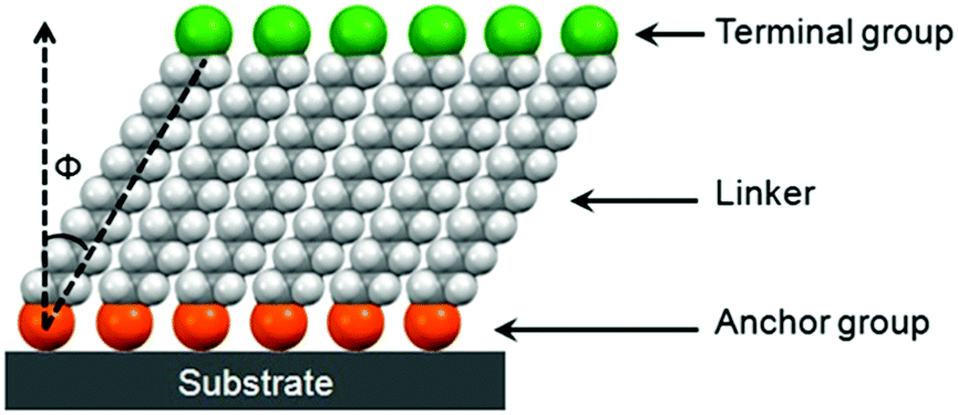 | ||
| Fig. 2 Schematic diagram of a SAM. | ||
The head groups of SAM molecules have a specific affinity for a substrate with respect to the selective formation of chemical bonds with surface atoms of the substrate. The most widely investigated SAMs for interface engineering of OTFTs are thiolates on gold, silanes on SiO2 and phosphonic acids on metal oxides. The SAMs of thiolates on gold are commonly formed by the treatment of gold with thiols or disulfides, which react with the surface metal atoms forming relatively weak Au–S bonds with a homolytic bond strength on the order of ca. 50 kcal mol−1.11 Both silanes and phosphonic acids require hydroxylated surfaces as substrates to form SAMs; nevertheless their formation mechanisms are different. The formation of organosilane SAMs typically involves hydrolysis of RSiX3 (X![[double bond, length as m-dash]](https://www.rsc.org/images/entities/char_e001.gif) Cl or OCH3) by water molecules that are already adsorbed on the oxide surface, to create the corresponding hydroxysilane, and the subsequent condensation reaction, which occurs between the Si–OH groups to form Si–O–Si bonds, not only with the surface –OH groups but also with the neighbouring silanol groups. In this way, silane molecules are not all individually linked to the surface, but rather form a cross-linked network that also contains many covalent bonds with the underlying surface.23 The SAMs of phosphonic acids are anchored onto metal oxides with strong covalent P–O–M bonds, which are formed by the heterocondensation reaction of phosphonic acids with surface hydroxyl groups. The presence of three oxygen atoms on the phosphonates allows mono-, bi-, and tri-dentate binding modes in combination with possible electrostatic and hydrogen-bonding interactions depending on the nature of the oxide substrate as well as the reaction conditions.23
Cl or OCH3) by water molecules that are already adsorbed on the oxide surface, to create the corresponding hydroxysilane, and the subsequent condensation reaction, which occurs between the Si–OH groups to form Si–O–Si bonds, not only with the surface –OH groups but also with the neighbouring silanol groups. In this way, silane molecules are not all individually linked to the surface, but rather form a cross-linked network that also contains many covalent bonds with the underlying surface.23 The SAMs of phosphonic acids are anchored onto metal oxides with strong covalent P–O–M bonds, which are formed by the heterocondensation reaction of phosphonic acids with surface hydroxyl groups. The presence of three oxygen atoms on the phosphonates allows mono-, bi-, and tri-dentate binding modes in combination with possible electrostatic and hydrogen-bonding interactions depending on the nature of the oxide substrate as well as the reaction conditions.23
The alkyl chains of SAM molecules play a critical role in the formation of ordered supramolecular structures through inter-chain van der Waals interactions, which become stronger as the alkyl chain length increases. As shown in Fig. 2, the alkyl chains in SAMs usually have a tilt (Φ) from the surface normal, which varies with different SAM molecules and substrates as well as the phase of SAMs. As found from the SAMs of alkyl phosphonic acids on metal oxides and alkyl thiols on gold, as the alkyl chain length increases, the SAM ordering increases and the molecular tilt angle decreases.24,25 For a specific SAM molecule on a certain substrate, usually a smaller tilt angle is indicative of a higher packing density in a more “ordered” or “solid-like” state, while a larger tilt angle indicates a lower packing density accompanying a “disordered” or “liquid-like” state.22 The terminal group, also known as the surface group or tail group, determines the surface properties depending on its chemical structure.
The structures and properties of SAMs are usually characterized in terms of chemical composition, monolayer thickness and packing density, molecular ordering and crystallinity, wetting behaviour and dipole. Characterization of such a one-molecule-thick nanostructure is often a challenging task requiring high sensitivity and combination of different techniques. Spectroscopic ellipsometry is a widely used technique to measure the thickness of SAMs based on the change in the polarization of light upon reflection by the SAMs.26 X-ray based techniques, including X-ray photoelectron spectroscopy (XPS),27,28 X-ray reflectivity (XRR),29 near-edge X-ray absorption fine structure spectroscopy (NEXAFS), and grazing incidence X-ray diffraction (GIXD), are powerful tools to study the structures of SAMs. XPS is a surface-sensitive technique that measures the kinetic energy and number of electrons escaping from the material surface upon irradiation with X-ray beams. It can be used to qualitatively determine the composition and oxidation state of elements, and to semi-quantitatively evaluate atomic percentage. The ratio of the integrated peak areas for the Si(2p) and C(1s) XPS signals was used as a measure of the relative chain packing density of the alkyl silane SAMs on a SiO2 substrate.30 By measuring the specular reflection of X-rays from the sample surface, XRR is a surface-sensitive technique for absolute measurement of the thickness, density and roughness of SAMs.31,32 However XRR relies on complicated model fitting. NEXAFS measures electronic transitions near the absorption edge of an atom commonly with high intensity, monochromatic, linearly polarized X-rays from a synchrotron source.24 Analyses of the electronic transitions near the carbon K-edge are commonly used to characterize molecular ordering of long-chain alkyl groups in SAMs.33,34 The chain tilt angle can also be calculated from the spectra according to the Outka and Stohr's method.35,36 By exposing thin films to high intensity synchrotron X-rays under a very small angle (∼0.1°), GIXD allows the X-rays to penetrate and to be scattered not only out-of-plane (perpendicular to the substrate) but also in-plane. With in-plane diffraction, GIXD is a very useful tool to study the two-dimensional (2D) crystal structure of SAMs. Scanning tunnelling microscopy (STM) can also provide a direct image for the 2D structure of SAMs, but it is only applicable to highly crystalline and ultra smooth SAMs on conductive substrates. Fourier transform infrared spectroscopy (FT-IR) is a convenient technique for the evaluation of monolayer packing density by comparing the integrated areas of the concerned absorption bands.37 Because the packing density is usually correlated with the molecular ordering of alkyl chains in a specific SAM on the same substrates, FT-IR is also useful for the evaluation of the molecular ordering of SAMs. The wettability of SAMs can be evaluated by measuring the contact angle of a liquid drop.38 The contact angle commonly depends on the free energies of the liquid and the surface. High-energy surfaces can be easily wetted by most liquids with a small contact angle; while low-energy surfaces are difficultly wetted by liquids with a contact angle greater than 90°.39,40 The surface free energy comprising a dispersive component and a polar component can be determined by measuring the contact angles of the two probe liquids, for example, water and diiodomethane.38,41 In addition, atomic force microscopy (AFM) is widely used to evaluate the smoothness of SAMs. More details on various characterization techniques can be found in the published reviews.22,42
Engineering of semiconductor–dielectric interfaces with SAMs
Modification of the dielectric surface with SAMs can manipulate the structures and properties of dielectric surfaces in terms of surface roughness, surface energy, surface dipole, and lattice structures, and improve charge transport at the semiconductor–dielectric interface.12,18,43 The SAMs play important roles both in the formation of semiconductor films during device fabrication and in the accumulation and transport of charge carriers in organic semiconductors during device operation. The nano-structures of SAMs can be changed by chemically modifying the anchor group, the terminal group and the linker in the SAM-forming molecule or by varying the conditions for adsorption and reaction of the molecules on the surface. For modification of the dielectric oxide surface, the SAM-forming molecules usually have trichlorosilane, trimethoxysilane or phosphonic acid as the anchor group. Because the available anchor groups are very limited, studies on the effects of anchor groups are rare. Bao and co-workers compared the SAMs of octadecylphosphonic acid (C18-PA in Fig. 3) and octadecyltrichlorosilane (ODTS in Fig. 3), which have the same octadecyl chains but different anchor groups, namely, phosphonic acid and trichlorosilane, respectively.31 It was found that the electric dipoles in the gate dielectric could be manipulated with different anchor groups and the different dipoles between the C18-PA and ODTS SAMs resulted in significant voltage shifts in the current–voltage curves of the OTFTs. The SAM of C18-PA, through the effects of dipoles, suppresses the trapping of electrons due to air exposure and greatly enhanced the air stability of n-channel OTFTs based on C60 and N,N′-ditridecyl-3,4,9,10-perylenetetracarboxylic diimide (PTCDI-C13 as in Fig. 4). In the following sections, recent studies on SAM-modified dielectric surfaces are organized according to the methods used to change the SAM structures. | ||
| Fig. 3 Representative structures of molecules that form SAMs on dielectric oxides for interface engineering of OTFTs. | ||
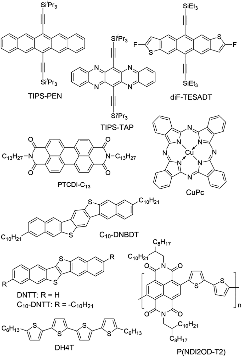 | ||
| Fig. 4 Selected structures of organic semiconductors as mentioned. | ||
Tailoring terminal groups
The surface properties of SAMs, such as the surface energy and surface dipole, can be conveniently tailored by changing the terminal groups. The initial nucleation behaviour of organic semiconductor molecules is strongly influenced by the surface energy of the substrate when the organic semiconductor films are deposited by vacuum deposition. A higher surface energy prefers a layer-by-layer growth mode (also known as Frank–van der Merwe growth) due to stronger substrate–film interactions; while a lower surface energy prefers an island growth mode (also known as Volmer–Weber growth) because of stronger intermolecular interactions. As an intermediary process characterized by both two-dimensional (2D) layer and three-dimensional (3D) island growth, layer-plus-island growth (also known as Stranski–Krastanov growth) is commonly observed in the formation of organic semiconductor films by vacuum deposition.44 3D nucleation is usually undesirable for OTFTs, because it generates rough, non-uniform films with severe grain boundaries, which act as trap sites greatly impeding transport of charge carriers. In contrast, the layer-by-layer mode of growth is desired for transistor applications because it leads to large, well-connected domains that facilitate charge transport parallel to the substrate.To investigate the impact of energetically engineered dielectrics, Lee et al. compared the SAMs of 1H,1H,2H,2H-perfluorodecyltrichlorosilane (FTS), (3-aminopropyl)trimethoxysilane (APS), phenyltrichlorosilane (PTS) and hexamethyldisilazane (HMDS), which have fluoro, amino, phenyl, and methyl terminal groups, respectively, as shown in Fig. 3.45 The surface energy of FTS, APS, PTS and HMDS SAMs was measured as 0.0186, 0.0514, 0.0452, and 0.0318 N m−1, respectively. Vacuum-deposition of 6,13-bis((triisopropylsilyl)ethynyl)pentacene (TIPS-PEN in Fig. 4) on the SAM of PTS led to layer-plus-island growth providing semiconductor films with the best morphological and crystalline structures. This was attributed to the strong intermolecular π–π interactions between TIPS-pentacene and the SAM of PTS as well as the matched surface energies. Pujari et al. also reported that the surface energies of copper(II) phthalocyanine (CuPc in Fig. 4), SiO2, ODTS-modified SiO2, and phenylhexyltrichlorosilane (PHTS)-modified SiO2 are 0.0351, 0.0685, 0.0329, and 0.0385 N m−1, respectively.46 The observed higher mobility of the CuPc thin film with a more 2D growth mode at the PHTS-modified dielectric interface is suggested as a result of matching the surface energy of the dielectric and organic semiconductors.
Surface energy is also of key importance to the growth of organic semiconductor films during a solution-based process because the nucleation and growth of semiconductor molecules during solution-based processing depends on the wetting behaviour of the semiconductor solution on the dielectric surface. Tsurumi et al. reported solution-processed single-crystalline OTFTs based on two p-type semiconductors, C10-DNBDT and C10-DNTT (Fig. 4), with the AlOx dielectric modified with a variety of SAMs.47 It was found that the films of C10-DNTT on bare AlOx and the films of C10-DNBDT on the SAMs of 16-phosphonohexadecanoic acid (PHDA in Fig. 3) exhibited the highest mobility (4.3 ± 1.3 cm2 V−1 s−1 and 3.7 ± 0.2 cm2 V−1 s−1, respectively). With surface hydroxyl groups, the bare AlOx and the PHDA SAM have the highest surface energies (0.052 and 0.053 N m−1, respectively) among the surfaces tested in this study. However, hydroxylated surfaces are not suitable for the fabrication of n-channel OTFTs because the surface hydroxyl groups can trap mobile electrons.5
To solve this problem, Miao et al. designed a high-surface-energy SAM by inserting polar oxygen atoms into the long alkyl chain of phosphonic acids.48 With the methoxyl terminal group, the SAM of 12-methoxydodecylphosphonic acid (MODPA in Fig. 3) avoids electron trapping by surface hydroxyl groups and exhibits a surface energy of 0.0430 N m−1, which is higher than that of the C18-PA SAM (0.0266 N m−1). Drop casting solutions of 6,13-bis((triisopropylsilyl)ethynyl)-5,7,12,14-tetraazapentacene (TIPS-TAP in Fig. 4) on the MODPA-modified AlOy/TiOx resulted in high-quality films containing aligned crystalline fibres, leading to solution-processed n-channel OTFTs with a high field effect mobility of up to 2.5 cm2 V−1 s−1. One problem associated with the insertion of oxygen atoms into the long alkyl chains of SAMs is poor air stability for n-channel OTFTs because the oxygen atoms can accumulate water molecules at the semiconductor–dielectric interface by hydrogen bonding. To solve this problem, Miao et al. introduced an unprecedented cyclohexyl terminal group to the SAMs by designing and synthesizing 12-cyclohexyldodecylphosphonic acid (CDPA in Fig. 3).49 The self-assembly of CDPA on the top of AlOy/TiOx resulted in an ordered SAM with a 2D crystal lattice constant of 4.45 Å, which is slightly larger than that of the methyl-terminated SAM of C18-PA (4.2 Å).31 The SAM of CDPA exhibited a higher surface energy (0.0316 N m−1) than that of C18-PA (0.0266 N m−1) on the same oxides likely because a cyclohexyl terminal group has a larger area of contact for van der Waals interactions than a methyl terminal group. With the enhanced surface energy, the CDPA-modified AlOy/TiOx is completely wettable by a variety of organic solvents. The CDPA-modified AlOy/TiOx is found to be generally applicable to solution-processed and vacuum-deposited p- and n-channel OTFTs with high field effect mobility and good air stability. Solution processed OTFTs of TIPS-PEN and TIPS-TAP exhibited an average hole mobility of 1.64 cm2 V−1 s−1 and an average electron mobility of 2.57 cm2 V−1 s−1, respectively. With reduced defects in the dielectric oxides, the solution processed OTFTs of TIPS-TAP on the CDPA-modified AlOx/SiO2 achieved electron mobility as high as 11 cm2 V−1 s−1.50 Furthermore, when two types of SAMs with different terminal groups are used, the dielectric surface can be patterned into wettable and unwettable regions, which allow surface selective deposition of organic semiconductors from solutions.51 Selective growth of organic crystals is facilitated only on the wettable regions, resulting in spontaneous patterning of organic films.52,53
Polar terminal groups in a SAM give rise to surface dipoles, which provide an electric field in addition to the applied gate bias. The additional field is able to control charge carrier density at the semiconductor–dielectric interface. As a result, polar terminal groups on the SAM-modified dielectric surface have shown great influences on the threshold voltage and turn-on voltage of OTFTs.54–56 Iwasa and co-workers showed that SAMs with fluorinated alkyl and amino terminals accumulated holes and electrons, respectively, in the transistor channel.57 Such an effect of the fluorinated alkyl group can be understood in terms of electric dipoles, while the effect of the amino group has been attributed to weak charge transfer between organic films and SAMs. On the basis of the same concept, Würthner et al. demonstrated that the charge transport characteristics of dicyanated isoindigo derivatives in OTFTs could be tuned by the SAMs on the dielectric.58 The SAM of pentadecafluorooctadecylphosphonic acid (F15C18-PA in Fig. 3) gave rise to ambipolar charge transport, while the SAM of n-tetradecylphosphonic acid (C14-PA in Fig. 3) led to unipolar transport of electrons. Similarly, Nakano et al. reported that major charge carriers in an ambipolar polymer semiconductor can be controlled by SAMs with dimethylamino and fluorinated alkyl terminal groups.59 The SAM of 1H,1H,2H,2H-perfluorodecyltriethoxysilane (FDTS in Fig. 3) completely suppressed electron transport giving rise to unipolar p-channel characteristics, whereas the SAM of [3-(N,N′-dimethylamino)propyl]triethoxysilane (MAPS in Fig. 3) completely suppressed hole transport giving rise to unipolar n-channel characteristics. A surface dipole-induced shift of the threshold voltage is often observed in combination with a change in mobility,56,60 which, however, lacks a causal link with the surface dipole. Recent studies have attributed the change of mobility to different film morphologies, which arise from the change in the surface energy as another effect of terminal groups.61,62
Terminal groups of SAMs can also manipulate molecular orientation of organic semiconductors on the dielectric surface. Cho and co-workers reported that the molecules of poly(3-hexylthiophene) had an edge-on orientation on the amino-terminated SAM and a face-on orientation on the methyl-terminated SAM.63 This phenomenon was attributed to the following factors: the lone pair of electrons in the terminal amino groups, the π–H interactions between the π-backbone and the H atoms of the terminal groups, and interdigitation between the alkyl chains of P3HT and the alkyl chains of the SAMs. Halik et al. compared vacuum-deposited films of dihexylquaterthiophene (DH4T in Fig. 4) with three different SAMs of n-decylphosphonic acid (C10-PA in Fig. 3), PHDA, and F15C18-PA.64 On the basis of this study, they concluded that SAMs with high surface energy tended to induce a face-on orientation of the semiconductor molecules, which is favourable for charge transport in OTFTs, whereas SAMs with low surface energy favoured an edge-on orientation. Because surface energy can influence both the film growth mode and the molecular orientation of organic semiconductors, the impact of the surface energy on the device performance of OTFTs is complicated.
Tuning alkyl linkers
The length of the alkyl linker in the SAM-forming molecules is an important factor for determining the molecular ordering of SAMs.24 A longer alkyl chain usually leads to stronger van der Waals interactions and results in a more ordered self-assembly with denser molecular packing.65 Jen et al. systematically investigated SAMs of n-alkyl phosphonic acids on ultra thin (ca. 8 nm) HfO2, and found that the molecular ordering of the SAMs increased from disordered to ordered as the number of carbon atoms in the alkyl chain increased from 6 to 18.66 It was found that the disordered SAMs could promote large pentacene grains. This phenomenon was explained with a proposal that the disordered SAM provides an amorphous liquid-like surface allowing greater pentacene diffusion length and lower nucleation density. As a result, the highest field-effect mobility of pentacene was achieved with the SAM of n-octylphosphonic acid (C8-PA in Fig. 3) with a balance between disordered SAMs to promote large pentacene grains and a SAM thick enough to act as a physical buffer to mitigate the adverse effects of the underlying high-k surface. In close relation to this study, Jen et al. used n-alkyl phosphonic acids to simultaneously modify the bottom-contact silver electrodes and HfO2 dielectric surfaces in OTFTs of pentacene and C60.27 The vacuum-deposited films of pentacene on the SAMs of C8-PA, n-dodecylphosphonic acid (C12-PA in Fig. 3) and C18-PA exhibited average field effect mobilities of 0.60, 0.66 and 0.13 cm2 V−1 s−1 for holes, respectively; and the films of C60 on the SAMs of C8-PA, C12-PA and C18-PA exhibited average field effect mobilities of 3.7, 1.5 and 5 × 10⁻⁴ cm2 V−1 s−1 for electrons, respectively. The higher mobility of pentacene on C8-PA and C12-PA was similarly attributed to the larger grain size as a result of a more amorphous and homogeneous surface providing greater diffusion distance for pentacene molecules. Whereas, the higher mobility of C60 on C8-PA was attributed to the compact morphology of C60 thin films on C8-PA likely as a result of a smaller diffusion length for C60, which, in comparison with pentacene, has stronger intermolecular cohesive forces accompanying island growth in the films. From their study on phenyl-terminated SAMs in OTFTs of pentacene, the same research group reached very similar conclusions on the effect of surface homogeneity on film morphologies and indicated that the surface energy tends to be a negligible factor in device performance provided that surface homogeneity was achieved.33 The surface homogeneity of SAMs being dependent on the alkyl chain length is also supported by molecular dynamics simulations as reported by Halik et al.67 The calculated SAM morphology changes with increasing chain length from an amorphous state for C6-PA (Fig. 3) to a more ordered state for C10-PA (Fig. 3) to highly ordered (crystalline) domains separated by gaps for C14-PA (Fig. 3) and C18-PA. It is proposed that the self-assembly of phosphonic acids with shorter alkyl chains is dominated by the footprint of the phosphonic acid and yields amorphous monolayers; while molecules with longer alkyl chains organized into highly ordered quasi-crystalline domains separated by gaps, due to the competition between the space requirements of the phosphonic acid and the van der Waals interactions of the alkyl chain.The effects of the alkyl chain length on the performance of OTFTs were reported to vary with different organic semiconductors and SAMs. Ong et al. modified SiO2 dielectrics with different silanes, and studied the impact of the SAMs on the performance of polymer field-effect transistors.68 It was found that the SAMs of long-chain silanes such as ODTS provided high field-effect mobility but a lower on/off ratio because of lower SAM coverage of the gate dielectric surface. In contrast, SAMs of PTS or n-octyl silanes provided a high on/off ratio due to high SAM surface coverage but lower mobility due to their inefficiency in promoting molecular ordering of the channel semiconductor. By treating the SiO2 dielectric surface with two silylating agents, one with an octadecyl chain and one with an octyl or a phenyl chain, in a proper sequence, a “hybrid” SAM could be created, enabling both high mobility and on/off ratio. Miao et al. compared CDPA with 4-cyclohexylbutylphosphonic acid (CBPA in Fig. 3), which has the same cyclohexyl terminal group as CDPA but a shorter alkyl chain.49 Unlike CDPA, CBPA formed a disordered monolayer, which generally led to lower field mobility in solution-processed and vacuum-deposited p- and n-channel OTFTs. On the basis of this comparison, it was concluded that the ordering of SAMs played a role in determining the morphology and molecular ordering in both vacuum-deposited and solution-processed films. The ordered SAM of CDPA is presumably able to promote weak epitaxial growth of vacuum-deposited films with unidirectional molecular alignment and improve the ordering of solution-processed films at the micrometer scale.
Modifying conditions for formation of SAMs
The SAM structures, in terms of molecular ordering, crystalline domain size and surface roughness, can be manipulated by varying the conditions for the formation of SAMs. Cho et al. in 2008 showed that the SAMs of ODTS with different ordering of alkyl chains could be prepared with a dipping method at different preparation temperatures. The SAMs prepared at 4 °C and 65 °C were ordered and disordered, respectively.30 It was found that pentacene films grown on the ordered SAMs of ODTS had a higher crystallinity and a better interconnectivity between the domains, and thus exhibited a higher field-effect mobility than those grown on the disordered SAMs. These results were attributed to the quasi-epitaxy growth of the pentacene film on the ordered SAM of ODTS. More recently the same group later studied the grain structure of the ODTS SAMs by constructing the monolayers at different temperatures: −30 °C, −5 °C, and 20 °C.69 The resultant SAMs had similar alkyl chain ordering and surface physical properties but different average grain sizes. Among the three monolayers of ODTS, the −30 °C SAM exhibited the largest crystalline grains and longest range homogeneity of alkyl chain arrays. In accordance with this, pentacene films deposited on the −30 °C SAM showed larger crystalline grains with higher degrees of crystallinity and lateral alignment in comparison to the films deposited on the −5 °C and 20 °C SAMs. As a result, films of pentacene grown on the −30 °C SAM of ODTS showed higher field-effect mobility and lower charge trap densities, which were attributed to enhanced quasi-epitaxial growth of pentacene films on the SAMs of ODTS with large grains.Surface roughness also plays an important role in the performance of OTFTs because not only do the deposited films have their morphology highly dependent on the density of nucleation sites, but also a rougher dielectric surface is usually associated with more physical traps to hinder the movement of charge carriers. The SAMs of phosphonic acids and thiols have their surface roughness dependent on the underlying substrate, whereas the SAMs of silanes can have lower roughness than the underlying surface because silane molecules are not all individually linked to the surface but rather form a cross-linked network that is covalently bonded with the underlying surface.70 SAMs of organosilanes, especially trichlorosilanes, usually have small amounts of polymerized aggregates on the surface due to very high reactivity of the trichlorosilane group with moisture. Bao et al. developed a spin-casting method to coat SiO2 dielectrics with a SAM of n-octadecyltrimethoxysilane (OTMS in Fig. 3), which is very smooth with a root-mean-square roughness of 0.1–0.2 nm over a large area (25 μm2).37 Vacuum-deposition of pentacene, C60 and TIPS-TAP71 on this spin-cast SAM of OTMS gave rise to OTFTs with high field effect mobility. Recently Ma et al. reported a facile peeling method with a PMMA resist as a post-remedy strategy to remove the redundant and protuberant ODTS aggregates or other impurities on the ODTS SAM surface.72 This peeling treatment greatly reduced the root-mean-square roughness of the vapour-deposited ODTS SAM to about 0.1 nm. Films of dinaphtho[2,3-b:2′,3′-f]thieno[3,2-b]thiophene (DNTT in Fig. 4) as vacuum-deposited on this ultra-smooth ODTS SAM exhibited a maximum mobility of 8.16 cm2 V−1 s−1, which roughly doubles the mobility of the DNTT films grown on a pristine SAM of ODTS. A rough dielectric surface is not always unfavourable for OTFTs. Miao et al. found that bilayer steps of C18-PA played a key role in the crystallization of rubrene in vacuum-deposited OTFTs as induced by a very thin crystalline layer of insulating template molecules.8 The C18-PA bilayer structures resulted from the incomplete removal of C18-PA multilayers when the self-assembled films of C18-PA were rinsed with THF for a short period of time. The role of the C18-PA bilayer-step surface was concluded as inducing two-dimensional growth of the template layer and urging the deposited mobile rubrene molecules to move to the top of the template.73
Electrode–semiconductor interface
Modification of metal electrodes with thiols or disulfides results in SAMs of thiolates as an effective molecular platform to improve the charge injection and molecule–electrode contact.3,74 Earlier studies have shown that SAMs of alkyl thiols on gold increase contact resistance by one order of magnitude75 due to the insulating character of alkyl thiols.74 In contrast, SAMs of aryl thiols on gold are able to improve charge injection from electrodes and reduce contact resistance because π-molecules in the SAMs have a smaller HOMO–LUMO gap and better compatibility with organic semiconductor molecules.75 In agreement with this, aromatic sulfur compounds (thiols, disulfides, or thioesters) are much more frequently used than aliphatic sulfur compounds for electrode–semiconductor interface engineering. Owing to the dipole moment of C–F bonds, fluorinated aromatic sulfur compounds have been widely used for the modification of metal electrodes to tune the work function and charge injection properties. Kim, Lee and coworkers demonstrated the modulation of charge carrier densities in ambipolar polymer field-effect transistors of P(NDI2OD-T2) (Fig. 4) by modifying the injection properties with the SAMs of thiophenol (TP in Fig. 5) and pentafluorobenzenethiol (PFBT in Fig. 5).76 With different dipole directions, the SAMs of TP and PFBT changed the work function of the inkjet-printed Ag from 4.9 eV to 4.66 eV and 5.24 eV, respectively. In comparison to the untreated Ag electrodes, TP-modified Ag improved the n-channel transfer characteristics with reduced contact resistance and lower threshold and turn-on voltages, while PFBT-modified Ag improved the p-channel transfer characteristics with lower threshold and turn-on voltages. This strategy allows the modulation of charge carrier densities and thus can in principle be used to realize CMOS-like integrated circuits with a single organic semiconductor. Fenwick and coworkers modified the bottom-contact Au electrodes in polymer p-channel OTFTs with two structurally related sulfur compounds, PFBT and (S-(2′,3′,4′,5′,6′-pentafluoro-[1,1′-biphenyl]-4-yl)ethanethioate) (PF2BT in Fig. 5), which has a non-fluorinated phenyl group between the sulfur anchoring atom and the perfluorinated phenyl terminal moiety.77 It is found that both SAMs induce a large increase in the work function of polycrystalline Au (4.84 eV) with the work function of PFBT-modified Au (5.63 eV) slightly larger than that of PF2BT-modified Au (5.50 eV). Numerical simulations show that, although free-standing monolayers of the two molecules have almost identical dipoles, there is a large difference in the bond dipole of the SAM to the gold surface. The larger work function of PFBT-modified Au is thus attributed to the difference in the bond dipole. This finding sheds light on the importance of the bond dipole for designing new SAM molecules to modulate the work function of metals. Masillamani and coworkers designed a series of biphenyl thiol derivatives with varying torsion angles in their molecular backbone: BPT, tBPT, 5mBPT and 6mBPT as shown in Fig. 5, and studied the structure–property relationship for their SAMs on gold electrodes in OTFTs of poly(3-hexylthiophene).78 The charge transport through these SAMs exhibited a good degree of correlation with the packing density and orientational order in the monolayers, which depended on different torsion angles between the phenyl groups. The more disordered SAM of tBPT gave rise to a higher work function than the ordered SAM of BPT due to the variability in packing densities and tilt angle of the monolayer. Hernandez-Sosa, Lovrincic and coworkers designed and studied bisjulolidyldisulfide (Juls in Fig. 5) for the modification of inkjet-printed Ag on polyethylene terephthalate substrates in flexible n-channel OTFTs.79 With the amino moiety embedded in a rigid framework, the SAM formed by Juls on gold has a molecular dipole moment of 2.45 D in the direction of surface normal as predicted by quantum mechanical molecular dynamic calculations. As a result, the SAMs formed by Juls lowered the work function of Ag by about 1.2 eV and reduced the contact resistance by two orders of magnitude with respect to pristine Ag electrodes. Moreover, these SAMs improved the wettability of the bottom-contact electrode surfaces and enhanced device stability against degradation under ambient conditions. The n-channel OTFTs with Juls treatment did not show considerable degradation over a period of 3 months.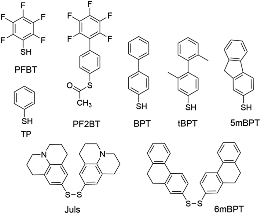 | ||
| Fig. 5 Molecular structures of sulfur compounds that are used to form SAMs for the modification of metal electrodes. | ||
Modification of metal electrodes with SAMs can also modulate nucleation and molecular orientation of semiconductor films deposited on the electrodes. As demonstrated by Gundlach et al. in 2008, the treatment of bottom-contact gold electrodes with PFBT was able to induce the growth of fluorinated 5,11-bis(triethylsilylethynyl)anthradithiophene (diF-TESADT in Fig. 4) on and from the SAM-treated contacts during the spin-coating process and their crystallites extended into the channel region leading to high-performance p-channel OTFTs and circuits.80 More recently, Amassian et al. modified bottom-contact gold electrodes with PFBT as well as other fluorinated phenylthiols, and investigated the interactions between the SAM-modified bottom contacts and the nucleation and growth of diF-TESADT and TIPS-PEN films as prepared by spin-coating and blade-coating processes.81 It is found that blade coating achieves texture purity in the films of diF-TESADT, irrespective of whether the contact is chemically treated with the SAM or not, in contrast to spin coating which requires the SAM to achieve favourable crystallization of organic semiconductors. These results suggest that previous design rules drawn from spin coating of organic semiconductors and contact-induced nucleation may have to be revisited in the context of blade coating. Briseno et al. modified the bottom-contact gold electrodes with PFBT in the vacuum-deposited OTFTs of rubicene.82 The SAM of PFBT not only significantly reduced the hole injection barrier from Au to rubicene from 1.15 to 0.48 eV due to the formation of a large interface dipole on Au, but also induced an “edge-on” configuration of rubicene favourable for charge transport.
Conclusions and perspectives
As discussed above, SAMs offer versatile ways to modulate the interfaces in OTFTs by chemically modifying the anchor group, the terminal group and the linker or by varying the conditions for adsorption and reaction of the SAM-forming molecules on the surface. Recent years have witnessed remarkable progress in SAMs as a very powerful platform for interface engineering of OTFTs. New SAMs with unprecedented terminal groups and frameworks have been designed and applied to manipulate the interface structures and properties in OTFTs leading to high-performance devices. On the basis of previous research on interface engineering for vacuum-deposited OTFTs on rigid substrates, more efforts have been devoted to solution-processed OTFTs and even devices on flexible substrates. A series of studies on structurally-related molecules have shed light on the relationship between SAM structures and OTFT performance. Nevertheless, the conclusions on the structure–property relationship as made on the basis of different molecular systems have shown controversies. A set of general guidelines for molecular design of SAMs is still a task to be completed for the interface engineering of OTFTs. The interfaces in the solution-processed OTFTs on flexible substrates have been less understood than those in the vacuum-deposited OTFTs on rigid substrates. The dielectric and electrode surfaces in solution-processed OTFTs and flexible devices should be a focus of the future research of interface engineering with SAMs. Moreover, through molecular design and organic synthesis, semiconductor backbones and a variety of functional groups can be grafted onto the SAMs leading to monolayer field effect transistors83,84 and allowing immobilization of binding sites85 for chemical and biological analytes. With such capability, SAMs may find more applications in OTFT-based chemical and biological sensing. We look forward to seeing new progress in the above directions in the near future.Conflicts of interest
There are no conflicts of interest to declare.Acknowledgements
The authors acknowledge financial support the Research Grants Council of Hong Kong (project number: GRF14303614), the National Natural Science Foundation of China (Grant No. 51603124), and the Science Foundation of Shenzhen University (No. 201502 and 827-000148).References
- T. Someya, A. Dodabalapur, J. Huang, K. C. See and H. E. Katz, Adv. Mater., 2010, 22, 3799 CrossRef CAS PubMed.
- G. Gelinck, P. Heremans, K. Nomoto and T. Anthopoulos, Adv. Mater., 2010, 22, 3778 CrossRef CAS PubMed.
- H. Dong, L. Jiang and W. Hu, Phys. Chem. Chem. Phys., 2012, 14, 14165 RSC.
- C. Di, Y. Liu, G. Yu and D. Zhu, Acc. Chem. Res., 2009, 42, 1573 CrossRef CAS PubMed.
- L. L. Chua, J. Zaumseil, J.-F. Chang, E. C.-W. Ou, P. K. H. Ho, H. Sirringhaus and R. Friend, Nature, 2005, 434, 194 CrossRef CAS PubMed.
- L. Li, K. Meise-Gresch, L. Jiang, C. Du, W. Wang, H. Fuchs and L. Chi, Adv. Mater., 2012, 24, 2053 CrossRef.
- C. Di, G. Yu, Y. Liu, X. Xu, D. Wei, Y. Song, Y. Sun, Y. Wang, D. Zhu, J. Liu, X. Liu and D. Wu, J. Am. Chem. Soc., 2006, 128, 16418 CrossRef CAS PubMed.
- Z. Li, J. Du, Q. Tang, F. Wang, J. Xu, J. C. Yu and Q. Miao, Adv. Mater., 2010, 22, 3242 CrossRef CAS PubMed.
- W. Wang, J. Han, J. Ying and W. Xie, IEEE Trans. Electron Devices, 2014, 61, 3507 CrossRef CAS.
- X. Chen, S. Zhang, K. Wu, Z. Xu, H. Li, Y. Meng, X. Ma, L. Liu and L. Li, Adv. Electron. Mater., 2016, 2, 1500409 CrossRef.
- J. C. Love, L. A. Estroff, J. K. Kriebel, R. G. Nuzzo and G. M. Whitesides, Chem. Rev., 2005, 105, 1103 CrossRef CAS PubMed.
- Y. D. Park, J. A. Lim, H. S. Lee and K. Cho, Mater. Today, 2007, 10, 46 CrossRef CAS.
- H. Ma, H. Yip, F. Huang and A. K.-Y. Jen, Adv. Funct. Mater., 2010, 20, 1371 CrossRef CAS.
- H. Ma, O. Acton, D. O. Hutchins, N. Cernetic and A. K.-Y. Jen, Phys. Chem. Chem. Phys., 2012, 14, 14110 RSC.
- S. Casalini, C. A. Bortolotti, F. Leonardi and F. Biscarini, Chem. Soc. Rev., 2017, 46, 40 RSC.
- F. Dinelli, M. Murgia, P. Levy, M. Cavallini and F. Biscarini, Phys. Rev. Lett., 2004, 92, 116802 CrossRef PubMed.
- M. Mas-Torrent and C. Rovira, Chem. Rev., 2011, 111, 4833 CrossRef CAS PubMed.
- X. Sun, C. Di and Y. Liu, J. Mater. Chem., 2010, 20, 2599 RSC.
- H. Ishii, K. Sugiyama, E. Ito and K. Seki, Adv. Mater., 1999, 11, 605 CrossRef CAS.
- J. Youn, G. R. Dholakia, H. Huang, J. W. Hennek, A. Facchetti and T. J. Marks, Adv. Funct. Mater., 2012, 22, 1856 CrossRef CAS.
- A. Ulman, Chem. Rev., 1996, 96, 1533 CrossRef CAS PubMed.
- D. K. Aswal, S. Lenfanta, D. Guerina, J. V. Yakhmib and D. Vuillaume, Anal. Chim. Acta, 2006, 568, 84 CrossRef CAS PubMed.
- S. P. Pujari, L. Scheres, A. T. M. Marcelis and H. Zuilhof, Angew. Chem., Int. Ed., 2014, 53, 6322 CrossRef CAS PubMed.
- M. D. Losego, J. T. Guske, A. Efremenko, J.-P. Maria and S. Franzen, Langmuir, 2011, 27, 11883 CrossRef CAS PubMed.
- M. D. Porter, T. B. Bright, D. L. Allara and C. E. D. Chidsey, J. Am. Chem. Soc., 1987, 109, 3559 CrossRef CAS.
- R. M. A. Azzam and N. M. Bashara, Ellipsometry and Polarized Light, North Holland, Amsterdam, 1977 Search PubMed.
- O. Acton, M. Dubey, T. Weidner, K. M. O'Malley, T.-W. Kim, G. G. Ting, D. Hutchins, J. E. Baio, T. C. Lovejoy, A. H. Gage, D. G. Castner, H. Ma and A. K.-Y. Jen, Adv. Funct. Mater., 2011, 21, 1476 CrossRef CAS.
- G. Nesher, A. Vilan, H. Cohen, D. Cahen, F. Amy, C. Chan, J. H. Hwang and A. Kahn, J. Phys. Chem. B, 2006, 110, 14363 CrossRef CAS PubMed.
- K. Fukuda, T. Hamamoto, T. Yokota, T. Sekitani and U. Zschieschang, Appl. Phys. Lett., 2009, 95, 203301 CrossRef.
- H. S. Lee, D. H. Kim, J. H. Cho, M. Hwang, Y. Jang and K. Cho, J. Am. Chem. Soc., 2008, 130, 10556 CrossRef CAS PubMed.
- Y. Chung, E. Verploegen, A. Vailionis, Y. Sun, Y. Nishi, B. Murmann and Z. Bao, Nano Lett., 2011, 11, 1161 CrossRef CAS PubMed.
- H. Chen, S. Dong, M. Bai, N. Cheng, H. Wang, M. Li, H. Du, S. Hu, Y. Yang, T. Yang, F. Zhang, L. Gu, S. Meng, S. Hou and X. Guo, Adv. Mater., 2015, 27, 2113 CrossRef CAS PubMed.
- D. O. Hutchins, T. Weidner, J. Baio, B. Polishak, O. Acton, N. Cernetic, H. Ma and A. K.-Y. Jen, J. Mater. Chem. C, 2013, 4, 101 RSC.
- J. Stöhr, NEXAFS Spectroscopy, Springer-Verlag, Berlin, 1992 Search PubMed.
- D. A. Outka, J. Stohr, J. P. Rabe and J. D. J. Swalen, Chem. Phys., 1988, 88, 4076 CAS.
- J. Stohr and D. A. Outka, Phys. Rev. B: Condens. Matter Mater. Phys., 1987, 36, 7891 CrossRef CAS.
- Y. Ito, A. A. Virkar, S. Mannsfeld, J. H. Oh, M. Toney, J. Locklin and Z. Bao, J. Am. Chem. Soc., 2009, 131, 9396 CrossRef CAS PubMed.
- D. Y. Kwok and A. W. Neumann, Adv. Colloid Interface Sci., 1999, 81, 167 CrossRef CAS.
- M. E. Schrader and G. I. Loeb, Modern Approaches to Wettability: Theory and Applications, Plenum Press, New York, 1992 Search PubMed.
- P. G. de Gennes, Rev. Mod. Phys., 1985, 57, 827 CrossRef CAS.
- K.-J. Chang, F. Y. Yang, C. C. Liu, M. Y. Hsu, T. C. Liao and H. C. Cheng, Org. Electron., 2009, 10, 815 CrossRef CAS.
- A. Vilan, D. Aswal and D. Cahen, Chem. Rev., 2017, 117, 4248 CrossRef CAS PubMed.
- W. Shao, H. Dong, L. Jiang and W. Hu, Chem. Sci., 2011, 2, 590 RSC.
- A. C. Mayer, J. M. Blakely and G. G. Malliaras, in Organic field-effect transistors, ed. Z. Bao and J. Locklin, Taylor & Francis Group, LLC, Boca Raton, 2007, ch. 5 Search PubMed.
- S. H. Kim, J. Lee, N. Park, H. Min, H. W. Park, D. H. Kim and H. S. Lee, J. Phys. Chem. C, 2015, 119, 28819 CAS.
- P. Maheshwari, S. Mukherjee, D. Bhattacharya, S. Sen, R. B. Tokas, Y. Honda, S. Basu, N. Padma and P. K. Pujari, ACS Appl. Mater. Interfaces, 2015, 7, 10169 CAS.
- J. Tsurumi, A. Yousefi Amin, T. Okamoto, C. Mitsui, K. Takimiya, H. Matsui, M. Halik and J. Takeya, Org. Electron., 2014, 15, 1184 CrossRef CAS.
- D. Liu, X. Xu, Y. Su, Z. He, J. Xu and Q. Miao, Angew. Chem., Int. Ed., 2013, 52, 6222 CrossRef CAS PubMed.
- D. Liu, Z. He, Y. Su, Y. Diao, S. C. B. Mannsfeld, Z. Bao, J. Xu and Q. Miao, Adv. Mater., 2014, 26, 7190 CrossRef CAS PubMed.
- X. Xu, Y. Yao, B. Shan, X. Gu, D. Liu, J. Liu, J. Xu, N. Zhao, W. Hu and Q. Miao, Adv. Mater., 2016, 28, 5276 CrossRef CAS PubMed.
- T. Minari, C. Liu, M. Kano and K. Tsukagoshi, Adv. Mater., 2012, 24, 299 CrossRef CAS PubMed.
- S. K. Park, D. A. Mourey, S. Subramanian, J. E. Anthony and T. N. Jackson, Adv. Mater., 2008, 20, 4145 CAS.
- T. Minari, M. Kano, T. Miyadera, S.-D. Wang, Y. Aoyagi, M. Seto, T. Nemoto, S. Isoda and K. Tsukagoshi, Appl. Phys. Lett., 2008, 92, 173301 CrossRef.
- K. P. Pernstich, S. Haas, D. Oberhoff, C. Goldmann, D. J. Gundlach, B. Batlogg, A. N. Rashid and G. J. Schitter, Appl. Phys., 2004, 96, 6431 CAS.
- C. Huang, H. E. Katz and J. E. West, Langmuir, 2007, 23, 13223 CrossRef CAS PubMed.
- F. D. Fleischli, S. Suárez, M. Schaer and L. Zuppiroli, Langmuir, 2010, 26, 15044 CrossRef CAS PubMed.
- S. Kobayashi, T. Nishikawa, T. Takenobu, S. Mori, T. Shimoda, T. Mitani, H. Shimotani, N. Yoshimoto, S. Ogawa and Y. Iwasa, Nat. Mater., 2004, 3, 317 CrossRef CAS PubMed.
- W. Yue, T. He, M. Stolte, M. Gsänger and F. Würthner, Chem. Commun., 2014, 50, 545 RSC.
- M. Nakano, I. Osaka and K. Takimiya, Adv. Mater., 2017, 29, 1602893 CrossRef PubMed.
- U. Kraft, U. Zschieschang, F. Ante, D. Kälblein, C. Kamella, K. Amsharov, M. Jansen, K. Kern, E. Weber and H. Klauk, J. Mater. Chem., 2010, 20, 6416 RSC.
- A. Y. Amin, K. Reuter, T. Meyer-Friedrichsen and M. Halik, Langmuir, 2011, 27, 15340 CrossRef CAS PubMed.
- C. Celle, C. Suspène, M. Ternisien, S. Lenfant, D. Guérin, K. Smaali, K. Lmimouni, J. P. Simonato and D. Vuillaume, Org. Electron., 2014, 15, 729 CrossRef CAS.
- D. H. Kim, Y. D. Park, Y. Jang, H. Yang, Y. H. Kim, J. I. Han, D. G. Moon, S. Park, T. Chang, C. Chang, M. Joo, C. Y. Ryu and K. Cho, Adv. Funct. Mater., 2005, 15, 77 CrossRef CAS.
- M. Novak, T. Schmaltz, H. Faber and M. Halik, Appl. Phys. Lett., 2011, 98, 093302 CrossRef.
- S. Hannah, J. Cardona, D. A. Lamprou, P. Šutta, P. Baran, A. A. Ruzaiqi, K. Johnston and H. Gleskova, ACS Appl. Mater. Interfaces, 2016, 8, 25405 CAS.
- O. Acton, G. G. Ting, P. J. Shamberger, F. S. Ohuchi, H. Ma and A. K.-Y. Jen, ACS Appl. Mater. Interfaces, 2010, 2, 511 CAS.
- M. Novak, C. M. Jäger, A. Rumpel, H. Kropp, W. Peukert, T. Clark and M. Halik, Org. Electron., 2010, 11, 1476 CrossRef CAS.
- Y. Lei, B. Wu, W.-K. E. Chan, F. Zhu and B. S. Ong, J. Mater. Chem. C, 2015, 3, 12267 RSC.
- B. Kang, N. Park, J. Lee, H. Min, H. H. Choi, H. S. Lee and K. Cho, Chem. Mater., 2015, 27, 4669 CrossRef CAS.
- P. Silberzan, L. Léger, D. Ausserré and J. J. Benattar, Langmuir, 1991, 7, 1647 CrossRef CAS.
- Z. Liang, Q. Tang, J. Xu and Q. Miao, Adv. Mater., 2011, 23, 1535 CrossRef CAS PubMed.
- X. Chen, Z. Xu, K. Wu, S. Zhang, H. Li, Y. Meng, Z. Wang, L. Li and X. Ma, Langmuir, 2016, 32, 9492 CrossRef CAS PubMed.
- D. Liu, Z. Li, Z. He, J. Xu and Q. Miao, J. Mater. Chem., 2012, 22, 4396 RSC.
- L. Miozzo, A. Yassar and G. Horowitz, J. Mater. Chem., 2010, 20, 2513 RSC.
- K. Asadi, F. Gholamrezaie, E. C. P. Smits, P. W. M. Blom and B. de Boer, J. Mater. Chem., 2007, 17, 1947 RSC.
- J. Roh, T. Lee, C. Kang, J. Kwak, P. Lang, G. Horowitz, H. Kim and C. Lee, Sci. Rep., 2017, 7, 46365 CrossRef CAS PubMed.
- O. Fenwick, C. V. Dyck, K. Murugavel, D. Cornil, F. Reinders, S. Haar, M. Mayor, J. Cornil and P. Samorì, J. Mater. Chem. C, 2015, 3, 3007 RSC.
- A. M. Masillamani, N. Crivillers, E. Orgiu, J. Rotzler, D. Bossert, R. Thippeswamy, M. Zharnikov, M. Mayor and P. Samorì, Chem. – Eur. J., 2012, 18, 10335 CrossRef CAS PubMed.
- M. Alt, M. Jesper, J. Schinke, S. Hillebrandt, P. Reiser, T. Rödlmeier, I. Angelova, K. Deing, T. Glaser, E. Mankel, W. Jaegermann, A. Pucci, U. Lemmer, U. H. F. Bunz, W. Kowalsky, G. Hernandez-Sosa, R. Lovrincic and M. Hamburger, Adv. Funct. Mater., 2016, 26, 3172 CrossRef CAS.
- D. J. Gundlach, J. E. Royer, S. K. Park, S. Subramanian, O. D. Jurchescu, B. H. Hamadani, A. J. Moad, R. J. Kline, L. C. Teague, O. Kirillov, C. A. Richter, J. G. Kushmerick, L. J. Richter, S. R. Parkin, T. N. Jackson and J. E. Anthony, Nat. Mater., 2008, 7, 216 CrossRef CAS PubMed.
- M. R. Niazi, R. Li, M. Abdelsamie, K. Zhao, D. H. Anjum, M. M. Payne, J. Anthony, D.-M. Smilgies and A. Amassian, Adv. Funct. Mater., 2016, 26, 2371 CrossRef CAS.
- H. Lee, Y. Zhang, L. Zhang, T. Mirabito, E. K. Burnett, S. Trahan, A. R. Mohebbi, S. C. B. Mannsfeld, F. Wudl and A. L. Briseno, J. Mater. Chem. C, 2014, 2, 3361 RSC.
- G. S. Tulevski, Q. Miao, M. Fukuto, R. Abram, B. Ocko, P. Pindak, C. Kagan and C. Nuckolls, J. Am. Chem. Soc., 2004, 126, 15048 CrossRef CAS PubMed.
- E. C. P. Smits, S. G. J. Mathijssen, P. A. van Hal, S. Setayesh, T. C. T. Geuns, K. A. H. A. Mutsaers, E. Cantatore, H. J. Wondergem, O. Werzer, R. Resel, M. Kemerink, S. Kirchmeyer, A. M. Muzafarov, S. A. Ponomarenko, B. deBoer, P. W. M. Blom and D. M. de Leeuw, Nature, 2008, 455, 956 CrossRef CAS.
- W. Huang, K. Besar, R. LeCover, P. Dulloor, J. Sinha, J. F. Martínez Hardigree, C. Pick, J. Swavola, A. D. Everett, J. Frechette, M. Bevand and H. E. Katz, Chem. Sci., 2014, 5, 416 RSC.
Footnote |
| † We dedicate this paper to Prof. Daoben Zhu on the occasion of his 75th birthday. |
| This journal is © the Partner Organisations 2018 |