
 Open Access Article
 This Open Access Article is licensed under a
 Creative Commons Attribution 3.0 Unported Licence
Lifetime and nonlinearity of modulated surface plasmon for black phosphorus sensing application
Renlong
Zhou
 *a,
Jing
Peng
a,
Sa
Yang
*a,
Dan
Liu
a,
Yingyi
Xiao
a and
Guangtao
Cao
*b
*a,
Jing
Peng
a,
Sa
Yang
*a,
Dan
Liu
a,
Yingyi
Xiao
a and
Guangtao
Cao
*b
aSchool of Physics and Information Engineering, Guangdong University of Education, Guangzhou 510303, China. E-mail: yangs7014@sina.com; rlzhoupc@sina.com
bCollege of Physics, Mechanical and Electrical Engineering, Jishou University, Jishou 416000, China. E-mail: caoguangtao456@126.com
First published on 2nd October 2018
Abstract
Black phosphorus surface plasmon (BPSP) is a new promising candidate material for electromagnetic field confinement at the subwavelength scale. Here, we theoretically investigated the light confinement, second-order nonlinearity and lifetimes of tunable surface plasmons in nanostructured black phosphorus nanoflakes with superstrates. The grating structure can enhance the local optical field of the fundamental wave (FW) and second harmonic wave (SHW) due to the surface plasmon resonance. Based on the coupled mode theory (CMT), a theoretical model for the nanostructured black phosphorus was established to study the spectrum features of FW. The lifetimes of the plasmonic resonant modes were investigated with the finite difference time domain (FDTD) simulations and CMT. Since the permittivity of black phosphorus depends on its Fermi energy and electron scattering rate, the lifetimes of plasmonic absorption modes are tunable with both the Fermi energy and scattering rate. The intensity, wavelengths and spectral width of BPSP resonance modes and their lifetimes can be precisely controlled with the Fermi energy, scattering rate, side length and refractive index of the superstrate. The sensitivity is described by varying the refractive index of the superstrate such as an aqueous solution. We have introduced a second-order nonlinear source to investigate the SHW of nanostructured black phosphorus. This paper presents the corner/edge energy distribution and the tunable lifetime of BPSP as well as their unprecedented capability of photon manipulation for second-order nonlinearity within the deep subwavelength scale. The configuration and method are useful for research of the absorption, lifetime of light and nonlinear optical processes in black phosphorus-based optoelectronic devices, especially the modulation and sensing applications.
1. Introduction
Black phosphorus (BP), a two-dimensional (2D) plasmonic material, has shown great promise in atomic scale light–matter interaction for applications such as photonics, imaging, sensing, optoelectronics and telecommunications.1–4 Due to the decent carrier mobility of ∼1000 cm2 V−1 s−1 and the finite bandgap of ∼0.3 eV, black phosphorus acts as a suitable candidate, attracting increasing attention in the design of absorbers.5–7 Black phosphorus-based saturable absorbers are used to achieve pulse emission of lasers, Q-switching, and mode locking.8 The 2D black phosphorus, with puckered hexagonal honeycomb structure having ridges of atoms, has strong in-plane anisotropic electrical and optical properties.9,10 Black phosphorus has a thickness-dependent direct bandgap ranging up to ∼2 eV, which could possess broadband photoresponse from the mid-IR to far-IR and even the visible band.11,12 The direct bandgap and plasmon of black phosphorus can be tuned with electric voltage bias, even for more than 20 layers. The black phosphorus plasmonic properties and unprecedented capability of wide-band photon manipulation have been presented within the deep subwavelength scale.13 Compared with traditional bulk plasmonic materials, it is possible to integrate devices on the atomic scale using few-layer black phosphorus due to highly localized electric fields.14 Highly confined and electrically tunable graphene plasmons, such as electromagnetically induced transparency, and Fano resonance, have been studied below the classical diffraction limit.15 The dipole-like interactions have been observed in 2D graphene materials due to the localized surface plasmon (LSP) resonance effect (the collective oscillations of charged carriers).16,17 Most of the studies on black phosphorus have concentrated on the electrical and linear optical properties, with only a few studies on the nonlinear optical properties that are mainly related to nonlinear saturable absorption and anisotropic third harmonic generation from exfoliated black phosphorus.18–23 The enhancement of the fundamental wave and second harmonic wave has been observed in metallic structures and nanostructured metal or graphene.24–34 Experiments and theories have shown that linear transmission through arrays is sensitive to many factors such as array periodicity, hole shape and size, incidence angle, and film thickness. For instance, the experimental observations of the SHG signal have also been reported.25 Methods of enhancing the SHG were widely studied by double plasmonic resonance, Fano resonance, and even nanocup structure.31 They measured the SHG from a periodic array using femtosecond laser pulses and observed the SHG signal intensity. Particularly they measured the propagation time duration of the pulses through the array to clarify the slow light effect. Modulated black phosphorus surface plasmon offers a promising way to realize chip-scale integrated photonic circuits because of their ability to confine and control electromagnetic waves at the subwavelength scale with strong confinement of surface plasmon. It was found that some challenges such as serious scattering loss, which is caused by the substrate, boundary and absorbents, limit the mode lifetime, plasmon propagation length and spectral range. For the black phosphorus, it is imperative to investigate the localized surface plasma properties and their lifetime. The findings provide a possibility to realize black phosphorus-based optoelectronic devices that are highly photoresponsive, wavelength selectable and lifetime tunable. The fabrication of layered BP, especially phosphorene, may pave the way towards the realization of high-performance nano-devices, photodetectors and other photothermal properties.35 The peak position and bandwidth of the phosphorene absorption spectra are tunable via the surrounding dielectric environment of the periodic nanoribbons.36In this paper, we numerically analyze the confined surface plasmon of the fundamental wave and the second harmonic wave in the nanostructured black phosphorus nanoflake, which forms a grating to enhance the light–matter interaction. Coupling of light from the normal direction with nanostructured black phosphorus requires an arbitrary grating coupler providing lateral photon momentum. We present a CMT analysis based on the cavity theory that describes the linear resonant modes of the cavity systems.37,47 The linear absorption spectra for various Fermi energies, the electron scattering rate, side length of black phosphorus and the refractive indexes of superstrates with the FDTD method agree well with the theoretical description. Lifetime is important for the research of intrinsic loss for the mth mode and interaction between each mode and light field. The lifetimes of plasmonic absorption modes are tunable with the Fermi energy, the scattering rate, side length of black phosphorus and refractive index of the superstrate. The intensity, wavelengths and spectral width of BPSP resonance modes can be precisely controlled. Moreover, the sensitivity is demonstrated by varying the refractive index n1 of the superstrate such as an aqueous solution. The second-order nonlinearity in nanostructured black phosphorus is achieved due to the symmetry breaking. With the introduction of the second-order nonlinear source, we investigate the second-order nonlinearity such as second harmonic generation (SHG), sum frequency generation (SFG) and difference frequency generation (DFG). The methods are useful for investigating the lifetime of light and nonlinear optical processes in black phosphorus-based optoelectronic devices, especially the black phosphorus modulation and sensing applications.38–42
2. The coupled BPSP system and theoretical analysis
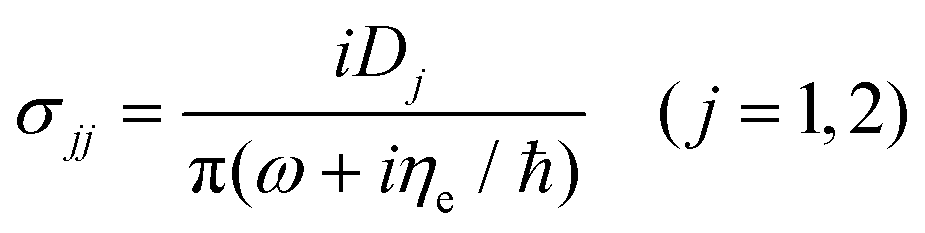
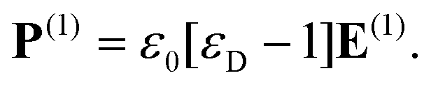
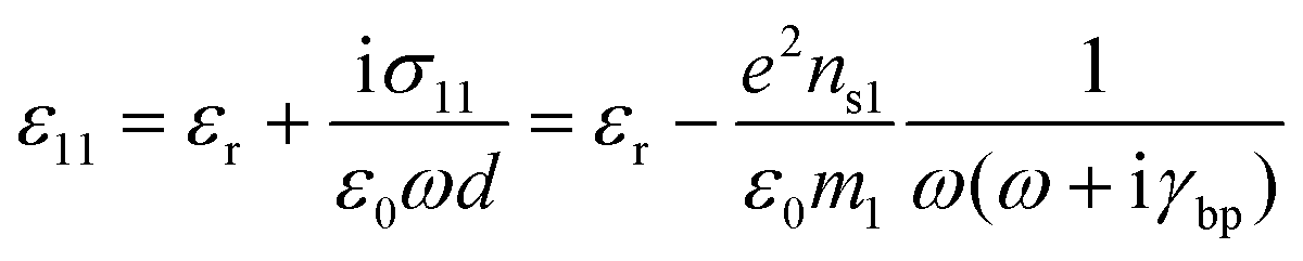
We consider a nanostructured black phosphorus nanoflake, formed by the black phosphorus square array, which is composed of the elementary cell with period P = 200 nm in the xy-plane. The black phosphorus square array is placed on the SiO2 substrate and covered with a superstrate such as an aqueous solution in Fig. 1(a). The black phosphorus nanoflake has the cuboid shape (length × width × thickness) with L × L × d. The parameters of the black phosphorus flake are set as follows: side length L = 150 nm and thickness d = 2 nm. The refractive index of the superstrate is n1 in the model. The permittivity of a 2D black phosphorus layer can be characterized as a diagonal tensor.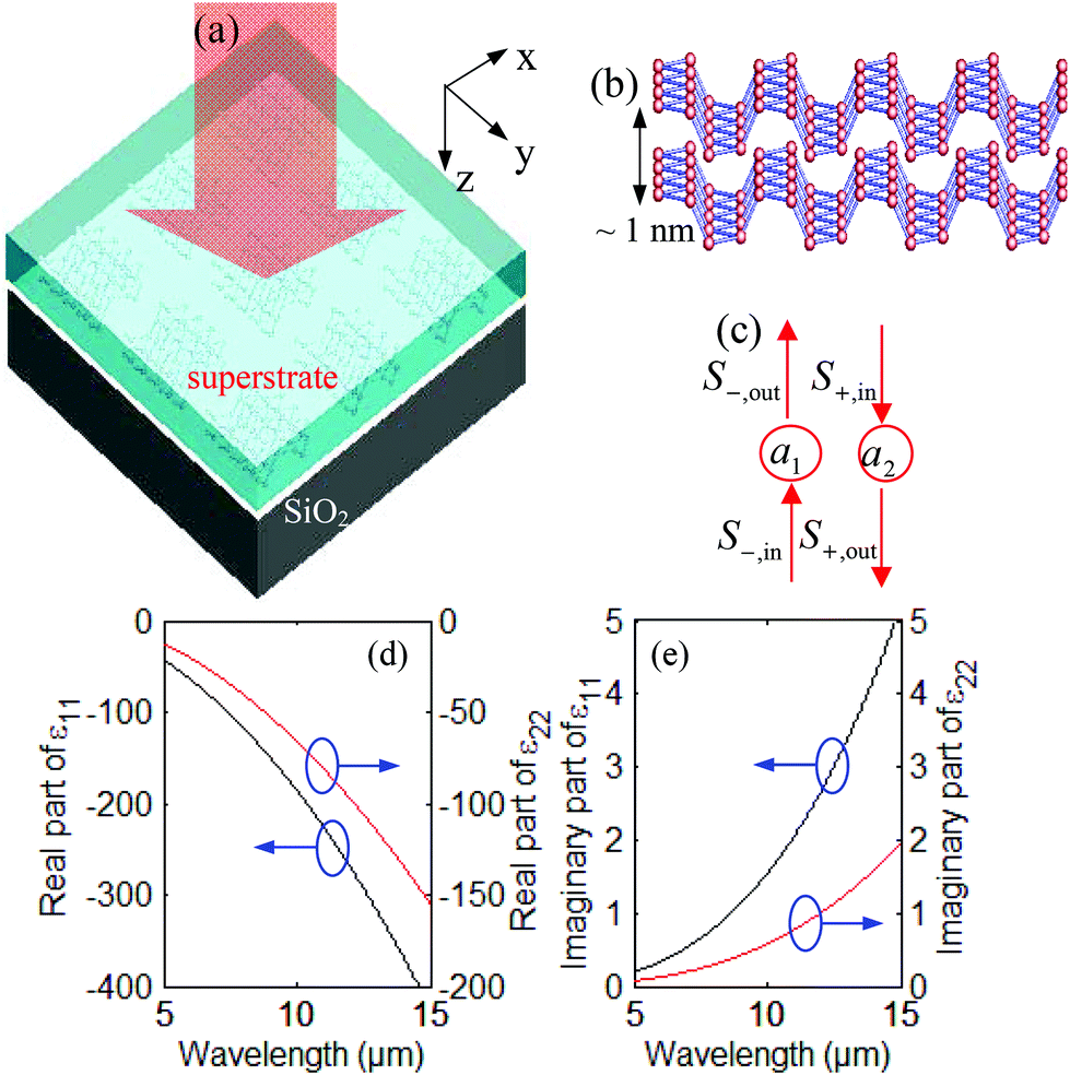 | ||
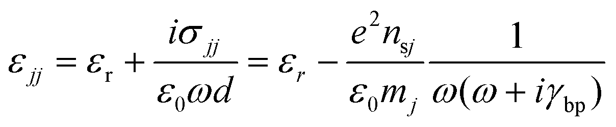
| Fig. 1 (a) The nanostructured black phosphorus nanoflake on SiO2 substrate. The input light wave is polarized along the x-direction and propagates along the z-direction. (b) Side view of the black phosphorus flake. (c) The CMT model with two resonant modes of the nanostructured black phosphorus system. (d) The real part and (e) imaginary part of the relative permittivity tensor component ε11 and ε22, respectively. | ||
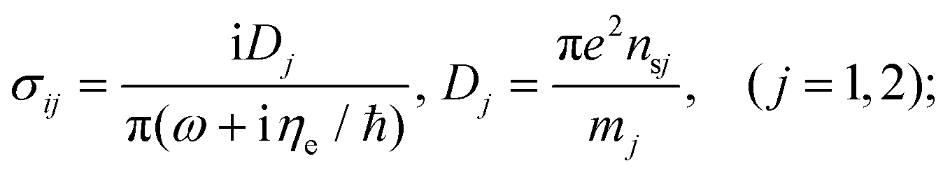
All simulations are carried out for photon energies of up to 0.7 eV,12,17,18,36 the bandgap of BP. Within this energy window, the Drude model is sufficient to model the conductivity of the multilayer BP system. The conductivity of few-layer black phosphorus is given as7,12–15,36
 | (1) |
We can introduce a phosphorene layer with volumetric anisotropic permittivity converting the 2D surface conductivity into a 3D conductivity using the relation σ2D = d σ3D.36 The equivalent relative permittivity diagonal tensor εD(ε11, ε22, ε33) is defined to describe the black phosphorus with thickness d. The equivalent relative permittivity tensor for the in-plane component of black phosphorus is given by the following:
 | (2) |
For nanostructured black phosphorus, the parameters of the conduction band can be set as follows: the thickness-dependent direct band gap Δ is about 0.7 eV for thickness d = 2 nm, γ = 4a/π eV m (a = 0.223 nm is the scale length), ηc = ħ2/(0.4m0), vc = ħ2/(0.7m0), ηe = 10−3 eV, and Ef − Ec = 0.6 eV; electron mass m0 = 9.10938 × 10⁻³¹ kg.
The real part and imaginary part of the relative permittivity component ε11 and ε22 are shown in Fig. 1(d) and (e), respectively. The corresponding data for conductivity and relative permittivity tensor components have been reported in the literature.7,13–15,36
The characteristics of the BPSP in nanostructured black phosphorus can be analyzed with the CMT method as shown in Fig. 1(c). When the light wave S+,in passes through the black phosphorus grating, the energy can be coupled into the black phosphorus grating due to the SPR effect. The resonance modes of BPSP can be inspired by the energy amplitude am (m = 1,2) in the whole region of the black phosphorus grating, where dam/dt = −iωam. am is the mth mode of resonant modes with resonance frequency ωm. km stands for the coupling between cavity modes. The incoming and outgoing waves are depicted by S±,in(out). The energy amplitude a1 and a2 of the BPSP resonators can be expressed as follows:37,47
 | (3) |
| S+out = −S−in + 〈K|a〉, | (4) |
| S−out = −S+in + 〈K|a〉. | (5) |
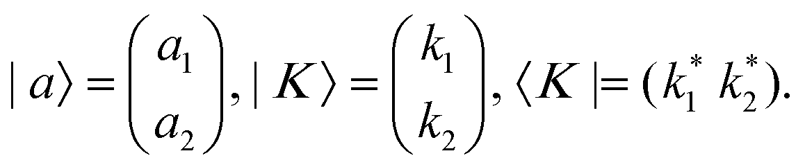
|a〉 and |K〉 represent the field amplitude of the resonant mode and the coupling coefficient between resonators, respectively. 〈K| is dependent on |K〉. They can be written as
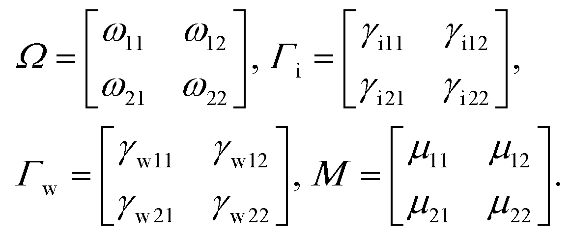
In eqn (3), Ω, Γi, Γe, and M matrixes are given as
 | (6) |
 | (7) |
| A(ω) = 1 − |t|2 − |r|2. | (8) |
The derived expression A(ω) in eqn (8) with CMT includes the parameters ωm, τim, τwm, μ12, and μ21, which are used to describe the absorbance of black phosphorus. The resonant wavelength λm (m = 1,2) can be obtained from the FDTD simulation. The parameter ωm (m = 1,2) in eqn (8) can be obtained using ωm = 2πc/λm. After choosing the appropriate parameters of 1/τim, 1/τwm, μ12 and μ21, we can precisely compare the intensity, resonant wavelength and spectral width of the resonance absorption peaks A(ω) obtained by CMT with that of the absorption spectrum simulated by the FDTD method; we can then derive the value of these parameters such as ωm, 1/τim and 1/τwm.
The second-order nonlinearity in nanostructured black phosphorus is described by the nonlinear Lorentz force acting on the black phosphorus electrons. The nonlinear theory has been formulated based on the Vlasov–Maxwell equations. The first thing is the source of SHW. SHW comes from a second-order nonlinear process originating from the surface atoms of the black phosphorus grating, where the broken spatial inversion symmetry will lead to non-zero second-order nonlinear susceptibility. The illumination of the high peak power femtosecond pulse laser upon the black phosphorus will induce second-order nonlinear polarization, which will radiate SHW.31
The second-order nonlinearity in nanostructured black phosphorus is described by the nonlinear Lorentz force acting on the black phosphorus electrons. The nonlinear theory has been formulated based on the Vlasov–Maxwell equations. The equation of the second-order nonlinear source in the black phosphorus grating can be described as follows:24
 | (9) |
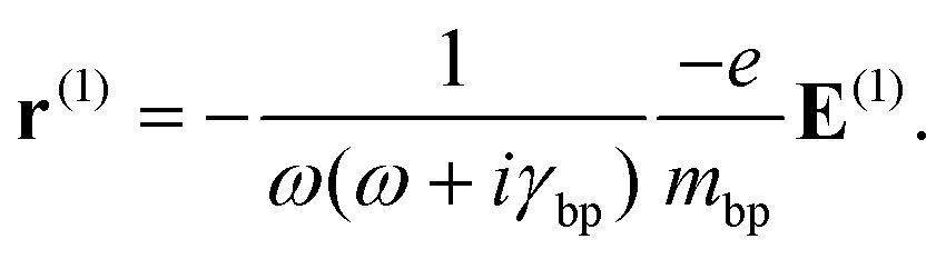
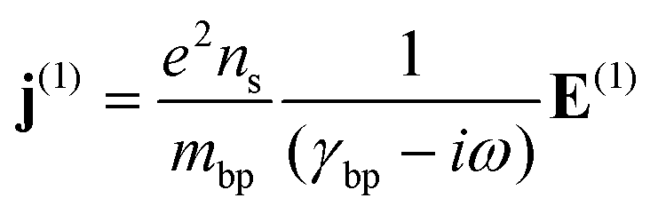
Here, j(2)z = 0, k represents the x, y, and z coordinates; n0 and me stand for the black phosphorus-ion density and effective electron mass in the black phosphorus grating, respectively. The S(2) is the second-order nonlinear source. There are two second-order contributions to nonlinear optics, one is the electric part of the Lorentz force ρ(1)E(1). The surface charge density ρ(1) appears, which diminishes the normal component of the electric field E(1) inside the black phosphorus. Another contribution is the magnetic part of the Lorentz force j(1) × B(1). The moving electrons are mainly located inside the skin depth of the black phosphorus. Due to the penetrating magnetic field B(1), the moving electrons feel the magnetic part of the Lorentz force.
3. Fundamental wave and second harmonic wave
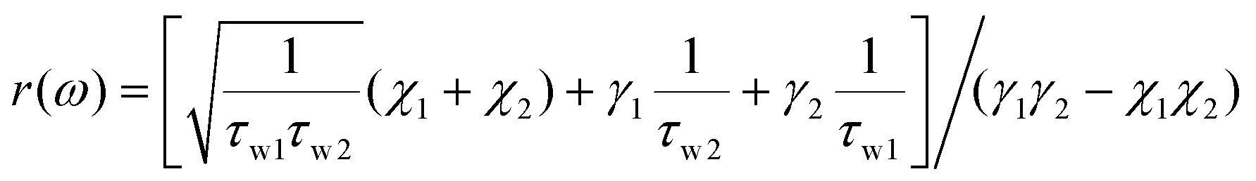
Light can be coupled into the nanostructured black phosphorus flake from the normal direction. There is a propagating wave inside the black phosphorus flake with an effective wavelength matching the grating period. The electric field of the incident light is oriented across the black phosphorus flake. The surface plasmon resonance can be excited if the frequency of the incident light matches the grating period. To study the optical properties in the square array of the black phosphorus flake in Fig. 1(a), the normalized linear-optical absorption (black circles) of FW through the nanostructured black phosphorus flake is investigated with FDTD simulation as shown in Fig. 2(a). Here, the parameters are set as P = 200 nm, L = 150 nm, and d = 2 nm, ηe = 10−3 eV, and Ef − Ec = 0.6 eV. The red line represents the theoretical CMT result in Fig. 2(a). There are two BPSP resonance modes with the first resonant mode at wavelength λ1 = 7.7 μm and the second resonant mode at wavelength λ2 = 9.7 μm. The two BPSP resonance modes originate from the dipole resonance, which exists due to the collective oscillations of charged carriers. The parameter ωm (m = 1,2) in eqn (8) can be obtained with ωm = 2πc/λm. The absorption spectra A(ω) in eqn (8) can be obtained with appropriate parameters 1/τw1, 1/τw2, 1/τi1, 1/τi2, μ12 and μ21. We can precisely compare the intensity, resonant wavelength and spectral width of the resonance absorption peaks A(ω) obtained by CMT with that of the absorption spectrum simulated by the FDTD method in Fig. 2(a). Then, we can obtain the parameters in eqn (8) with 1/τw1 = 8.6 × 10¹⁰ rad s−1, 1/τw2 = 7.3 × 10¹⁰ rad s−1, 1/τi1 = 1.41 × 10¹² rad s−1, 1/τi2 = 5.3 × 10¹² rad s−1, μ12 = μ21 = 1011 rad s−1. We suppose that the coupling coefficients μ12 and μ12 are unchanged in the model. The theoretical CMT results (red line) are in good agreement with the results using FDTD simulation (black circles), which can ensure the precise adjustment of the BPSP. The larger spectral width is directly related to the shorter pulse length. The electric field distribution of the individual resonances overlaps spatially, which leads to a coupling of the two resonances. The key feature of the black phosphorus grating is the coupling of a photonic resonance with an electric resonance. | ||
| Fig. 2 (a) The linear-optical absorption with FDTD simulation (black circles) and the theoretical CMT (red line). The distribution of (b) charge density σ(1), (c) corresponding electric field E(1)x and (d) corresponding total electric field intensity |E(1)|2 for the FW at resonant wavelength λ1 = 7.7 μm; (e) charge density σ(1), (f) corresponding electric field E(1)x and (g) corresponding total electric field intensity |E(1)|2 at wavelength λ2 = 9.7 μm. | ||
An important aspect of a black phosphorus plasmon is that it generally comprises an electric dipole moment. An incident electromagnetic wave can couple to the dipole and excite the corresponding plasmon oscillation. The oscillating dipole radiates and the associated energy loss significantly broadens the linewidth of the emission spectrum. The electric field inside the black phosphorus is a superposition of a wave decaying on the order of the skin depth and depolarization field. In the case of black phosphorus plasmons, which also comprise a magnetic dipole moment, the linear-optical coupling strength of the electric field to the plasmon is usually stronger than that of the magnetic field.
For varying ε(r) (i.e., ∇ε ≠ 0) in the nanostructured black phosphorus, there is ρ(1,2) = ∇·D(1,2) ≠ 0 in the region of black phosphorus, and ρ(1,2) is the bulk charge density for FW and SHW. The spectra stem from the fact that waves satisfy ∇·D(1,2) ≠ 0 and may induce electric charge oscillation ρ(1)(r)eiωt or ρ(2)(r)ei2ωt. On the surface of black phosphorus, D(1,2)z has abrupt discontinuity across the boundary. The boundary condition is n·D(1,2)zz = σ(1,2) where z is the unit vector along the z-direction and n = nz. σ(1,2) is the surface charge density for FW and SHW, respectively. The dipole-like interactions have been observed in nanostructured black phosphorus nanoflake due to the LSP resonance effect.
The distributions of charge density σ(1) and corresponding electric field E(1)x for the FW at the resonant wavelength λ1 = 7.7 μm are shown in Fig. 2(b) and (c), respectively. Inside the black phosphorus, one dipole is arranged at the left and right edges corresponding to the polarization of the incident light in Fig. 2(b). The patterns of charge density σ(1) at the left and right edges of black phosphorus are nearly the same, but they have opposite signs that are labeled as ±. The distribution of surface charge density σ(1) in black phosphorus grating is consistent with the local charge dipole oscillations. The electric field E(1)x at wavelength 7.7 μm is seen to be entirely localized inside the black phosphorus region and the edge along the x-direction as shown in Fig. 2(c). Seemingly, the dipole in Fig. 2(b) is flanged by the opposite surface charge and the charges establish a standing BPSP resonance inside the black phosphorus region and edge along the x-direction in Fig. 2(c). Strong localization in the C1 region indicates that the C1 region is the principal channel of the energy transportation. After the absorption of the incident wave, a local field locates at the surface of the black phosphorus. This field component is associated with a non-zero charge density near the interface, and its magnitude decays very fast outside the black phosphorus, approximately on the scale of a Thomas–Fermi screening length, which is about 6 nm for black phosphorus.36
The charge density σ(1) and corresponding electric field E(1)x for the FW at resonant wavelength λ2 = 9.7 μm are seen to be strongly located at the four corners of the black phosphorus as shown in Fig. 2(e) and (f), which is a typical corner effect. Inside one black phosphorus, two dipoles are arranged at the corners due to the corner effect. Seemingly, the two dipoles are flanged by opposite surface charges that are labeled as ± in Fig. 2(e). These charges establish a standing wave resonance along the edge region of the black phosphorus in Fig. 2(f). Strong localization in the C2 region indicates that the C2 region is the principal channel of the energy transportation. The electric field E(1)x has the exponential decay out of the black phosphorus flake.
The black phosphorus flake has mirror symmetry with respect to the x-axis for the fundamental wave. After the consideration with the polarization along the x-axis, we have the following two relations: anti-symmetrical charge density σ(1)(−x,y,z) = −σ(1)(x,y,z) and the corresponding symmetrical electric field E(1)x(−x,y,z) = E(1)x(x,y,z).
Total electric field intensity (|E(1)|2) profile shown in Fig. 2(d) implies that the total electric field intensity (|E(1)|2) is mostly localized at the left and right edges corresponding to the polarization of the light and four corners for resonant wavelengths λ1 = 7.7 μm.14 The electric field intensity for resonant wavelengths λ2 = 9.7 μm is mostly localized around the four corners of the square due to the sharpness in shape in Fig. 2(g).
Beyond these fascinating linear-optical effects, the black phosphorus grating promises unprecedented phenomena in nonlinear optics. The excitation of BPSP produces a strong enhancement of the electric field in the surface. The generation of second harmonics in these enhanced fields is also expected. If the square array of black phosphorus flakes is irradiated with monochromatic light, the SHW can be excited in resonance.
In black phosphorus, the linear polarization P(1) = (−e)nsr(1) can be related to electrons with charge (−e) and density (ns) being displaced by r(1) from their equilibrium position. Illumination with an electromagnetic plane wave oscillating with a single frequency ω0 thus results in an electron velocity v(1) = ∂r(1)/∂t. In the simplest case, the velocity v(1), the polarization P(1) and the incident local electric field E(1) have the same direction, which in turn is perpendicular to the Bloch wave vector k. Furthermore, if the electrons can be viewed individually, the local magnetic field B(1) at the position of an electron corresponds to the value and orientation of the local electric field, hence B(1) ∝ k × E(1).
It is obvious that such an electron feels the magnetic part of the Lorentz force FL,m = (−e) v(1) × B(1), which is of second order in perturbation. The second-order oscillation r(2) at frequency 2ω0 resulting from this force can lead to SHW radiation. With the electric dipole approximation, the electric field of SHW can be related to the electric field of the FW such that24
| E(2)(2ω1, 2ω2,ω2 − ω1, ω2 + ω1) ∝ χ(2)·E(1)(ω1)E(1)(ω2) | (10) |
For the incident continuous wave with two frequencies ω1 and ω2, the linear electromagnetic field can be given by E(1)(r,t) = E(1)0(r) (e−iω1t + e−iω2t). Thus, the second order source S(2) in eqn (9) can be described as S(2) ∝ S(2)1e−i2ω1t + S(2)2e−i2ω2t + S(2)3e−i(ω1+ω1)t − S(2)4cos(ω2 − ω1)t + S(2)5sin(ω2 − ω1)t, where S(2)1,2,3,4,5 are the amplitudes. There are frequency components 2ω1, 2ω2, ω2 + ω1 and ω2 − ω1 in the expressions of the second order source; that is to say, it has second-order nonlinearity such as SHG, SFG and DFG.
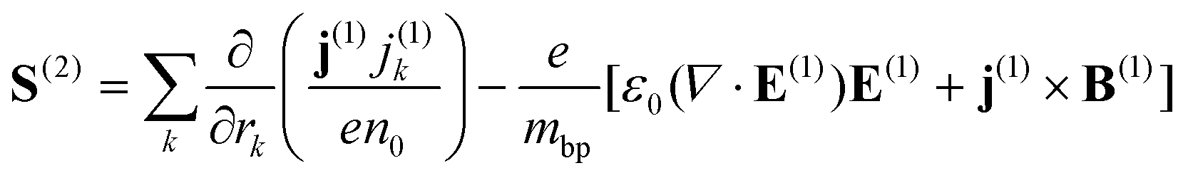
In the case of the incident wavelengths, λ1 = 7.7 μm and λ2 = 9.7 μm in Fig. 3(a), we can obtain the second-order nonlinearity including SHG as well as the SFG and DFG in Fig. 3(b). For the FW wave propagating away from the substrate, the amplitude of the Fourier spectrum for E(1)x with two different wavelengths, λ1 = 7.7 μm and λ2 = 9.7 μm, is shown in Fig. 3(a). For the SHW wave propagating away from the substrate, the amplitude of the Fourier spectrum for E(2)x is shown in Fig. 3(b). It is noted that there are four peaks for the second-order nonlinear spectrum with the four resonant wavelengths λ3 = 3.85 μm, λ4 = 4.85 μm, λ5 = 4.3 μm, and λ6 = 38.1 μm in Fig. 3(b), respectively. The larger spectral width for wavelength λ6 is directly related to the shorter pulse length of the nonlinear fields. The distributions of total electric field intensity (|E(2)|2) at four resonant wavelengths (c) λ3 = 3.85 μm, (d) λ4 = 4.85 μm, (e) λ5 = 4.3 μm, and (f) λ6 = 38.1 μm are shown in Fig. 3. The total electric field intensity (|E(2)|2) for resonant wavelength λ3 = 3.85 μm is mostly localized at the left and right edges corresponding to the polarization of the light. The total electric field intensity (|E(2)|2) for the resonant wavelength λ4 = 4.85 μm is mostly localized at the left and right edges and center surface region. The total electric field intensity (|E(2)|2) for resonant wavelength λ5 = 4.3 μm is mostly localized at the four edges. The total electric field intensity (|E(2)|2) for resonant wavelength λ6 = 38.1 μm is mostly localized at the four corners.
 | ||
| Fig. 3 (a) The amplitude of the Fourier spectrum for FW E(1)x with two wavelengths λ1 = 7.7 μm and λ2 = 9.7 μm, (b) the amplitude of the Fourier spectrum for SHW E(2)x with the four wavelengths λ3, λ4, λ5, and λ6. The distribution of total electric field intensity |E(2)|2 at resonant wavelength (c) λ3, (d) λ4, (e) λ5, and (f) λ6, respectively. The plots of charge density σ(2) and (e) corresponding electric field E(2)x at resonant wavelength λ3, λ4, λ5, and λ6 are shown in (g)–(n), respectively. | ||
We find that the second-order nonlinearity modes at wavelengths λ3 = 3.85 μm and λ4 = 4.85 μm are obtained from the incident monochromatic wave with wavelengths λ1 = 7.7 μm and λ2 = 9.7 μm due to the SHG effect, respectively. The second-order nonlinearity mode at wavelength λ5 = 4.3 μm is the sum-frequency field signal for the FW with wavelengths λ1 and λ2. The second-order nonlinearity mode at wavelength λ6 = 38.1 μm is the difference-frequency field for the FW with two resonant wavelengths λ1 and λ2. The SHW conversion efficiency η is defined in the nonlinear optical process as the expression η = |E(2)(2ω0)/E(1)(ω0)|. The second-order nonlinear conversion efficiency for the FW with two resonant wavelengths is about 10−11. The strongly localized field and non-centrosymmetry can induce an increase in second harmonic nonlinearity signals.
The distributions of charge density σ(2) and corresponding electric field E(2)x for the SHW at the resonant wavelength λ3 are shown in Fig. 3(g) and (h), respectively. Charge density σ(2) is mainly located at the left and right edges corresponding to the polarization of the light. The patterns of charge density σ(2) at the left and right edges of black phosphorus are nearly the same, and they have the same signs which are labeled as ±. The distribution of surface charge density σ(2) in the black phosphorus grating is consistent with the local charge dipole oscillations. The corresponding electric field E(2)x at wavelength λ3 is shown in Fig. 3(h). Seemingly, the charges density σ(2) in Fig. 3(g) is flanged by the opposite surface charge and the charges establish a standing BPSP resonance inside the black phosphorus region in Fig. 3(h). Moreover, the standing BPSP resonance has the exponential decay out of the edge along the x-direction in Fig. 3(h). The distributions of charge density σ(2) and corresponding electric field E(2)x at wavelength λ4 are shown in Fig. 3(i) and (j), respectively. The electric field E(2)x is seen to be entirely localized inside the black phosphorus region in Fig. 3(j). The distributions of charge density σ(2) and corresponding electric field E(2)x at the wavelength λ5 are depicted in Fig. 3(k) and (l), respectively. Charge density σ(2) is mainly located at the four edges. The electric field E(2)x is seen to be entirely localized inside the two edge regions along the y-direction, and the electric field E(2)x has the exponential decay out of the edge along the x-direction in Fig. 3(l). The distributions of charge density σ(2) and corresponding electric field E(2)x at the wavelength λ6 are shown in Fig. 3(m) and (n), respectively. Charge density σ(2) is mainly located at the four corners, four edges and the center region. The dipole-like interactions have been observed in Fig. 3(n) due to the LSP resonance effect.
The black phosphorus flake has mirror symmetry with respect to the x-axis for the second harmonic wave. After the consideration with the polarization along the x-axis, we have the following two relations: symmetrical charge density σ(2)(−x,y,z) = σ(2)(x,y,z) and the corresponding anti-symmetrical electric field E(2)x(−x,y,z) = −E(2)x(x,y,z). The symmetry of charge density σ(2) and corresponding electric field E(2)x is different from that of charge density σ(1) and corresponding electric field E(1)x. The second harmonic wave results from the dipole-like interactions due to the LSP resonance effect (the collective oscillations of anti-symmetrical charge density σ(1)).
4. Modulation and sensing application
The intensity, wavelengths and spectral width of resonance peaks can be precisely modulated with the Fermi energy, scattering rate ηe and side length L of BP. The black phosphorus square array is covered with the superstrate of an aqueous solution, and the sensitivity is demonstrated by varying the refractive index n1 of the superstrate. A significant enhancement of the chemical or gas sensing performance of noble metal incorporated BP systems has been reported.38,39 The BPSP resonance performance can also be enhanced in a black phosphorus nanoflake grating compared to that in a single black phosphorus nanoflake.48First, we investigate the change in BPSP in black phosphorus by varying the relative Fermi energy Ef − Ec, which can be adjusted with applied voltage bias or doping concentration.40,41 The parameter ηe is fixed with 0.001 eV for various relative Fermi levels Ef − Ec. The absorption spectra with different relative Fermi energies (a) Ef − Ec = 0.7 eV, (b) Ef − Ec = 0.5 eV, and (c) Ef − Ec = 0.3 eV are shown in Fig. 4 by the CMT theory (red line) and FDTD method (black circles), respectively. With the increment of relative Fermi energy Ef − Ec, the absorption of the first resonant wavelength will get higher while the absorption of the second resonant wavelength will become lower as seen in Fig. 4(a)–(c); the two resonance modes shift to shorter wavelength with increasing Fermi energy. The shift of resonance wavelength and the change in absorption amplitude can be elaborated by CMT theory. The intensity, wavelengths and spectral width of resonance peaks with the FDTD method are in good agreement with the theoretical CMT results. The evolution of simulated linear-optical absorption spectra for different relative Fermi energies Ef − Ec is presented in Fig. 4(d). With the relative Fermi energy of black phosphorus tuned in the range of 0.15–0.8 eV, the first resonance mode can be modulated in the range of 7.1–15 μm while the second resonance mode can be modulated in the range of 8.5–15 μm. This response characteristic in Fig. 4(d) between the relative Fermi energy Ef − Ec and resonant modes is especially valuable for the modulated sensing application in the optoelectronic devices of black phosphorus.
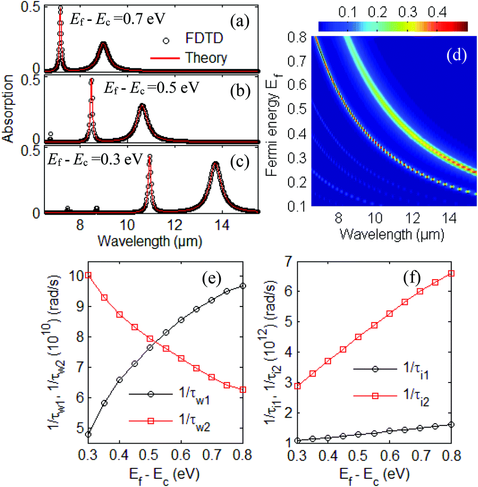 | ||
| Fig. 4 The absorption with different relative Fermi energies (a) Ef − Ec = 0.7 eV, (b) Ef − Ec = 0.5 eV, and (c) Ef − Ec = 0.3 eV using the CMT (red line) and FDTD method (black circles), respectively. (d) The evolution of linear-optical absorption for different relative Fermi energies with using the FDTD method. (e) 1/τw1 and 1/τw2 with various relative Fermi energies Ef − Ec. (f) 1/τi1 and 1/τi2 with various relative Fermi energies Ef − Ec. | ||
To get more insight into the BPSP structure, the parameters λm, 1/τwm, and 1/τim from CMT theory and FDTD simulation for different Ef − Ec are tabulated in Table 1. In the case of Ef − Ec = 0.3 eV in Fig. 4(c), the black phosphorus surface plasmon has two resonant wavelengths, λ1 = 10.9 μm and λ2 = 13.7 μm, obtained with the FDTD simulation. The parameter ωm (m = 1,2) in eqn (8) can be obtained with ωm = 2πc/λm. The absorption spectra A(ω) in eqn (8) can be obtained with appropriate parameters 1/τw1, 1/τw2, 1/τi1 and 1/τi2. We can precisely compare the intensity, resonant wavelength and spectral width of resonance absorption peaks A(ω) obtained by CMT with that of absorption spectrum simulated by the FDTD method in Fig. 4(c). We can then obtain the parameters in eqn (8) with 1/τw1 = 4.8 × 10¹⁰ rad s−1, 1/τw2 = 10 × 1010 rad s−1, 1/τi1 = 1.07 × 10¹² rad s−1, and 1/τi2 = 2.9 × 10¹² rad s−1. A similar process can be applied for other cases, Ef − Ec = 0.35 eV, 0.4 eV, 0.45 eV, 0.5 eV, 0.55 eV, 0.6 eV, 0.65 eV, 0.7 eV, 0.75 eV, and 0.8 eV, respectively. All the parameters λm, 1/τwm, and 1/τim (m = 1,2) can be obtained with different Ef − Ec in Table 1.
| Items | Parameters | |||||||||||
|---|---|---|---|---|---|---|---|---|---|---|---|---|
| Case | E f − Ec (eV) | 0.3 | 0.35 | 0.4 | 0.45 | 0.5 | 0.55 | 0.6 | 0.65 | 0.7 | 0.75 | 0.8 |
| FDTD | λ 1 (μm) | 10.9 | 10.1 | 9.50 | 8.90 | 8.50 | 8.10 | 7.70 | 7.40 | 7.20 | 6.90 | 6.70 |
| λ 2 (μm) | 13.7 | 12.7 | 11.9 | 11.2 | 10.6 | 10.1 | 9.70 | 9.30 | 9.00 | 8.70 | 8.40 | |
| Theory | 1/τw1 (1010) | 4.8 | 5.8 | 6.6 | 7.1 | 7.7 | 8.2 | 8.6 | 8.9 | 9.2 | 9.5 | 9.7 |
| 1/τw2 (1010) | 10.0 | 9.3 | 8.7 | 8.3 | 7.9 | 7.6 | 7.3 | 7.0 | 6.7 | 6.4 | 6.3 | |
| 1/τi1 (1012) | 1.07 | 1.12 | 1.17 | 1.22 | 1.29 | 1.32 | 1.41 | 1.43 | 1.50 | 1.55 | 1.62 | |
| 1/τi2 (1012) | 2.9 | 3.3 | 3.7 | 4.1 | 4.5 | 4.9 | 5.3 | 5.7 | 6.0 | 6.3 | 6.6 | |
The parameters 1/τwm and 1/τim (m = 1,2) with different Ef − Ec in Table 1 have fitting expressions as follows: 1/τw1 = −1.25 × 10¹⁰ + 24.85 × 10¹⁰(Ef − Ec) − 14.05 × 10¹⁰(Ef − Ec)2, 1/τw2 = 14.19 × 10¹⁰ − 16.79 × 10¹⁰(Ef − Ec) + 8.63 × 10¹⁰(Ef − Ec)2, 1/τi1 = 0.74 × 10¹² + 1.09 × 10¹²(Ef − Ec), 1/τi2 = 0.04 × 10¹² + 10.14 × 10¹²(Ef − Ec) − 2.38 × 10¹²(Ef − Ec)2. In the process of energy coupling between each mode and the light field, the decay rate for 1/τw1 and 1/τw2 with various relative Fermi energies Ef − Ec are shown in Fig. 4(e). In the process of intrinsic loss for the mth mode, the decay rate for 1/τi1 and 1/τi2 with various relative Fermi energies Ef − Ec are shown in Fig. 4(f). The lifetime τwm (m = 1,2) can be modulated with the relative Fermi energy Ef − Ec. As previously mentioned, adjusting the applied voltage or doping concentration corresponds to a change in the Fermi energy Ef. The lifetimes τwm (m = 1,2) strongly depend on the relative Fermi energy Ef − Ec, which can be electrostatically tuned, thus resulting in the sensing application with applied voltage bias.
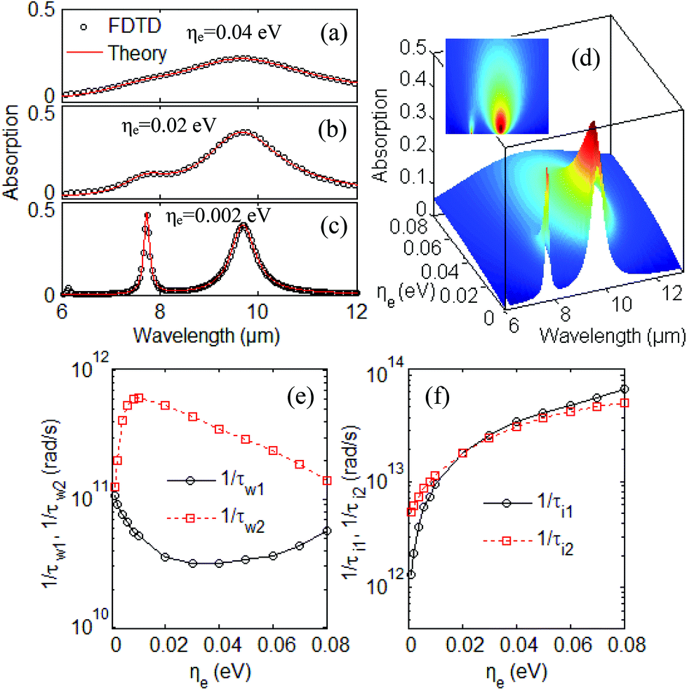
To get more insight into the loss in BPSP structure, the absorption spectra with different modulated parameters ηe (a) ηe = 0.04 eV, (b) ηe = 0.02 eV, and (c) ηe = 0.002 eV are depicted in Fig. 5 by using the CMT theory (red line) and the FDTD method (black circles), respectively. The simulated absorption spectra with the FDTD method show good agreement with the theoretical CMT results. The absorption spectra become broader and shallower when the scattering rate ηe increases from ηe = 0.002 eV to ηe = 0.04 eV. As the scattering rate ηe increases, the absorption for the resonant wavelength 7.7 μm drops from 48% to 14%, while the absorption for the resonant wavelength 9.7 μm drops from 46% to 24% as shown in Fig. 5(a)–(c). The change in the absorption amplitude and width of the spectra with FDTD simulation can also be well elaborated by CMT theory.
 | ||
| Fig. 5 The absorption with different scattering rates (a) ηe = 0.04 eV, (b) ηe = 0.02 eV, and (c) ηe = 0.002 eV by using the CMT theory (red line) and FDTD method (black circles), respectively. (d) The evolution of the linear-optical absorption for different ηe with the FDTD method. The inset in (d) is the top view. (e) 1/τw1 and 1/τw2 with various ηe. (f) 1/τi1 and 1/τi2 with various ηe. | ||
The evolution of the linear-optical absorption spectra for different ηe is shown in Fig. 5(d). With decreasing the scattering rate ηe, the absorption intensities of the two resonance modes decay exponentially. This exponential decay response characteristic is especially valuable for the application of conversion efficiency in the optoelectronic devices of black phosphorus.
The relative Fermi energy Ef − Ec = 0.6 eV is fixed here. Similar process in Table 1 can be applied for the cases ηe = 0.001 eV, 0.002 eV, 0.004 eV, 0.006 eV, 0.008 eV, 0.01 eV, 0.02 eV, 0.03 eV, 0.04 eV, 0.05 eV, 0.06 eV, 0.07 eV and 0.08 eV. The absorption spectra A(ω) can be obtained with appropriate parameters 1/τw1, 1/τw2, 1/τi1 and 1/τi2 for one case, ηe. We can then precisely compare the intensity, resonant wavelength and spectral width of the resonance absorption peaks A(ω) with that of the absorption spectrum simulated by the FDTD method. The parameters λm, 1/τwm, and 1/τim from CMT theory and FDTD simulation for the different scattering rate ηe are tabulated in Table 2.
| Items | Parameters | |||||||||||||
|---|---|---|---|---|---|---|---|---|---|---|---|---|---|---|
| Case | η e (eV) | 0.001 | 0.002 | 0.004 | 0.006 | 0.008 | 0.01 | 0.02 | 0.03 | 0.04 | 0.05 | 0.06 | 0.07 | 0.08 |
| FDTD | λ 1 (μm) | 7.7 | 7.7 | 7.7 | 7.7 | 7.7 | 7.7 | 7.7 | 7.7 | 7.7 | 7.7 | 7.7 | 7.7 | 7.7 |
| λ 2 (μm) | 9.7 | 9.7 | 9.7 | 9.7 | 9.7 | 9.7 | 9.7 | 9.7 | 9.7 | 9.7 | 9.7 | 9.7 | 9.7 | |
| Theory | 1/τw1 (1010) | 10.6 | 9.1 | 7.5 | 6.6 | 5.5 | 5.1 | 3.5 | 3.2 | 3.2 | 3.4 | 3.7 | 4.4 | 5.7 |
| 1/τw2 (1011) | 1.2 | 2.0 | 4.1 | 5.4 | 6.0 | 6.1 | 5.3 | 4.3 | 3.5 | 2.9 | 2.4 | 1.9 | 1.4 | |
| 1/τi1 (1012) | 1.3 | 2.1 | 3.7 | 5.7 | 7.1 | 9.3 | 18.3 | 26.9 | 36.7 | 43.7 | 51.7 | 62.0 | 73.9 | |
| 1/τi2 (1012) | 5.2 | 5.9 | 7.2 | 8.6 | 10.0 | 11.3 | 18.4 | 25.3 | 32.5 | 39.2 | 45.8 | 51.0 | 55.3 | |
The parameters 1/τwm and 1/τim (m = 1,2) with different ηe in Table 2 have the fitting expressions as follows: 1/τw1 = 3.1 × 10¹³ηe2 − 2.79 × 10¹²ηe + 8.78 × 10¹⁰, 1/τw2 = −7.14 × 10¹⁵ηe2 + 1.34 × 10¹⁴ηe − 1.88 × 10¹⁰ (if ηe < 0.01 eV), or 1/τw2 = 4.47 × 10¹³ηe2 − 1.07 × 10¹³ηe + 7.15 × 10¹¹ (if ηe > 0.01 eV), 1/τi1 = 8.92 × 10¹⁴ηe + 1.57 × 10¹¹, 1/τi2 = 6.59 × 10¹⁴ηe + 4.94 × 10¹². In the process of the energy coupling between each mode and the light field, the decay rate for 1/τw1 and 1/τw2 with various ηe are shown in Fig. 5(e). In the process of intrinsic loss for the mth mode, the decay rate for 1/τi1 and 1/τi2 with various ηe are plotted in Fig. 5(f). Therefore, the lifetimes τw1, τw2, τi1 and τi2 can be modulated with the scattering rate ηe.
There is a good broad tunability of the BPSP in black phosphorus by changing the side length L. To get more insight into the BPSP structure, the absorption spectra with different modulated side lengths (a) L = 160 nm, (b) L = 120 nm, and (c) L = 80 nm are shown in Fig. 6 using the CMT theory (red line) and FDTD method (black circles), respectively. The change in resonance wavelength, absorption amplitude, and width of the spectra can be well elaborated by CMT theory. The simulated absorption spectra with the FDTD method are in good agreement with the theoretical CMT results.
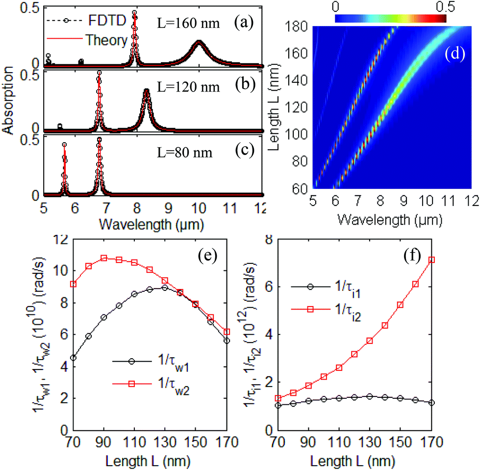 | ||
| Fig. 6 The absorption with different side lengths (a) L = 160 nm, (b) L = 120 nm, and (c) L = 80 nm using the CMT theory (red line) and FDTD method (black circles), respectively. (d) The evolution of linear-optical absorption for different side lengths L with the FDTD method. (e) 1/τw1 and 1/τw2 with various side lengths L. (f) 1/τi1 and 1/τi2 with various side lengths L. | ||
Additionally, the optical properties of the BP grating can be modulated by their side length. The evolution of the simulated linear-optical absorption spectra for different side lengths L was investigated with the FDTD method as shown in Fig. 6(d). The two resonance modes are red-shifted with increasing edge length L. This quasi-linear response characteristic in Fig. 6(d) between the edge length L and resonant wavelength is especially valuable for the application in the optoelectronic devices of black phosphorus.
The parameter Ef − Ec and the scattering rate ηe are fixed with 0.6 eV and 0.001 eV for various side lengths L, respectively. A similar process in Table 1 can be applied for the cases L = 70 nm, 80 nm, 90 nm, 100 nm, 110 nm, 120 nm, 130 nm, 140 nm, 150 nm, 160 nm, and 170 nm using CMT theory and FDTD simulation. The appropriate parameters 1/τw1, 1/τw2, 1/τi1 and 1/τi2 for one case with ηe can be obtained after precisely comparing resonance absorption peaks A(ω) with the absorption spectrum simulated by the FDTD method. We can then obtain the parameters λm, 1/τwm, and 1/τim (m = 1,2) for all the cases with side length L in Table 3.
| Items | Parameters | |||||||||||
|---|---|---|---|---|---|---|---|---|---|---|---|---|
| Case | L (nm) | 70 | 80 | 90 | 100 | 110 | 120 | 130 | 140 | 150 | 160 | 170 |
| FDTD | λ 1 (μm) | 5.5 | 5.7 | 6.1 | 6.2 | 6.6 | 6.7 | 7.2 | 7.3 | 7.7 | 7.9 | 8.4 |
| λ 2 (μm) | 6.7 | 6.8 | 7.4 | 7.6 | 8.2 | 8.3 | 8.9 | 9.1 | 9.7 | 10.0 | 10.8 | |
| Theory | 1/τw1 (1010) | 4.5 | 5.9 | 7.1 | 7.8 | 8.5 | 8.8 | 9.0 | 8.6 | 7.9 | 6.8 | 5.6 |
| 1/τw2 (1010) | 9.2 | 10.3 | 10.8 | 10.7 | 10.5 | 10.1 | 9.4 | 8.7 | 7.9 | 7.1 | 6.2 | |
| 1/τi1 (1012) | 1.02 | 1.12 | 1.22 | 1.29 | 1.35 | 1.38 | 1.40 | 1.38 | 1.33 | 1.25 | 1.13 | |
| 1/τi2 (1012) | 1.32 | 1.55 | 1.85 | 2.24 | 2.61 | 3.16 | 3.73 | 4.38 | 5.22 | 6.11 | 7.11 | |
The decay rates 1/τwm and 1/τim (m = 1,2) with different side lengths L in Table 3 have the fitting expressions as follows: 1/τw1 = −1.5 × 10⁷L2 + 3.7 × 10⁹L − 1.5 × 10¹¹, 1/τw2 = −9.3 × 10⁶L2 + 1.9 × 10⁹L + 1.2 × 10¹⁰, 1/τi1 = −1.2 × 10⁸L2 + 3.1 × 10¹⁰L − 5.6 × 10¹¹, 1/τi2 = 4.3 × 10⁸L2 − 4.7 × 10¹⁰L2 + 2.5 × 10¹². In the process of energy coupling between each mode and the light field, the decay rates for 1/τw1 and 1/τw2 with various side lengths L are shown in Fig. 6(e). In the process of intrinsic loss for the mth mode, the decay rates for 1/τi1 and 1/τi2 with various side lengths L are shown in Fig. 6(f). The lifetimes τw1, τw2, τi1 and τi2 can be changed with the modulated side length L. The expressions of the lifetimes for resonant modes in CMT are obtained from theoretical fitting of exact values in the FDTD simulation. The theoretical descriptions of the tunable lifetimes will be useful in applying the theory for future black phosphorus applications by changing the side length of BP.
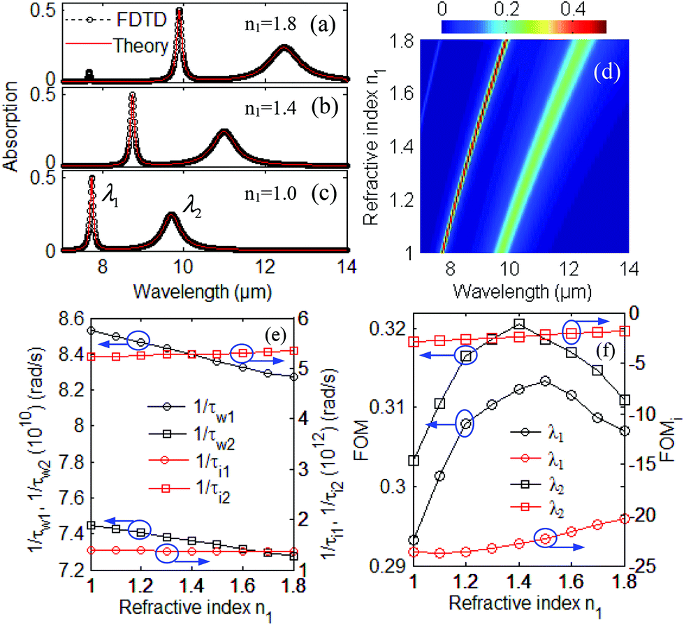
Since the intensities, wavelengths and spectral widths of resonance peaks can be precisely controlled with the Fermi energy Ef, the scattering rate ηe and side length L, we now discuss the sensing performance of the proposed nanosensor. Here, the parameters are those used in Fig. 2(a). In the following discussion, we only modify the refractive index n1 of superstrates such as an aqueous solution.
The absorption spectra with different refractive indexes of superstrates (a) n1 = 1.8, (b) n1 = 1.4, and (c) n1 = 1.0, are shown in Fig. 7 with the CMT (red line) and FDTD method (black circles), respectively. The change in resonance wavelength, absorption amplitude and broad of spectra with FDTD simulation can be well elaborated by CMT theory. Additionally, the evolution of the simulated linear-optical absorption spectra for different refractive indexes of superstrates, n1, was investigated with the FDTD method as shown in Fig. 7(d). The two resonance modes are red-shifted with increasing refractive index n1. This quasi-linear response characteristic in Fig. 7(d) between the refractive index n1 and the resonant wavelength is especially valuable for the sensing application of black phosphorus.
 | ||
| Fig. 7 The absorption with different refractive indexes n1 of superstrate (a) n1 = 1.8, (b) n1 = 1.4, and (c) n1 = 1.0 using the CMT theory (red line) and FDTD method (black circles), respectively. (d) The evolution of the linear-optical absorption for different refractive indexes n1 of the superstrate with the FDTD method. (e) 1/τw1, 1/τw2, 1/τi1 and 1/τi2 with various refractive indexes n1. (f) The sensitivity FOM and FOMi with various refractive indexes n1. | ||
Similar processes to that in Table 1 can be applied for the cases of the refractive indexes of superstrates, where n1 = 1.0, 1.1, 1.2, 1.3, 1.4, 1.5, 1.6, 1.7, and 1.8, using CMT theory and FDTD simulation. The appropriate parameters 1/τw1, 1/τw2, 1/τi1 and 1/τi2 for one case, n1, can be obtained after precisely comparing the intensity, resonant wavelength and spectral width of resonance absorption peaks A(ω) in eqn (8) with those of absorption spectra simulated by FDTD method. The parameters λm, 1/τwm, and 1/τim (m = 1,2) can then be obtained for all the cases of superstrate refractive indexes n1 in Table 4.
| Items | Parameters | |||||||||
|---|---|---|---|---|---|---|---|---|---|---|
| Case | n 1 | 1.0 | 1.1 | 1.2 | 1.3 | 1.4 | 1.5 | 1.6 | 1.7 | 1.8 |
| FDTD | λ 1 (μm) | 7.7 | 7.9 | 8.2 | 8.5 | 8.7 | 9.0 | 9.3 | 9.6 | 9.9 |
| λ 2 (μm) | 9.7 | 8.9 | 10.3 | 10.6 | 11.0 | 11.3 | 11.7 | 12.1 | 12.7 | |
| Theory | 1/τw1 (1010) | 8.48 | 8.54 | 8.49 | 8.35 | 8.34 | 8.32 | 8.31 | 8.29 | 8.22 |
| 1/τw2 (1010) | 7.45 | 7.40 | 7.39 | 7.35 | 7.31 | 7.29 | 7.25 | 7.28 | 7.27 | |
| 1/τi1 (1012) | 1.39 | 1.39 | 1.39 | 1.37 | 1.37 | 1.37 | 1.37 | 1.37 | 1.36 | |
| 1/τi2 (1012) | 5.24 | 5.23 | 5.26 | 5.26 | 5.26 | 5.28 | 5.28 | 5.33 | 5.34 | |
The parameters 1/τwm and 1/τim (m = 1,2) with different refractive indexes n1 of the superstrates in Table 4 have the fitting expressions as follows: 1/τw1 = −3.3 × 10⁹n1 + 8.9 × 10¹⁰, 1/τw2 = −2.2 × 10⁹n1 + 7.7 × 10¹⁰, 1/τi1 = −4 × 10¹⁰n1 + 1.4 × 10¹², 1/τi2 = 1.3 × 10¹¹n1 + 5.1 × 10¹². In the process of energy coupling between each mode and light field, the decay rate for 1/τw1 and 1/τw2 with various refractive indexes n1 are shown in Fig. 7(e). In the process of intrinsic loss for the mth mode, the decay rate for 1/τi1 and 1/τi2 with various n1 of the superstrates are shown in Fig. 7(e). The lifetimes τw1, τw2, τi1 and τi2 can be modulated with the modulated refractive index n1 of the superstrate. The expressions of the lifetimes for resonant modes in CMT were obtained from the theoretical fitting of the exact values in the FDTD simulation. The theoretical descriptions of the tunable lifetime will make it useful in applying the theory for future black phosphorus sensing applications by changing the refractive index n1 of superstrates such as aqueous solutions.
It is known that there are two common ways to describe the figure of merit (FOM) of a sensor.42 One is related to the resonance wavelengths shift at a certain refractive index n1, which is defined as FOM. The other is defined as FOMi, which is related to the intensity variation at a certain resonance wavelength λ. In order to quantitatively describe the sensitivity of the purposed sensor, we investigated the change in two resonance wavelengths by varying the refractive index n1 of the superstrate. We define the sensitivity as follows:
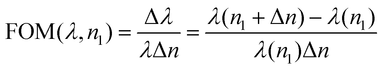 | (11) |
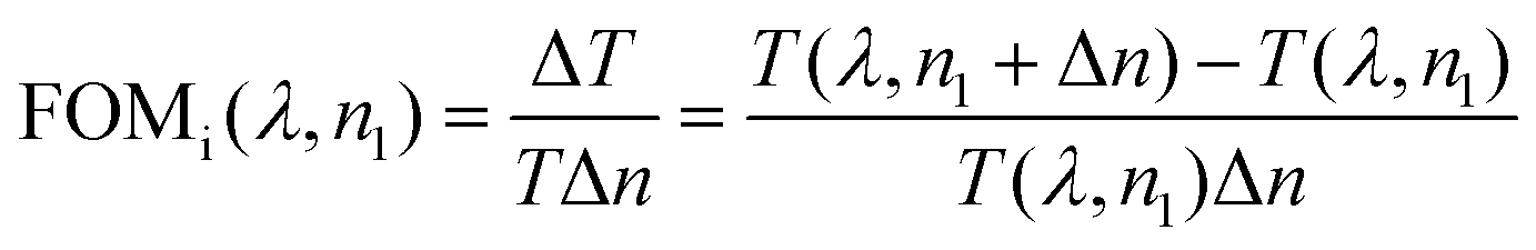 | (12) |
The sensing response FOM and FOMi can be obtained when the superstrate refractive index n1 increases from 1.0 to 1.8 as shown in Fig. 7(f). By using eqn (11), we get a FOM of 0.293 for resonance peak 1 at λ1 and 0.303 for resonance peak 2 at λ2 at refractive index n1 = 1. It can be seen that the FOM for peak 1 and peak 2 increase accordingly as the refractive index n1 increases from 1.0 to 1.4. However, FOM for peak 1 and peak 2 decrease as the refractive index n1 continues to increase from 1.4 to 1.8. By using eqn (12), we get a FOMi of −24 for peak 1 and −3.0 for peak 2 at refractive index n1 = 1. It can be seen that FOMi for peak 1 and peak 2 increase as the refractive index n1 increases from 1.0 to 1.8.
5. Conclusion
We have investigated the modulated surface plasmons and their modulated lifetimes for nanostructured black phosphorus. The expressions of the lifetimes for linear-optical resonant modes have been investigated with the FDTD simulations and CMT. The lifetimes of plasmonic absorption modes are tunable with the Fermi energy, collision frequency, side length and superstrate. The theoretical descriptions and data fitting are useful in applying the methods for future black phosphorus modulation. The strongly confined black phosphorus plasmonic waves result from an enhancement of the local field. The strongly localized field induces a desired increase in the second-order nonlinearity. It may stimulate new insights to visualize general nonlinear nanophotonic processes in black phosphorus. The proposed configuration and results could provide guidance for the research of the lifetimes of modes in black phosphorus, and the design of black phosphorus-based optoelectronic modulation devices and sensing applications.Data availability
The data that support the findings of this study are available from the corresponding authors upon request.Conflicts of interest
There are no conflicts to declare.Appendix
Optical conductivity model of multilayer black phosphorus
The electron effective masses mbp of black phosphorus along the x- and y-directions near the Γ point in the Hamiltonian model can be characterized as a diagonal tensor: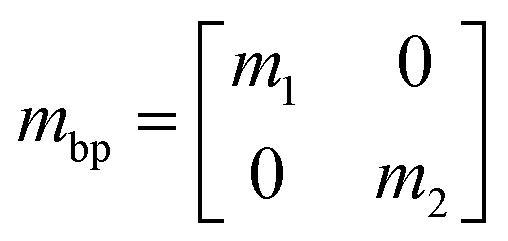 | (13) |
 | (14) |
 | (15) |
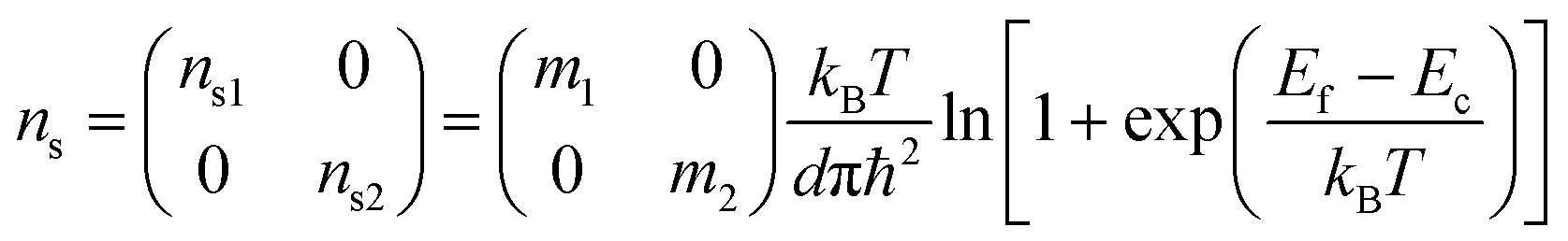
The electronic density ns of black phosphorus with thickness d is given by a diagonal tensor:43,12–15
 | (16) |
The incident electromagnetic wave can couple with the dipole and excite the corresponding plasmon oscillation in black phosphorus. The electric field inside the black phosphorus is a superposition of a wave decaying on the order of the skin depth and of the depolarization field. In the case of plasmons, which also comprise a magnetic dipole moment, the linear-optical coupling strength of the electric field to the plasmon is usually stronger than that of the magnetic field. The linear polarization P(1) = (−e) nsr(1) can be related to electrons with charge (−e) and density ns being displaced by r(1) from their equilibrium position. In linear optics, the linear polarization P(1) is simply proportional to the electric field:
 | (17) |
This allows us to define an equivalent relative permittivity diagonal tensor εD(ε11, ε22, ε33) to describe the black phosphorus with thickness d.
The conductivity of few-layer black phosphorus is given as
 | (18) |
 | (19) |
| ε33 = εr. | (20) |
Fundamental wave and second harmonic wave
Herein, the black phosphorus flake is treated as a thin layer with the anisotropic Drude model. The linear optical response of the black phosphorus in Maxwell equations is given by the following:24 | (21) |
 | (22) |
 | (23) |
 | (24) |
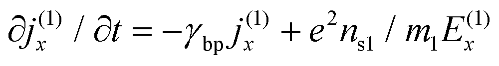
We can use the finite difference for eqn (24)
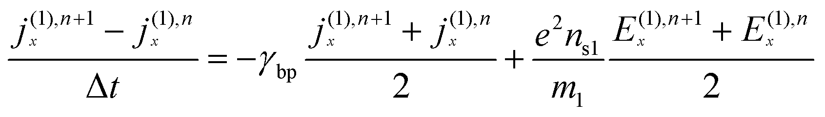
Eq. (24) can be simplified as follows:
| j(1),n+1x = k1j(1),nx + k2 (E(1),n+1x + E(1),nx) | (25) |
Similar to eqn (25), we can obtain the equation j(1),n+1y = k1j(1),ny + k3 (E(1),n+1y + E(1),ny) with using k3 = 0.5e2ns2Δt/m2/[1 + γbpΔt/2].
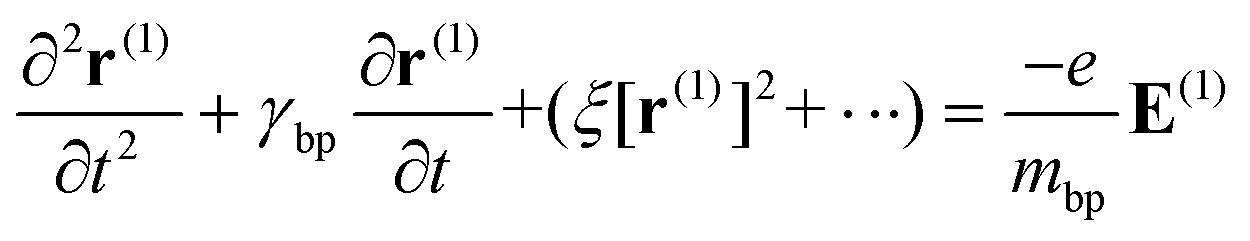
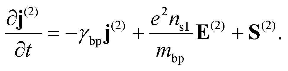
For the second order of the electric field, ξ ≠ 0 in eqn (14). ξ [r(1)]2 is the driving term for the second-order displacement r(2). The second-order polarization is P(2) ∝ r(2) and the second-order displacement is r(2) ∝ [r(1)]2. The second-order nonlinearity in nanostructured black phosphorus is described by the nonlinear Lorentz force acting on the black phosphorus electrons. The nonlinear theory has been formulated based on the Vlasov–Maxwell equations. The equations of second-order nonlinearity in black phosphorus grating can be described as follows:24
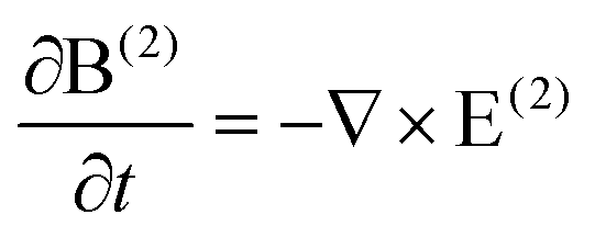 | (26) |
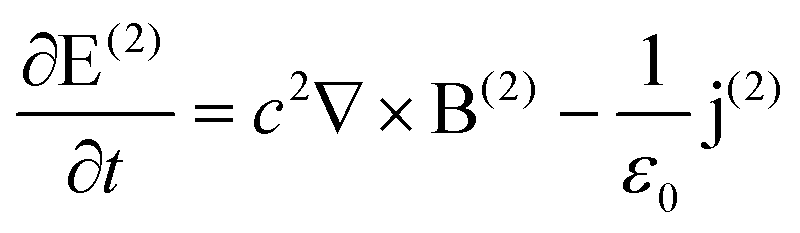 | (27) |
 | (28) |
Here The j(2), B(2), and E(2) represent the current density vector, magnetic flux intensity vector, and the electric field vector of SHW, which are marked with the superscript (2).
Numerical simulation
The 3D-FDTD method was used for the calculations. There are two computational loops for the calculations of the above first-order eqn (21)–(23), and the second-order eqn (26)–(28) in the program. Yee's discretization scheme was utilized and all electric and magnetic components in a cubic grid can be defined. The perfectly matched absorbing boundary conditions were used below and on top of the computational space along the z-direction, and the periodic boundary conditions were employed on the boundaries along the x- and y-directions. We only considered one unit cell in the computational space. The incident plane wave, polarized along the x-direction, propagates along the z-direction. The grid size of 2 nm was used to mesh the BP thin film, SiO2 substrate and the superstrate of an aqueous solution, respectively. The refractive index of the SiO2 was set as 1.4.Measurement nonlinear signals of FW and SHW
It is quite necessary to discuss the feasibility of the experimental demonstration. Similar to graphene and monolayer MoS2, the patterned black phosphorus can be fabricated using the standard procedure of nanofabrication. The processes are described as follows. First, 300 nm photoresist (i.e. ZEP520 or PMMA) is coated on the top of the black phosphor film. Then, the patterned photoresist was defined using electron beam lithography. Finally, the black phosphorus pattern was generated with reactive ion etching (i.e. O2 plasma or CHF3). The reflection and transmission of the structure for the fundamental wave can be measured by Fourier Transform Infrared Spectroscopy (FTIR). For the nonlinear response of the patterned black phosphorus, ultrafast laser pumps at two fundamental wavelengths were incident on the structure. The signal of nonlinear response was collected by the single mode fiber, which was integrated with the spectrometer.10,22,41,44 Measurements of SHG signals were also reported.25,31 Other measurements of third-order nonlinear signals were also reported.45,46Acknowledgements
The authors thank L. J. Huang of North Carolina State University for discussions of Measurement. This work was supported by the National Natural Science Foundation of China (11564014, 51675174, 61865006), Province Natural Science Foundation of Hunan (2016JJ6123, 2017JJ2097), and Scientific Research Fund of Hunan Provincial Education Department (15B191, 16A067) and Guangdong Provincial Education Department (2017KTSCX134).References
- L. Li, Y. Yu, G. J. Ye, Q. Ge, X. Ou, H. Wu, D. Feng, X. H. Chen and Y. Zhang, Black phosphorus field-effect transistors, Nat. Nanotechnol., 2014, 9(5), 372–377 CrossRef CAS PubMed.
- S. C. Dhanabalan, J. S. Ponraj, H. Zhang and Q. L. Bao, Present perspectives of broadband photodetectors based on nanobelts, nanoribbons, nanosheets and the emerging 2D materials, Nanoscale, 2016, 8, 6410–6434 RSC.
- J. Wang, H. Fang, X. Wang, X. Chen, W. Lu and W. Hu, Recent Progress on Localized Field Enhanced Two-dimensional Material Photodetectors from Ultraviolet-Visible to Infrared, Small, 2017, 13(35), 1700894–1700817 CrossRef PubMed.
- J. Miao, W. Hu, Y. Jing, W. Luo, L. Liao, A. Pan, S. Wu, J. Cheng, X. Chen and W. Lu, Surface Plasmon-Enhanced Photodetection in Few-Layer MoS2 Phototransistors with Au Nanostructure Arrays, Small, 2015, 11, 2392–2398 CrossRef CAS PubMed.
- Y. Chen, G. Jiang, S. Chen, Z. Guo, X. Yu, C. Zhao, H. Zhang, Q. Bao, S. Wen, D. Tang and D. Fan, Mechanically exfoliated black phosphorus as a new saturable absorber for both Q-switching and mode-locking laser operation, Opt. Express, 2015, 23(10), 12823–12833 CrossRef CAS PubMed.
- Z. C. Luo, M. Liu, Z. N. Guo, X. F. Jiang, A. P. Luo, C. J. Zhao, X. F. Yu, W. C. Xu and H. Zhang, Microfiber-based few-layer black phosphorus saturable absorber for ultra-fast fiber laser, Opt. Express, 2015, 23(15), 20030–20039 CrossRef CAS PubMed.
- J. Wang and Y. Jiang, Infrared absorber based on sandwiched two dimensional black phosphorus metamaterials, Opt. Express, 2017, 25(5), 5206–5216 CrossRef PubMed.
- S. B. Lu, L. L. Miao, Z. N. Guo, X. Qi, C. J. Zhao, H. Zhang, S. C. Wen, D. Y. Tang and D. Y. Fan, Broadband nonlinear optical response in multi-layer black phosphorus: an emerging infrared and mid-infrared optical material, Opt. Express, 2015, 23(9), 11183–11194 CrossRef CAS PubMed.
- P. M. Das, G. Danda, A. Cupo, W. Parkin, L. Liang, N. Kharche, X. Ling, S. Huang, M. S. Dresselhaus, V. Meunier and M. Drndic, Controlled Sculpture of Black Phosphorus Nanoribbons, ACS Nano, 2016, 10, 5687–5695 CrossRef PubMed.
- S. Lan, S. Rodrigues, L. Kang and W. Cai, Visualizing Optical Phase Anisotropy in Black Phosphorus, ACS Photonics, 2016, 3, 1176–1181 CrossRef CAS.
- S. C. Dhanabalan, J. S. Ponraj, Z. N. Guo, S. J. Li, Q. L. Bao and H. Zhang, Emerging Trends in Phosphorene Fabrication towardsNext Generation Devices, Adv. Sci., 2017, 4, 1600305 CrossRef PubMed.
- C. Lin, R. Grassi, T. Low and A. S. Helmy, Multilayer Black Phosphorus as a Versatile Mid-Infrared Electro-optic Material, Nano Lett., 2016, 16, 1683–1689 CrossRef CAS PubMed.
- X. Ni, L. Wang, J. Zhu, X. Chen and W. Lu, Surface plasmons in a nanostructured black phosphorus flake, Opt. Lett., 2017, 42(13), 2659–2662 CrossRef PubMed.
- Z. Liu and K. Aydin, Localized Surface Plasmons in Nanostructured Monolayer Black Phosphorus, Nano Lett., 2017, 16, 3457–3462 CrossRef PubMed.
- H. Lu, Y. Gong, D. Mao, X. Gan and J. Zhao, Strong plasmonic confinement and optical force in phosphorene pairs, Opt. Express, 2017, 25(5), 5255–5263 CrossRef CAS PubMed.
- J. S. Ponraj, Z. Xu, S. C. Dhanabalan, H. Mu, Y. Wang, J. Yuan, P. Li, S. Thakur, M. Ashrafi, K. Mccoubrey, Y. Zhang, S. Li, H. Zhang and Q. Bao, Photonics and optoelectronics of two dimensional materials beyond graphene, Nanotechnology, 2016, 27, 462001 CrossRef PubMed.
- L. Li, J. Kim, C. Jin, G. Ye, D. Y. Qiu, F. H. da Jornada, Z. Shi, L. Chen, Z. Zhang, F. Yang, K. Watanabe, T. Taniguchi, W. Ren, S. G. Louie, X. Chen, Y. Zhang and F. Wang, Direct observation of the layer-dependent electronic structure in phosphorene, Nat. Nanotechnol., 2016, 12, 21–25 CrossRef PubMed.
- C. Y. Xing, G. H. Jing, X. Liang, M. Qiu, Z. J. Li, R. Cao, X. J. Li, D. Y. Fan and H. Zhang, Graphene oxide/black phosphorus nanoflake aerogels with robust thermo-stability and significantly enhanced photothermal properties in air, Nanoscale, 2017, 9, 8096–8101 RSC.
- M. Pawliszewska, Y. Ge, Z. Li and H. Zhang, Fundamental and harmonic mode-locking at 2.1 μm with black phosphorus saturable absorber, Opt. Express, 2017, 25(15), 16916–16921 CrossRef CAS PubMed.
- X. Chen, Y. Wang, Y. J. Xiang, G. B. Jiang, L. L. Wang, Q. L. Bao, H. Zhang, Y. Liu, S. C. Wen and D. Y. Fan, A Broadband Optical Modulator Based on a Graphene Hybrid Plasmonic Waveguide, J. Lightwave Technol., 2016, 34(21), 4948–4953 Search PubMed.
- K. Wang, B. M. Szydłowska, G. Wang, X. Zhang, J. J. Wang, J. J. Magan, L. Zhang, J. N. Coleman, J. Wang and W. J. Blau, Ultrafast Nonlinear Excitation Dynamics of Black Phosphorus Nanosheets from Visible to Mid-Infrared, ACS Nano, 2016, 10, 6923–6932 CrossRef CAS PubMed.
- P. M. Das, G. Danda, A. Cupo, W. Parkin, L. Liang, N. Kharche, X. Ling, S. Huang, M. S. Dresselhaus, V. Meunier and M. Drndic, Controlled Sculpture of Black Phosphorus Nanoribbons, ACS Nano, 2016, 10, 5687–5695 CrossRef PubMed.
- N. Youngblood, R. Peng, A. Nemilentsau, T. Low and M. Li, Layer Tunable Third-Harmonic Generation in Multilayer Black Phosphorus, ACS Photonics, 2017, 4, 8–14 CrossRef CAS.
- Y. Zeng, W. Hoyer, J. Liu, S. Koch and J. Moloney, Classical theory for second-harmonic generation from metallic nanoparticles, Phys. Rev. B: Condens. Matter Mater. Phys., 2009, 79(23), 235109–235109 CrossRef.
- J. A. van Nieuwstadt, M. Sandtke, R. H. Harmsen, F. B. Segerink, J. C. Prangsma, S. Enoch and L. Kuipers, Strong modification of the nonlinear optical response of metallic subwavelength hole arrays, Phys. Rev. Lett., 2006, 97, 146102 CrossRef CAS PubMed.
- M. Lobet, M. Sarrazin, F. Cecchet and A. Vlad, Probing graphene χ(2) using a gold photon sieve, Nano Lett., 2016, 16(1), 48–54 CrossRef CAS PubMed.
- T. H. Xiao, L. Gan and Z. Y. Li, Graphene surface plasmon polaritons transport on curved substrates, Photonics Res., 2015, 3(6), 300–307 CrossRef CAS.
- Z. Shi, T. Xiao, H. Guo and Z. Li, All-Optical Modulation of a Graphene-Cladded Silicon Photonic Crystal Cavity, ACS Photonics, 2015, 1(11), 1513–1518 CrossRef.
- Y. Yang, Z. Shi, J. Li and Z. Y. Li, Optical forces exerted on a graphene-coated dielectric particle by a focused Gaussian beam, Photonics Res., 2016, 4(2), 65–69 CrossRef CAS.
- R. Zhou, S. Yang, D. Liu and G. Cao, The confined surface plasmon and second harmonic waves in graphene nanoribbon arrays, Opt. Express, 2017, 25(25), 31478–31491 CrossRef PubMed.
- B. Wang, R. wang, R. Liu, X. Lu, J. Zhao and Z. Y. Li, Origin of Shape Resonance in Second-Harmonic Generation from Metallic Nanohole Arrays, Sci. Rep., 2013, 3, 2358 CrossRef PubMed.
- W. Tang, L. Wang, X. Chen, C. Liu, A. Yu and W. Lu, Dynamic metamaterial based on the graphene split ring high-Q Fano-resonnator for sensing applications, Nanoscale, 2016, 8(33), 15196–15204 RSC.
- N. Guo, W. Hu, X. Chen, L. Wang and W. Lu, Enhanced plasmonic resonant excitation in a grating gated field-effect transistor with supplemental gates, Opt. Express, 2013, 21, 1606–1614 CrossRef CAS PubMed.
- J. Qin, D. Zhao, S. Luo, W. Wang, J. Lu, M. Qiu and Q. Li, Strongly enhanced molecular fluorescence with ultra-thin optical magnetic mirror metasurfaces, Opt. Lett., 2017, 42(21), 4478–4481 CrossRef PubMed.
- Z. Zhang, H. Jia, X. Zheng, R. Yang, Z. Wang, G. Ye, X. Chen, J. Shan and P. Feng, Black phosphorus nanoelectromechanical resonators vibrating at very high frequencies, Nanoscale, 2015, 7(3), 877–884 RSC.
- D. T. Debu, S. J. Bauman, D. French, H. O. H. Churchil and J. B. Herzog, Tuning Infrared Plasmon Resonance of Black Phosphorene Nanoribbon with a Dielectric Interface, Sci. Rep., 2018, 8, 3224 CrossRef PubMed.
- Y. Deng, G. Cao, H. Yang, G. Li, X. Chen and W. Lu, Tunable and high-sensitivity sensing based on Fano resonance with coupled plasmonic cavities, Sci. Rep., 2017, 7, 10639 CrossRef PubMed.
- S. Cho, H. Koh, H. Yoo and H. Jung, Tunable Chemical Sensing Performance of Black Phosphorus by Controlled Functionalization with Noble Metals, Chem. Mater., 2017, 29(17), 7197–7205 CrossRef CAS.
- A. N. Abbas, B. Liu, L. Chen, Y. Ma, S. Cong, N. Aroonyadet, M. Kopf, T. Nilges and C. Zhou, Black Phosphorus Gas Sensors, ACS Nano, 2015, 9(5), 5618–5624 CrossRef CAS PubMed.
- Z. Ni, L. Ma, S. Du, Y. Xu, M. Yuan, H. Fang, Z. Wang, M. Xu, D. Li, J. Yang, W. Hu, X. Pi and D. Yang, Plasmonic Silicon Quantum Dots Enabled High-Sensitivity Ultra-Broadband Photodetection of Graphene-Based Hybrid Phototransistors, ACS Nano, 2017, 11(10), 9854–9862 CrossRef CAS PubMed.
- B. Deng, V. Tran, Y. Xie, H. Jiang, C. Li, Q. Guo, X. Wang, He Tian, S. J. Koester, H. Wang, J. J. Cha, Q. Xia, L. Yang and F. Xia, Efficient electrical control of thin-film black phosphorus bandgap, Nat. Commun., 2016, 8, 14474 CrossRef PubMed.
- S. Zhan, Y. Peng, Z. He, B. Li, Z. Chen, H. Xu and H. Li, Tunable nanoplasmonic sensor based on the asymmetric degree of Fano resonance in MDM waveguide, Sci. Rep., 2016, 6, 22428 CrossRef CAS PubMed.
- T. Low, R. Roldán, H. Wang, F. Xia, P. Avouris, L. M. Moreno and F. Guinea, Plasmons and screening in monolayer and multilayer black phosphorus, Phys. Rev. Lett., 2014, 113(10), 106802–106805 CrossRef PubMed.
- C. Guo, Z. Zhu, X. Yuan, W. Ye, K. Liu, J. Zhang, W. Xu and S. Qin, Experimental Demonstration of Total Absorption over 99% in the Near Infrared for Monolayer-Graphene-Based Subwavelength Structures, Adv. Opt. Mater., 2016, 4(12), 1955–1960 CrossRef CAS.
- T. Jiang, D. Huang, J. Cheng, X. Fan, Z. Zhang, Y. Shan, Y. Yi, Y. Dai, L. Shi, K. Liu, C. Zeng, J. Zi, J. E. Sipe, Y. Shen, W. Liu and S. Wu, Gate-tunable third-order nonlinear optical response of massless Dirac Fermions in graphene, Nat. Photonics, 2018, 12, 430–436 CrossRef CAS.
- G. Soavi, G. Wang, H. Rostami, D. G. Purdie, D. D. Fazio, T. Ma, B. Luo, J. Wang, A. K. Ott, D. Yoon, S. A. Bourelle, J. E. Muench, I. Goykhman, S. D. Conte, M. Celebrano, A. Tomadin, M. Polini, G. Cerullo and A. C. Ferrari, Broadband, electrically tunable third-harmonic generation in graphene, Nat. Nanotechnol., 2018, 13, 583–588 CrossRef CAS PubMed.
- G. Cao, H. Li, S. Zhan, Z. He, Z. Guo, X. Xu and H. Yang, Uniform theoretical description of plasmon induced transparency in plasmonic stub waveguide, Opt. Lett., 2014, 39(2), 216–219 CrossRef PubMed.
- F. Gao, Z. Zhu, W. Xu, J. Zhang, C. Guo, K. Liu, X. Yuan and S. Qin, Broadband wave absorption in single-layered and nonstructured graphene based on farfield interaction effect, Opt. Express, 2017, 25, 9579–9586 CrossRef CAS PubMed.
| This journal is © The Royal Society of Chemistry 2018 |